 | –≠–ª–µ–∫—Ç—Ä–æ–Ω–Ω—ã–π –∫–æ–º–ø–æ–Ω–µ–Ω—Ç: ICX038DNA | –°–∫–∞—á–∞—Ç—å:  PDF PDF  ZIP ZIP |
Diagonal 8mm (Type 1/2) CCD Image Sensor for NTSC Color Video Cameras
Description
The ICX248AK is an interline CCD solid-state
image sensor suitable for NTSC color video cameras
with a diagonal 8mm (Type 1/2) system. Compared
with the current product ICX038DNA, basic
characteristics such as sensitivity, smear, dynamic
range and S/N are improved drastically through the
adoption of EXview HAD CCD
TM
technology.
This chip features a field period readout system and
an electronic shutter with variable charge-storage
time. This chip is compatible with the pins of the
ICX038DNA and has the same drive conditions.
EXview HAD CCD
TM
has different spectral characteristics
from the current CCD.
Features
∑ High sensitivity (+4.0dB compared with the ICX038DNA)
∑ Low smear (≠6dB compared with the ICX038DNA)
∑ High D range (+2.0dB compared with the ICX038DNA)
∑ High S/N
∑ High resolution and low dark current
∑ Excellent antiblooming characteristics
∑ Ye, Cy, Mg, and G complementary color mosaic filters on chip
∑ Continuous variable-speed shutter
∑ Substrate bias:
Adjustment free (external adjustment also possible with 6 to 14V)
∑ Reset gate pulse:
5Vp-p adjustment free (drive also possible with 0 to 9V)
∑ Horizontal register:
5V drive
Device Structure
∑ Interline CCD image sensor
∑ Image size:
Diagonal 8mm (Type 1/2)
∑ Number of effective pixels: 768 (H)
◊
494 (V) approx. 380K pixels
∑ Total number of pixels:
811 (H)
◊
508 (V) approx. 410K pixels
∑ Chip size:
7.95mm (H)
◊
6.45mm (V)
∑ Unit cell size:
8.4µm (H)
◊
9.8µm (V)
∑ Optical black:
Horizontal (H) direction : Front 3 pixels, rear 40 pixels
Vertical (V) direction
: Front 12 pixels, rear 2 pixels
∑ Number of dummy bits:
Horizontal 22
Vertical 1 (even fields only)
∑ Substrate material:
Silicon
≠ 1 ≠
E98614A99
Sony reserves the right to change products and specifications without prior notice. This information does not convey any license by
any implication or otherwise under any patents or other right. Application circuits shown, if any, are typical examples illustrating the
operation of the devices. Sony cannot assume responsibility for any problems arising out of the use of these circuits.
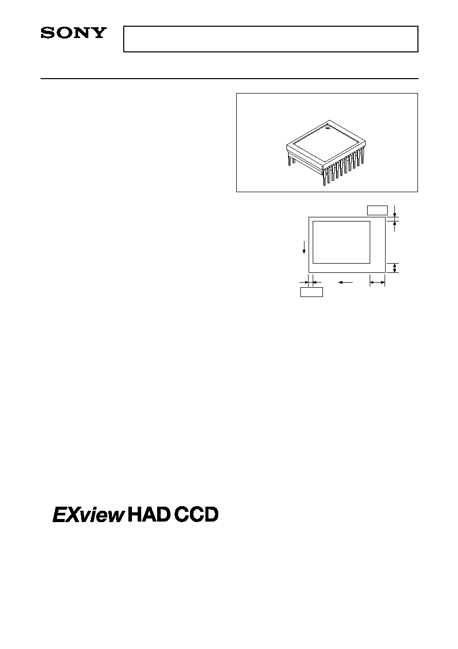
ICX248AK
20 pin DIP (Cer-DIP)
Pin 1
V
3
40
2
12
Pin 11
H
Optical black position
(Top View)
EXview HAD CCD is a trademark of Sony Corporation.
EXview HAD CCD is a CCD that drastically improves light efficiency by including near infrared light region as a basic structure of
HAD (Hole-Accumulation-Diode) sensor.
TM
≠ 2 ≠
ICX248AK
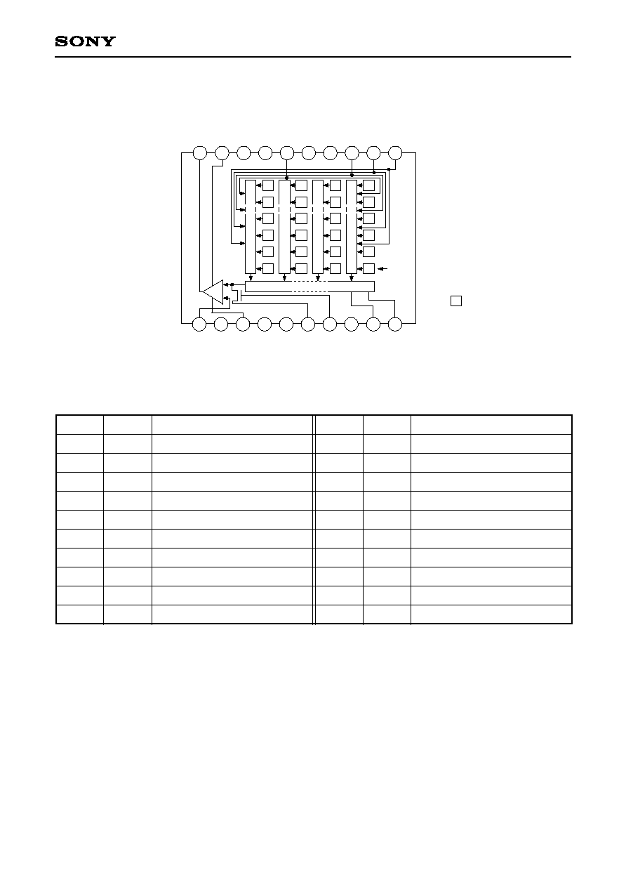
Pin No.
Symbol
Description
Pin No.
Symbol
Description
1
2
3
4
5
6
7
8
9
10
V
4
V
3
V
2
SUB
GND
V
1
V
L
GND
V
DD
V
OUT
Vertical register transfer clock
Vertical register transfer clock
Vertical register transfer clock
Substrate clock
GND
Vertical register transfer clock
Protective transistor bias
GND
Output circuit supply voltage
Signal output
11
12
13
14
15
16
17
18
19
20
V
GG
V
DSUB
V
SS
GND
GND
RD
RG
NC
H
1
H
2
Output circuit gate bias
Substrate bias circuit supply voltage
Output circuit source
GND
GND
Reset drain bias
Reset gate clock
Horizontal register transfer clock
Horizontal register transfer clock
1
2
3
4
5
6
7
8
9
10
11
12
13
14
15
16
Note)
Note) : Photo sensor
G
N
D
V
L
V
1
G
N
D
S
U
B
V
2
V
3
V
4
V
G
G
V
D
S
U
B
V
S
S
G
N
D
G
N
D
R
D
R
G
N
C
Horizontal Register
17
18
19
20
V
D
D
V
O
U
T
H
1
H
2
Cy
Mg
Cy
G
Cy
Mg
Ye
G
Ye
Mg
Ye
G
Cy
Mg
Cy
G
Cy
Mg
Ye
G
Ye
Mg
Ye
G
V
e
r
t
i
c
a
l
R
e
g
i
s
t
e
r
Block Diagram and Pin Configuration
(Top View)
Pin Description
≠ 3 ≠
ICX248AK
Item
≠0.3 to +50
≠0.3 to +18
≠55 to +10
≠15 to +20
to +10
to +15
to +17
≠17 to +17
≠10 to +15
≠55 to +10
≠65 to +0.3
≠0.3 to +30
≠30 to +80
≠10 to +60
V
V
V
V
V
V
V
V
V
V
V
V
∞C
∞C
1
Ratings
Unit
Remarks
Absolute Maximum Ratings
1
+27V (Max.) when clock width < 10µs, clock duty factor < 0.1%.
Substrate clock
SUB
≠ GND
V
DD
, V
RD
, V
DSUB
, V
OUT
, V
SS
≠ GND
Supply voltage
V
DD
, V
RD
, V
DSUB
, V
OUT
, V
SS
≠
SUB
V
1
, V
2
, V
3
, V
4
≠ GND
Clock input voltage
V
1
, V
2
, V
3
, V
4
≠
SUB
Voltage difference between vertical clock input pins
Voltage difference between horizontal clock input pins
H
1
, H
2
≠ V
4
RG
, V
GG
≠ GND
RG
, V
GG
≠
SUB
V
L
≠
SUB
Pins other than GND and
SUB
≠ V
L
Storage temperature
Operating temperature
≠ 4 ≠
ICX248AK
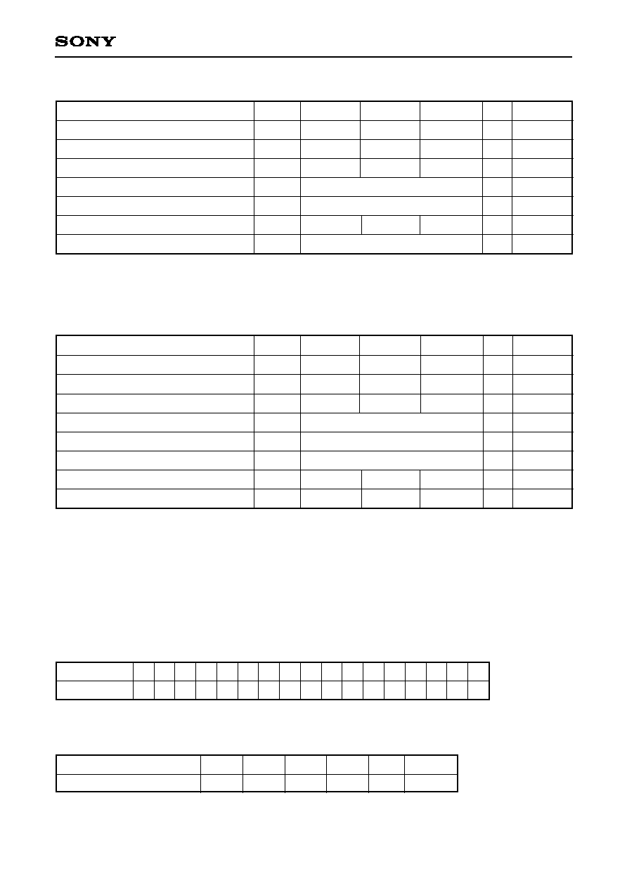
Item
V
DD
V
RD
V
GG
V
SS
V
L
V
DSUB
V
SUB
V
SUB
14.55
14.55
1.75
6.0
≠3
15.0
15.0
2.0
3
4
15.45
15.45
2.25
14.0
+3
V
V
V
V
%
V
RD
= V
DD
5
5
Symbol
Min.
Typ.
Max.
Unit
Remarks
Bias Conditions 2 [when used in substrate bias external adjustment mode]
Output circuit supply voltage
Reset drain voltage
Output circuit gate voltage
Output circuit source
Protective transistor bias
Substrate bias circuit supply voltage
Substrate voltage adjustment range
Substrate voltage adjustment precision
3
V
L
setting is the V
VL
voltage of the vertical transfer clock waveform, or the same supply voltage as the V
L
power supply for the V driver should be used. (When CXD1267AN is used.)
4
Connect to GND or leave open.
5
The setting value of the substrate voltage (V
SUB
) is indicated on the back of the image sensor by a special
code. When adjusting the substrate voltage externally, adjust the substrate voltage to the indicated voltage.
The adjustment precision is ±3%. However, this setting value has not significance when used in substrate
bias internal generation mode.
V
SUB
code -- one character indication
Code and optimal setting correspond to each other as follows.
DC Characteristics
Item
Output circuit supply current
I
DD
5.0
10.0
mA
Symbol
Min.
Typ.
Max.
Unit
Remarks
V
SUB
code
Optimal setting 6.0 6.5 7.0 7.5 8.0 8.5 9.0 9.5 10.0 10.5 11.0 11.5 12.0 12.5 13.0 13.5 14.0
E
f
G
h
J
K
L
m
N
P
Q
R
S
T
U
V
W
<Example> "L"
V
SUB
= 9.0V
Item
V
DD
V
RD
V
GG
V
SS
V
L
V
DSUB
SUB
14.55
14.55
1.75
14.55
15.0
15.0
2.0
1
15.0
2
15.45
15.45
2.25
15.45
V
V
V
V
V
RD
= V
DD
Symbol
Min.
Typ.
Max.
Unit
Remarks
Bias Conditions 1 [when used in substrate bias internal generation mode]
Output circuit supply voltage
Reset drain voltage
Output circuit gate voltage
Output circuit source
Protective transistor bias
Substrate bias circuit supply voltage
Substrate clock
Grounded with 390
resistor
1
V
L
setting is the V
VL
voltage of the vertical transfer clock waveform, or the same supply voltage as the V
L
power supply for the V driver should be used. (When CXD1267AN is used.)
2
Do not apply a DC bias to the substrate clock pin, because a DC bias is generated within the CCD.
Grounded with 390
resistor
≠ 5 ≠
ICX248AK
Item
Readout clock voltage
V
VT
V
VH1
, V
VH2
V
VH3
, V
VH4
V
VL1
, V
VL2
,
V
VL3
, V
VL4
V
V
| V
VH1
≠ V
VH2
|
V
VH3
≠ V
VH
V
VH4
≠ V
VH
V
VHH
V
VHL
V
VLH
V
VLL
V
H
V
HL
V
RGL
V
RG
V
RGLH
≠ V
RGLL
V
SUB
14.55
≠0.05
≠0.2
≠9.6
8.3
≠0.25
≠0.25
4.75
≠0.05
4.5
23.0
15.0
0
0
≠9.0
9.0
5.0
0
1
5.0
24.0
15.45
0.05
0.05
≠8.5
9.65
0.1
0.1
0.1
0.5
0.5
0.5
0.5
5.25
0.05
5.5
0.8
25.0
V
V
V
V
Vp-p
V
V
V
V
V
V
V
Vp-p
V
V
Vp-p
V
V
1
2
2
2
2
2
2
2
2
2
2
2
3
3
4
4
4
5
V
VH
= (V
VH1
+ V
VH2
)/2
V
VL
= (V
VL3
+ V
VL4
)/2
V
V
= V
VH
n ≠ V
VL
n (n = 1 to 4)
High-level coupling
High-level coupling
Low-level coupling
Low-level coupling
Low-level coupling
Horizontal transfer
clock voltage
Reset gate clock
voltage
1
Substrate clock voltage
Vertical transfer clock
voltage
Symbol
Min.
Typ. Max. Unit
Waveform
diagram
Remarks
Item
Symbol
Min.
Typ. Max. Unit
Waveform
diagram
Remarks
1
Input the reset gate clock without applying a DC bias. In addition, the reset gate clock can also be driven
with the following specifications.
Reset gate clock
voltage
V
RGL
V
RG
≠0.2
8.5
0
9.0
0.2
9.5
V
Vp-p
4
4
Clock Voltage Conditions