 | –≠–ª–µ–∫—Ç—Ä–æ–Ω–Ω—ã–π –∫–æ–º–ø–æ–Ω–µ–Ω—Ç: ICX267AK | –°–∫–∞—á–∞—Ç—å:  PDF PDF  ZIP ZIP |

≠ 1 ≠
E99947A33
Sony reserves the right to change products and specifications without prior notice. This information does not convey any license by
any implication or otherwise under any patents or other right. Application circuits shown, if any, are typical examples illustrating the
operation of the devices. Sony cannot assume responsibility for any problems arising out of the use of these circuits.
ICX267AK
20 pin DIP (Plastic)
Description
The ICX267AK is a diagonal 8mm (Type 1/2) interline
CCD solid-state image sensor with a square pixel array
and 1.45M effective pixels. Progressive scan allows all
pixels' signals to be output independently. Also, the
adoption of high frame rate readout mode supports
30 frames per second. This chip features an electronic
shutter with variable charge-storage time which
makes it possible to realize full-frame still image
without a mechanical shutter. High resolution and
high color reproductivity are achieved through the use
of R, G, B primary color mosaic filters. Further, high
sensitivity and low dark current are achieved through
the adoption of HAD (Hole-Accumulation Diode)
sensors.
This chip is suitable for applications such as
electronic still cameras, PC input cameras, etc.
Features
∑ Progressive scan allows individual readout of the
image signals from all pixels.
∑ High horizontal and vertical resolution (both approx.
800TV-lines) still image without a mechanical shutter.
∑ Supports high frame rate readout mode
(effective 512 lines output, 30 frames/s)
∑ Square pixel
∑ Horizontal drive frequency: 28.636MHz
∑ No voltage adjustments
(reset gate and substrate bias are not adjusted.)
∑ R, G, B primary color mosaic filters on chip
∑ High resolution, high color reproductivity,
high sensitivity, low dark current
∑ Low smear, excellent antiblooming characteristics
∑ Continuous variable-speed shutter
Device Structure
∑ Interline CCD image sensor
∑ Image size:
Diagonal 8mm (Type 1/2)
∑ Total number of pixels:
1434 (H)
◊
1050 (V) approx. 1.50M pixels
∑ Number of effective pixels: 1392 (H)
◊
1040 (V) approx. 1.45M pixels
∑ Number of active pixels:
1360 (H)
◊
1024 (V) approx. 1.40M pixels (7.959mm diagonal)
∑ Chip size:
7.60mm (H)
◊
6.20mm (V)
∑ Unit cell size:
4.65µm (H)
◊
4.65µm (V)
∑ Optical black:
Horizontal (H) direction: Front 2 pixels, rear 40 pixels
Vertical (V) direction:
Front 8 pixels, rear 2 pixels
∑ Number of dummy bits:
Horizontal 20
Vertical 3
∑ Substrate material:
Silicon
Diagonal 8mm (Type 1/2) Progressive Scan CCD Image Sensor with Square Pixel for Color Cameras
2
40
H
V
2
8
Pin 1
Pin 11
Optical black position
(Top view)
Wfine CCD is a registered trademark of Sony Corporation.
Represents a CCD adopting progressive scan, primary color filter and square pixel.
≠ 2 ≠
ICX267AK
Block Diagram and Pin Configuration
(Top View)
Pin No.
Pin No.
1
2
3
4
5
6
7
8
9
10
11
12
13
14
15
16
17
18
19
20
Pin Description
Note)
: Photo sensor
...
...
...
...
Note)
V
OUT
GND
NC
GND
NC
NC
V
3
V
2B
V
2A
V
1
V
DD
GND
SUB
NC
C
SUB
NC
V
L
RG
H
1
H
2
Vertical re
gister
Horizontal register
11
12
13
14
15
16
17
18
19
20
10
9
8
7
6
5
4
3
2
1
1
DC bias is generated within the CCD, so that this pin should be grounded externally through a capacitance
of 0.1µF.
Symbol
V
DD
GND
SUB
NC
C
SUB
NC
V
L
RG
H
1
H
2
Symbol
V
1
V
2A
V
2B
V
3
NC
NC
GND
NC
GND
V
OUT
Description
Supply voltage
GND
Substrate clock
Substrate bias
1
Protective transistor bias
Reset gate clock
Horizontal register transfer clock
Horizontal register transfer clock
Description
Vertical register transfer clock
Vertical register transfer clock
Vertical register transfer clock
Vertical register transfer clock
GND
GND
Signal output
≠ 3 ≠
ICX267AK
Absolute Maximum Ratings
1
+24V (Max.) when clock width < 10µs, clock duty factor < 0.1%.
+16V (Max.) is guaranteed for turning on or off power supply.
Item
V
DD
, V
OUT
,
RG ≠
SUB
V
2A
, V
2B
≠
SUB
V
1
, V
3
, V
L
≠
SUB
H
1
, H
2
, GND ≠
SUB
C
SUB
≠
SUB
V
DD
, V
OUT
,
RG, C
SUB
≠ GND
V
1
, V
2A
, V
2B
, V
3
≠ GND
H
1
, H
2
≠ GND
V
2A
, V
2B
≠ V
L
V
1
, V
3
, H
1
, H
2
, GND ≠ V
L
Voltage difference between vertical clock input pins
H
1
≠ H
2
H
1
, H
2
≠ V
3
Against
SUB
Against GND
Against V
L
Between input
clock pins
Storage temperature
Operating temperature
≠40 to +10
≠50 to +15
≠50 to +0.3
≠40 to +0.3
≠25 to
≠0.3 to +18
≠10 to +18
≠10 to +15
≠0.3 to +28
≠0.3 to +15
to +15
≠16 to +16
≠16 to +16
≠30 to +80
≠10 to +60
V
V
V
V
V
V
V
V
V
V
V
V
V
∞C
∞C
1
Ratings
Unit
Remarks
≠ 4 ≠
ICX267AK
Clock Voltage Conditions
Readout clock voltage
Vertical transfer clock
voltage
Horizontal transfer
clock voltage
Reset gate clock
voltage
Substrate clock voltage
V
VT
V
VH02A
V
VH1
, V
VH2A
,
V
VH2B
, V
VH3
V
VL1
, V
VL2A
,
V
VL2B
, V
VL3
V
1
, V
2A
,
V
2B
, V
3
| V
VL1
≠ V
VL3
|
V
VHH
V
VHL
V
VLH
V
VLL
V
H
V
HL
V
RG
V
RGLH
≠ V
RGLL
V
RGL
≠ V
RGLm
V
SUB
14.55
≠0.05
≠0.2
≠8.4
7.6
4.75
≠0.05
3.0
22.15
15.0
0
0
≠8.0
8.0
5.0
0
3.3
23.0
15.45
0.05
0.05
≠7.6
8.4
0.1
0.9
1.3
1.0
0.9
5.25
0.05
5.5
0.4
0.5
23.85
1
2
2
2
2
2
2
2
2
2
3
3
4
4
4
5
V
VH
= V
VH02A
V
VL
= (V
VL1
+ V
VL3
)/2
High-level coupling
High-level coupling
Low-level coupling
Low-level coupling
Low-level coupling
Low-level coupling
V
V
V
V
V
V
V
V
V
V
V
V
V
V
V
V
Bias Conditions
Power Supply voltage
Protective transistor bias
Substrate clock
Reset gate clock
Item
V
DD
V
L
SUB
RG
Symbol
15.0
1
2
2
Min.
V
Unit
Remarks
Typ.
Max.
1
V
L
setting is the V
VL
voltage of the vertical transfer clock waveform, or the same power supply as the V
L
power supply for the V driver should be used.
2
Do not apply a DC bias to the substrate clock and reset gate clock pins, because a DC bias is generated
within the CCD.
DC Characteristics
14.55
15.45
Power supply current
Item
I
DD
Symbol
7.7
Min.
Unit
Remarks
Typ.
Max.
mA
Item
Symbol
Min.
Typ.
Max.
Unit
Waveform
diagram
Remarks
≠ 5 ≠
ICX267AK
Clock Equivalent Circuit Constant
C
V1
C
V2A
C
V2B
C
V3
C
V12A
, C
V2B1
C
V2A3
, C
V32B
C
V13
C
H1
, C
H2
C
HH
C
RG
C
SUB
R
1
R
2A
, R
3
R
2B
R
GND
R
H
R
RG
Symbol
Capacitance between vertical transfer clock and
GND
Capacitance between vertical transfer clocks
Capacitance between horizontal transfer clock
and GND
Capacitance between horizontal transfer clocks
Capacitance between reset gate clock and GND
Capacitance between substrate clock and GND
Vertical transfer clock series resistor
Vertical transfer clock ground resistor
Horizontal transfer clock series resistor
Reset gate clock series resistor
Item
Min.
2200
3300
3300
3300
1200
1200
2200
47
100
8
680
36
56
56
30
15
20
Typ.
Max.
pF
pF
pF
pF
pF
pF
pF
pF
pF
pF
pF
Unit Remarks
Horizontal transfer clock equivalent circuit
Vertical transfer clock equivalent circuit
V
1
C
V12A
V
2A
V
2B
V
3
C
V32B
C
V2A3
C
V2B1
C
V13
C
V1
C
V2A
C
V2B
C
V3
R
GND
R
2B
R
1
R
3
R
2A
H
1
H
2
C
H1
C
H2
C
HH
R
H
R
H
Reset gate clock equivalent circuit
R
RG
RG
C
RG

≠ 6 ≠
ICX267AK
Drive Clock Waveform Conditions
(1) Readout clock waveform
(2) Vertical transfer clock waveform
V
VH
= V
VH02A
V
VL
= (V
VL01
+ V
VL03
)/2
V
VL3
= V
VL03
V
1
V
3
V
2A
, V
2B
100%
90%
10%
0%
tr
tf
0V
twh
M
2
M
V
VT
V
VH1
V
VHH
V
VH
V
VHL
V
VLH
V
VL1
V
VL01
V
VL
V
VLL
V
VH3
V
VHH
V
VH
V
VHL
V
VLH
V
VL03
V
VL
V
VLL
V
VLH
V
VL2A
, V
VL2B
V
VLL
V
VL
V
VH
V
VHH
V
VH02A
, V
VH02B
V
VH2A
, V
VH2B
V
VHL
V
V1
= V
VH1
≠ V
VL01
V
V2A
= V
VH02A
≠ V
VL2A
V
V2B
= V
VH02B
≠ V
VL2B
V
V3
= V
VH3
≠ V
VL03
V
T
Note) Readout clock is used by composing vertical transfer clocks V
2A
and V
2B
.
≠ 7 ≠
ICX267AK
(3) Horizontal transfer clock waveform
Cross-point voltage for the H
1
rising side of the horizontal transfer clocks H
1
and H
2
waveforms is V
CR
.
The overlap period for twh and twl of horizontal transfer clocks H
1
and H
2
is two.
(4) Reset gate clock waveform
V
RGLH
is the maximum value and V
RGLL
is the minimum value of the coupling waveform during the period from
Point A in the above diagram until the rising edge of RG.
In addition, V
RGL
is the average value of V
RGLH
and V
RGLL
.
V
RGL
= (V
RGLH
+ V
RGLL
)/2
Assuming V
RGH
is the minimum value during the interval twh, then:
V
RG
= V
RGH
≠ V
RGL
.
Negative overshoot level during the falling edge of RG is V
RGLm
.
(5) Substrate clock waveform
H
1
H
2
10%
90%
twh
tf
tr
twl
V
HL
V
H
two
V
CR
V
H
2
RG waveform
V
RGLH
V
RGH
V
RGL
V
RGLL
V
RGLm
tr
twh
twl
tf
V
RG
Point A
100%
90%
10%
0%
V
SUB
(A bias generated within the CCD)
tr
tf
twh
M
2
M
V
SUB
≠ 8 ≠
ICX267AK
Clock Switching Characteristics
Min.
twh
Typ. Max. Min. Typ. Max. Min. Typ. Max. Min. Typ. Max.
twl
tr
tf
3.2
10
10
4
3.4
12.5
12.5
8
3.9
10
10
12.5
12.5
24
0.5
5
5
0.01
0.01
2
7.5
7.5
0.5
15
2
0.5
5
5
0.01
0.01
450
7.5
7.5
0.5
Unit
µs
ns
ns
µs
ns
µs
Remarks
During
readout
1
2
During drain
charge
Item
Readout clock
Vertical transfer
clock
During
imaging
During
parallel-serial
conversion
Reset gate clock
Substrate clock
Hor
iz
ontal
transf
er cloc
k
1
When vertical transfer clock driver CXD1267AN
◊
2 is used.
2
tf
tr ≠ 2ns, and the cross-point voltage (V
CR
) for the H
1
rising side of the H
1
and H
2
waveforms must
be at least V
H
/2 [V].
Spectral Sensitivity Characteristics (excludes lens characteristics and light source characteristics)
1.0
0.8
0.6
0.4
0.2
0
400
500
600
700
Wave Length [nm]
Relativ
e Response
800
900
1000
Symbol
V
T
V
1
, V
2A
,
V
2B
, V
3
H
1
H
2
H
1
H
2
RG
SUB
Min.
two
Typ.
Max.
8
10
Unit
ns
Remarks
Item
Horizontal transfer clock
Symbol
H
1
, H
2

≠ 9 ≠
ICX267AK
Image Sensor Characteristics
(Ta = 25∞C)
G sensitivity
Sensitivity
comparison
Saturation signal
Smear
Video signal shading
Uniformity between
video signal channels
Dark signal
Dark signal shading
Line crawl G
Line crawl R
Line crawl B
Lag
Sg
Rr
Rb
Vsat
Vsat2
Vsat4
Sm
SHg
Srg
Sbg
Ydt
Ydt
Lcg
Lcr
Lcb
Lag
320
0.4
0.3
450
380
380
400
0.55
0.45
0.001
0.002
0.7
0.6
0.0025
0.005
20
25
8
8
8
2
3.8
3.8
3.8
0.5
mV
mV
mV
mV
%
%
%
%
%
%
mV
mV
%
%
%
%
1
1
1
2
2
2
3
3
4
4
5
5
6
7
8
8
8
9
1/30s accumulation
Progressive scan readout,
high frame rate readout two
pixels addition
High frame rate readout mode
Zone 0 and
I
Zone 0 to
I
I
'
Ta = 60∞C, 15 frames/s
Ta = 60∞C, 15 frames/s
2
Item
Symbol
Min.
Typ.
Max.
Unit
Measurement
method
Remarks
R
B
Progressive scan
readout mode
High frame rate
readout mode
High frame rate
readout two pixels
addition
1
1
Vsat4 is the saturation signal amount at two pixels addition, and it is 190mV per one pixel. V
SUB
internal
generation value ensures 190mV per one pixel of the saturation signal amount in high frame rate two pixels
addition mode.
2
Eliminates the dark signal shading in the vertical direction by the high-speed transfer of the vertical
register.
Ta = 60∞C
≠ 10 ≠
ICX267AK
Zone Definition of Video Signal Shading
16
V
10
16
8
8
Ignored region
Effective pixel region
Zone 0,
I
Zone
II
,
II
'
V
10
H
8
H
8
1392 (H)
1040 (V)
Measurement System
Note) Adjust the amplifier gain so that the gain between [
A] and [
B], and between [
A] and [
C] equals 1.
CCD
C.D.S
AMP
CCD signal output [
A]
Gr/Gb channel signal output [
B]
Gr/Gb
S/H
S/H
R/B channel signal output [
C]
R/B
Image Sensor Characteristics Measurement Method
Color coding and readout of this image sensor
The primary color filters of this image sensor are arranged in the layout
shown in the figure on the left (Bayer arrangement).
Gr and Gb denote the G signals on the same line as the R signal and
the B signal, respectively.
Gb
B
Gb
B
R
Gr
R
Gr
Gb
B
Gb
B
R
Gr
R
Gr
Horizontal register
Color Coding Diagram
All pixel signals are output successively in a 1/15s period.
The R signal and Gr signal lines and the Gb signal and B signal lines are output successively.
≠ 11 ≠
ICX267AK
Readout modes
The diagram below shows the output methods for the following three readout modes.
9 (V2A)
8 (V2B)
7 (V2B)
6 (V2A)
5 (V2A)
4 (V2B)
3 (V2B)
2 (V2A)
1 (V2A)
V
OUT
9 (V2A)
8 (V2B)
7 (V2B)
6 (V2A)
5 (V2A)
4 (V2B)
3 (V2B)
2 (V2A)
1 (V2A)
V
OUT
9 (V2A)
8 (V2B)
7 (V2B)
6 (V2A)
5 (V2A)
4 (V2B)
3 (V2B)
2 (V2A)
1 (V2A)
V
OUT
Progressive scan mode
High frame rate readout mode
High frame rate readout two pixels
addition mode
1. Progressive scan mode
In this mode, all pixels signals are output in non-interlace format in 1/15s.
The vertical resolution is approximately 800 TV-lines and all pixels signals within the same exposure period
are read out simultaneously, making this mode suitable for high resolution image capturing.
2. High frame rate readout mode
All effective areas are scanned in approximately 1/30s by reading out two out of four lines (3rd and 4th
lines, 7th and 8th lines). The vertical resolution is approximately 400 TV-lines.
This readout mode emphasizes processing speed over vertical resolution.
3. High frame rate readout two pixels addition mode
All effective areas are scanned in approximately 1/30s by reading out two out of four lines (3rd and 4th
lines, 7th and 8th lines), and by reading out two out of the remaining four lines (1st and 2nd lines, 5th and
6th lines) after shifting the vertical register by 2 bits, and adding them in the vertical register.

≠ 12 ≠
ICX267AK
Measurement conditions
1) In the following measurements, the device drive conditions are at the typical values of the progressive scan
mode, bias and clock voltage conditions.
2) In the following measurements, spot blemishes are excluded and, unless otherwise specified, the optical
black level (OB) is used as the reference for the signal output, which is taken as the value of the Gr/Gb
signal output or the R/B signal output of the measurement system.
Definition of standard imaging conditions
1) Standard imaging condition
I
:
Use a pattern box (luminance: 706cd/m
2
, color temperature of 3200K halogen source) as a subject.
(Pattern for evaluation is not applicable.) Use a testing standard lens with CM500S (t = 1.0mm) as an IR cut
filter and image at F5.6. The luminous intensity to the sensor receiving surface at this point is defined as the
standard sensitivity testing luminous intensity.
2) Standard imaging condition
I
I
:
Image a light source (color temperature of 3200K) with a uniformity of brightness within 2% at all angles.
Use a testing standard lens with CM500S (t = 1.0mm) as an IR cut filter. The luminous intensity is adjusted
to the value indicated in each testing item by the lens diaphragm.
1. G sensitivity, sensitivity comparison
Set to standard imaging condition
I
. After selecting the electronic shutter mode with a shutter speed of 1/100s,
measure the signal outputs (V
Gr
, V
Gb
, V
R
and V
B
) at the center of each Gr, Gb, R and B channel screen, and
substitute the values into the following formulas.
V
G
= (V
Gr
+ V
Gb
)/2
Sg = VG
◊
[mV]
Rr = V
R
/V
G
Rb = V
B
/V
G
2. Saturation signal
Set to standard imaging condition
I
I
. After adjusting the luminous intensity to 20 times the intensity with the
average value of the Gr signal output, 150mV, measure the minimum values of the Gr, Gb, R and B signal
outputs.
3. Smear
Set to standard imaging condition
I
I
. With the lens diaphragm at F5.6 to F8, first adjust the average value of
the Gr signal output to 150mV. Measure the average values of the Gr signal output, Gb signal output, R
signal output and B signal output (Gra, Gba, Ra, Ba), and then adjust the luminous intensity to 500 times
the intensity with the average value of the Gr signal output, 150mV. After the readout clock is stopped and
the charge drain is executed by the electronic shutter at the respective H blankings, measure the maximum
value (Vsm [mV]) independent of the Gr, Gb, R and B signal outputs, and substitute the values into the
following formula.
Sm = Vsm ˜
◊
◊
◊
100 [%] (1/10V method conversion value)
100
30
Gra + Gba + Ra + Ba
4
1
500
1
10
≠ 13 ≠
ICX267AK
4. Video signal shading
Set to standard imaging condition
I
I
. With the lens diaphragm at F5.6 to F8, adjust the luminous intensity so
that the average value of the Gr signal output is 150mV. Then measure the maximum (Grmax [mV]) and
minimum (Grmin [mV]) values of the Gr signal output and substitute the values into the following formula.
SHg = (Grmax ≠ Grmin)/150
◊
100 [%]
5. Uniformity between video signal channels
After measuring 4, measure the maximum (Rmax [mV]) and minimum (Rmin [mV]) values of the R signal
and the maximum (Bmax [mV]) and minimum (Bmin [mV]) values of the B signal, and substitute the values
into the following formulas.
Srg = (Rmax ≠ Rmin)/150
◊
100 [%]
Sbg = (Bmax ≠ Bmin)/150
◊
100 [%]
6. Dark signal
Measure the average value of the signal output (Vdt [mV]) with the device ambient temperature 60∞C and
the device in the light-obstructed state, using the horizontal idle transfer level as a reference.
7. Dark signal shading
After measuring 6, measure the maximum (Vdmax [mV]) and minimum (Vdmin [mV]) values of the dark
signal output and substitute the values into the following formula.
Vdt = Vdmax ≠ Vdmin [mV]
8. Line crawl
Set to standard imaging condition
I
I
. Adjusting the luminous intensity so that the average value of the Gr
signal output is 150mV, and then insert R, G and B filters and measure the difference between G signal
lines (
Glr,
Glg,
Glb [mV]) as well as the average value of the G signal output (Gar, Gag, Gab).
Substitute the values into the following formula.
Lci =
◊
100 [%] (i = r, g, b)
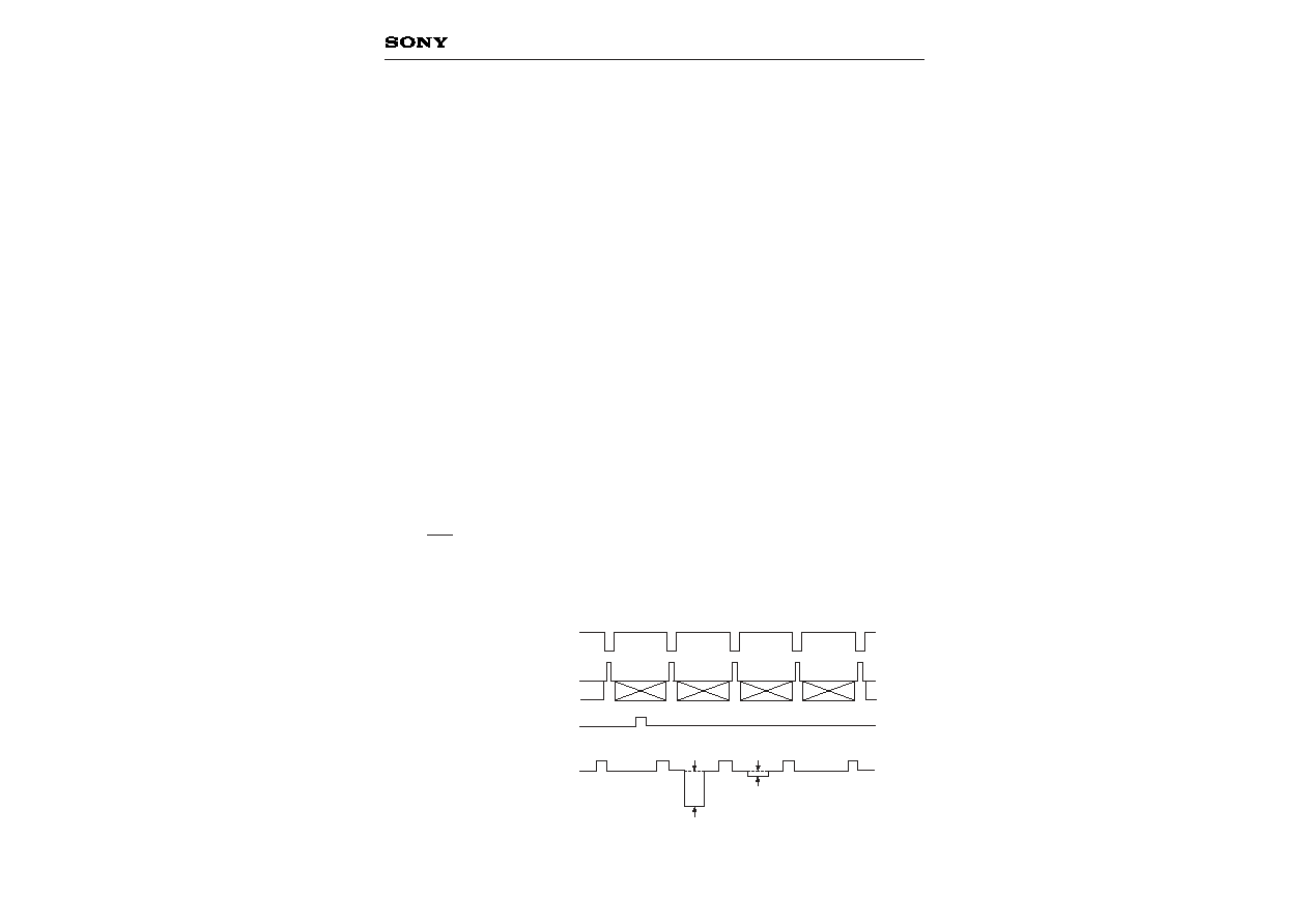
9. Lag
Adjust the Gr signal output value generated by strobe light to 150mV. After setting the strobe light so that it
strobes with the following timing, measure the residual signal (Vlag). Substitute the value into the following
formula.
Lag = (Vlag/150)
◊
100 [%]
VD
V2A
Strobe light timing
Output
Light
signal output 150mV
Vlag (lag)
Gli
Gai

≠ 14 ≠
ICX267AK
Drive Circuit
20
19
15V
XV1
XV2A
XSG1
XSUB
H2
H1
RG
1
2
3
4
5
6
7
8
9
10
19
18
17
16
15
14
13
12
11
CXD1267AN
20
1/35V
100k
H
2
H
1
RG
V
L
NC
GND
V
DD
1
2
3
4
5
6
7
8
9
10
V
1
V
2A
V
2B
V
3
NC
GND
NC
V
OUT
19
18
17
16
15
14
13
12
11
20
ICX267
(Bottom View)
0.1
22/16V
1M 0.1 2200P
22/20V
0.01
3.9k
CCD OUT
2SK523
100
SUB
C
SUB
NC
≠8.0V
XV3
XV2B
XSG2
GND
NC
0.1
1
2
3
4
5
6
7
8
9
10
18
17
16
15
14
13
12
11
CXD1267AN
V
SUB
CONT.
VR1 (1.3K)
Note) Substrate bias control
1. Connect the ground resistor (VR1) shown below to the C
SUB
pin by each readout mode
in order to secure the saturation signal described on the image sensor characteristics.
Progressive scan readout mode
: 2.0k
High frame rate readout mode
: 3.8k
High frame rate 2 pixels addition mode: Ground resistor should not be connected.
2. If the substrate bias control signal is set to high level, and the ground resistor (VR1) connected
to
C
SUB
pin is not grounded at 55ms before the exposure time starts because tf is late, the internal
generation voltage (V
SUB
) may not fall enough.Substrate bias adjustment control signal V
SUB
Cont.
tf
45ms
tr
1ms
GND
Internal generation value V
SUB
(V
SUB
in high frame rate readout
two pixels addition mode)
22/20V
Substrate bias
adjustment control
signal V
SUB
Cont.
Substrate bias
SUB pin voltage

≠ 15 ≠
ICX267AK
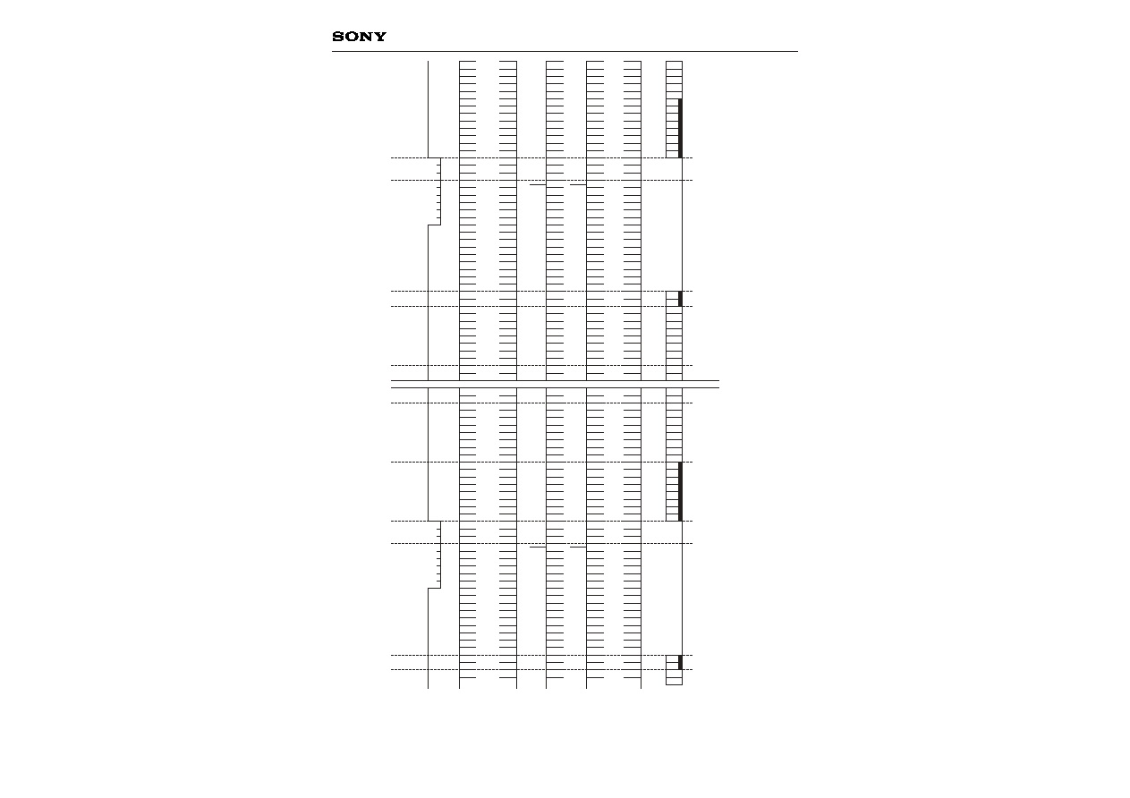
Sensor Readout Clock Timing Chart
Progressive Scan Mode
Progressive Scan Mode (With high-speed sweep)
XV1
XV2A/XV2B
XV3
XSG1
The sensor readout clocks XSG1 and XSG2 are added to each XV2A and XV2B.
HD
V1
V2A
V2B
V3
27.9µs (800 bits)
69.5ns (2 bits)
3.49µs (100 bits)
XSG2

≠ 16 ≠
ICX267AK
Sensor Readout Clock Timing Chart
High Frame Rate Readout Mode
27.9µs (800 bits)
69.5ns (2 bits)
3.49µs (100 bits)
XV1
XV2A/XV2B
XV3
XSG1
HD
V1
V2A
V2B
V3
XSG2
The sensor readout clock XSG2 is added to XV2B.
5.86µs (168 bits)

≠ 17 ≠
ICX267AK
Sensor Readout Clock Timing Chart
High Frame Rate Readout Two Pixels Addition Mode
XV1
XV2A/XV2B
XV3
XSG1
The sensor readout clocks XSG1 and XSG2 are added to each XV2A and XV2B.
HD
V1
V2A
V2B
V3
XSG2
27.9µs (800 bits)
69.5ns (2 bits)
3.49µs (100 bits)
17.15µs (492 bits)
28
98
2
28 28 28 28 28 28 28 28 28 28 28 28 28 2
98
5.86µs (168 bits)
≠ 18 ≠
ICX267AK
Drive Timing Chart (Vertical Sync)
Progressive Scan Mode
VD
HD
1
2
3
4
5
6
7
8
9
10
11
12
21
1
13
1068
1063
1052
1044
1068
1063
V1
V2A
V3
V2B
CCD
OUT
1 2 3 4 5 6 7 8 1 2 3 4 5
1 2 3 4 5 6 7 8 1 2 3 4 5
6 7 8 9 10
1040
1040
1039
1038
≠ 19 ≠
ICX267AK
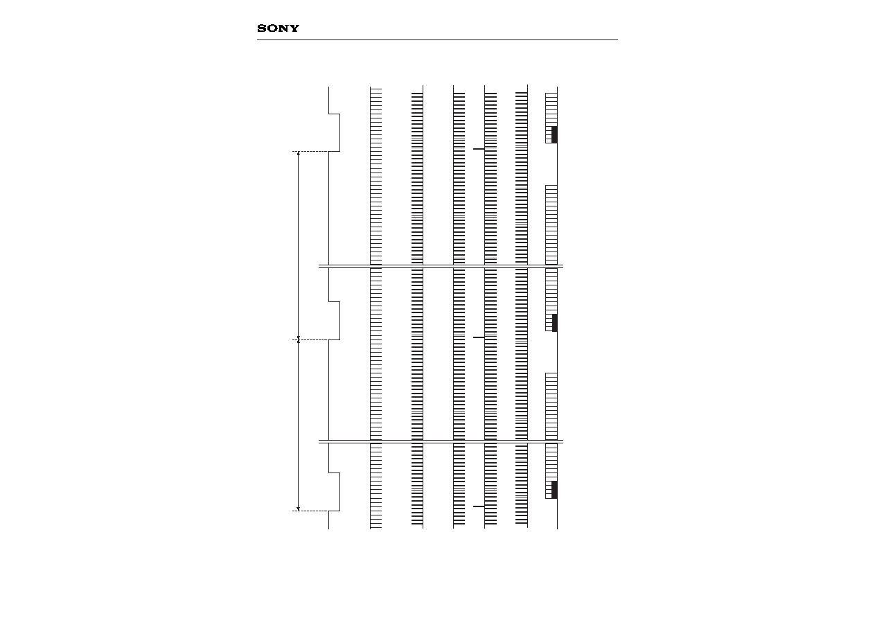
Drive Timing Chart (Vertical Sync)
High Frame Rate Readout Mode
3
4
7
8
3
4
7
8
11
12
15
16
1
2
3
4
5
7
6
8
534
533
532
531
534
533
532
531
530
529
528
527
526
525
524
523
1039
1040
1035
1036
3
4
7
8
3
4
7
8
11
12
15
16
1
2
3
4
5
7
6
8
530
529
528
527
526
525
524
523
1039
1040
1035
1036
V
1
V
2A
V
2B
V
3
CCD
OUT
HD
VD
534
533
532
1
2
3
4
5
7
6
8
531
3
4
7
8
3
4
7
8
11
12
15
16
1/30s
1/30s
≠ 20 ≠
ICX267AK
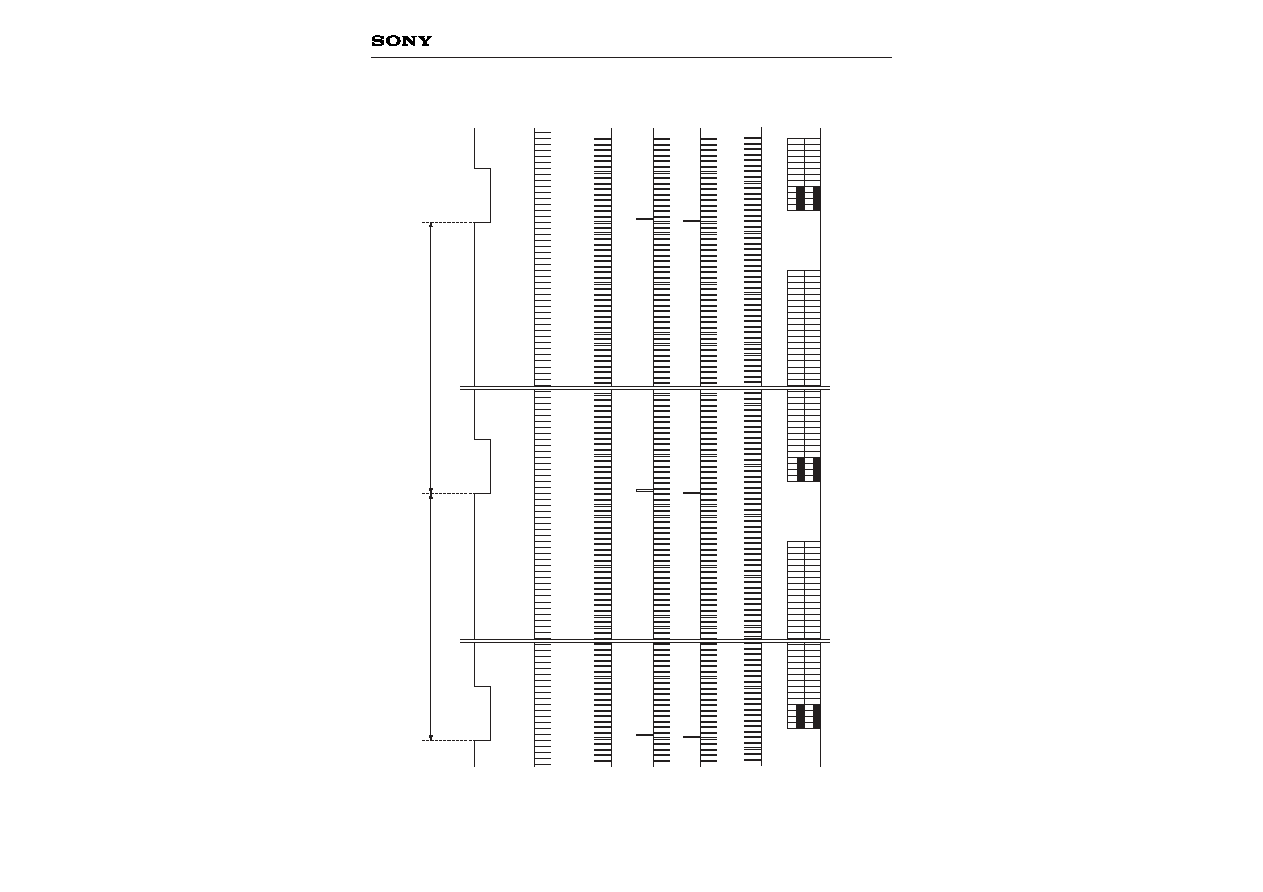
Drive Timing Chart (Vertical Sync)
High Frame Rate Readout Two Pixels Addition Mode
3
4
7
8
3
4
7
8
11
12
15
16
1
2
3
4
5
7
6
8
534
533
532
531
534
533
532
531
530
529
528
527
526
525
524
523
1039
1040
1035
1036
3
4
7
8
3
4
7
8
11
12
15
16
1
2
3
4
5
7
6
8
530
529
528
527
526
525
524
523
1039
1040
1035
1036
V
1
V
2A
V
2B
V
3
CCD
OUT
HD
VD
534
533
532
1
2
3
4
5
7
6
8
531
3
4
7
8
3
4
7
8
11
12
15
16
1/30s
1/30s
1
2
5
6
1
2
5
6
9
10
13
14
1037
1038
1033
1034
1
2
5
6
1
2
5
6
9
10
13
14
1037
1038
1033
1034
1
2
5
6
1
2
5
6
9
10
13
14

≠ 21 ≠
ICX267AK
Drive Timing Chart (Vertical Sync)
Progressive Scan Mode (With high-speed sweep)
RG
V
1
V
2A
V
2B
V
3
SUB
CLK
H
1
H
2
1790
1
56
392
412
430
1
1
1
1
168 1
168
112
56
1
56
56
1
1
112 1
188 1
168
168
1
112
1
1
36
1
112
HD
1
96
16
2

≠ 22 ≠
ICX267AK
Drive Timing Chart (Horizontal Sync)
Progressive Scan Mode
RG
V
1
V
2A
V
2B
V
3
SUB
CLK
H
1
H
2
1790
1
56
392
412
430
HD
1
96
16
2
1
1
1
1
84
28
1
28
1
36
1
84
84
1
1
56
28
1
84
1
56
56
1
84
1
1
112
188
1
84
1
84
84
1
84
1
84
1
84
1
84
1
84
1

≠ 23 ≠
ICX267AK
Drive Timing Chart (Horizontal Sync)
High Frame Rate Readout Mode
RG
V
1
V
2A
V
2B
V
3
SUB
CLK
H
1
H
2
1790
1
56
392
412
430
HD
1
96
16
2
1
1
1
1
84
28
1
28
1
36
1
84
84
1
1
56
28
1
84
1
56
56
1
84
1
1
112
188
1
84
1
84
84
1
84
1
84
1
84
1
84
1
84
1

≠ 24 ≠
ICX267AK
Drive Timing Chart (Horizontal Sync)
High Frame Rate Readout Two Pixels Addition Mode
RG
V
1
V
2A
V
2B
V
3
SUB
CLK
H
1
H
2
1790
1
56
392
412
430
HD
1
96
16
2
1
1
1
1
84
28
1
28
1
36
1
84
84
1
1
56
28
1
84
1
56
56
1
84
1
1
112
188
1
84
1
84
84
1
84
1
84
1
84
1
84
1
84
1
≠ 25 ≠
ICX267AK
Drive Timing Chart (Horizontal Sync)
Progressive Scan Mode (With high-speed sweep) (Refer to "a" on page 21.)
RG
V
1
V
2A
V
2B
V
3
SUB
CLK
H
1
H
2
1790
1
56
392
412
430
1
1
1
1
168 1
168
112
56
1
56
56
1
1
112 1
188 1
168
168
1
112
1
1
36
1
112
HD
1
96
16
2

≠ 26 ≠
ICX267AK
Drive Timing Chart (Horizontal Sync)
Progressive Scan Mode (With high-speed sweep) (Refer to "b" on page 21.)
0/1790
56
56
96
1
1
0/1790
28 28 28 28 28 28
#1
28 28 28 28 28 28
#1470
56
392
392
392
247020 bits = 138 lines
RG
V
1
V
2A
V
2B
V
3
CLK
H
1
H
2
HD
96

≠ 27 ≠
ICX267AK
Notes on Handling
1) Static charge prevention
CCD image sensors are easily damaged by static discharge. Before handling be sure to take the following
protective measures.
a) Either handle bare handed or use non-chargeable gloves, clothes or material.
Also use conductive shoes.
b) When handling directly use an earth band.
c) Install a conductive mat on the floor or working table to prevent the generation of static electricity.
d) Ionized air is recommended for discharge when handling CCD image sensor.
e) For the shipment of mounted substrates, use boxes treated for the prevention of static charges.
2) Soldering
a) Make sure the package temperature does not exceed 80∞C.
b) Solder dipping in a mounting furnace causes damage to the glass and other defects. Use a ground 30W
soldering iron and solder each pin in less than 2 seconds. For repairs and remount, cool sufficiently.
c) To dismount an image sensor, do not use a solder suction equipment. When using an electric desoldering
tool, use a thermal controller of the zero cross On/Off type and connect it to ground.
3) Dust and dirt protection
Image sensors are packed and delivered by taking care of protecting its glass plates from harmful dust and
dirt. Clean glass plates with the following operation as required, and use them.
a) Perform all assembly operations in a clean room (class 1000 or less).
b) Do not either touch glass plates by hand or have any object come in contact with glass surfaces. Should
dirt stick to a glass surface, blow it off with an air blower. (For dirt stuck through static electricity ionized
air is recommended.)
c) Clean with a cotton bud and ethyl alcohol if the grease stained. Be careful not to scratch the glass.
d) Keep in a case to protect from dust and dirt. To prevent dew condensation, preheat or precool when
moving to a room with great temperature differences.
e) When a protective tape is applied before shipping, just before use remove the tape applied for
electrostatic protection. Do not reuse the tape.
4) Installing (attaching)
a) Remain within the following limits when applying a static load to the package. Do not apply any load
more than 0.7mm inside the outer perimeter of the glass portion, and do not apply any load or impact to
limited portions. (This may cause cracks in the package.)
Plastic package
Cover glass
Compressive strength
50N
50N
1.2Nm
Torsional strength
b) If a load is applied to the entire surface by a hard component, bending stress may be generated and
the package may fracture, etc., depending on the flatness of the bottom of the package. Therefore, for
installation, use either an elastic load, such as a spring plate, or an adhesive.

≠ 28 ≠
ICX267AK
c) The adhesive may cause the marking on the rear surface to disappear, especially in case the regulated
voltage value is indicated on the rear surface. Therefore, the adhesive should not be applied to this area,
and indicated values should be transferred to the other locations as a precaution.
d) The notch of the package is used for directional index, and that can not be used for reference of fixing.
In addition, the cover glass and seal resin may overlap with the notch of the package.
e) If the lead bend repeatedly and the metal, etc., clash or rub against the package, the dust may be
generated by the fragments of resin.
f) Acrylate anaerobic adhesives are generally used to attach CCD image sensors. In addition, cyano-acrylate
instantaneous adhesives are sometimes used jointly with acrylate anaerobic adhesives. (reference)
5) Others
a) Do not expose to strong light (sun rays) for long periods, color filters will be discolored. When high
luminance objects are imaged with the exposure level control by electronic-iris, the luminance of the
image-plane may become excessive and discolor of the color filter will possibly be accelerated. In such
a case, it is advisable that taking-lens with the automatic-iris and closing of the shutter during the power-
off mode should be properly arranged. For continuous using under cruel condition exceeding the normal
using condition, consult our company.
b) Exposure to high temperature or humidity will affect the characteristics. Accordingly avoid storage or
usage in such conditions.
c) The brown stain may be seen on the bottom or side of the package. But this does not affect the CCD
characteristics.
d) This package has 2 kinds of internal structure. However, their package outline, optical size, and strength
are the same.
The cross section of lead frame can be seen on the side of the package for structure A.
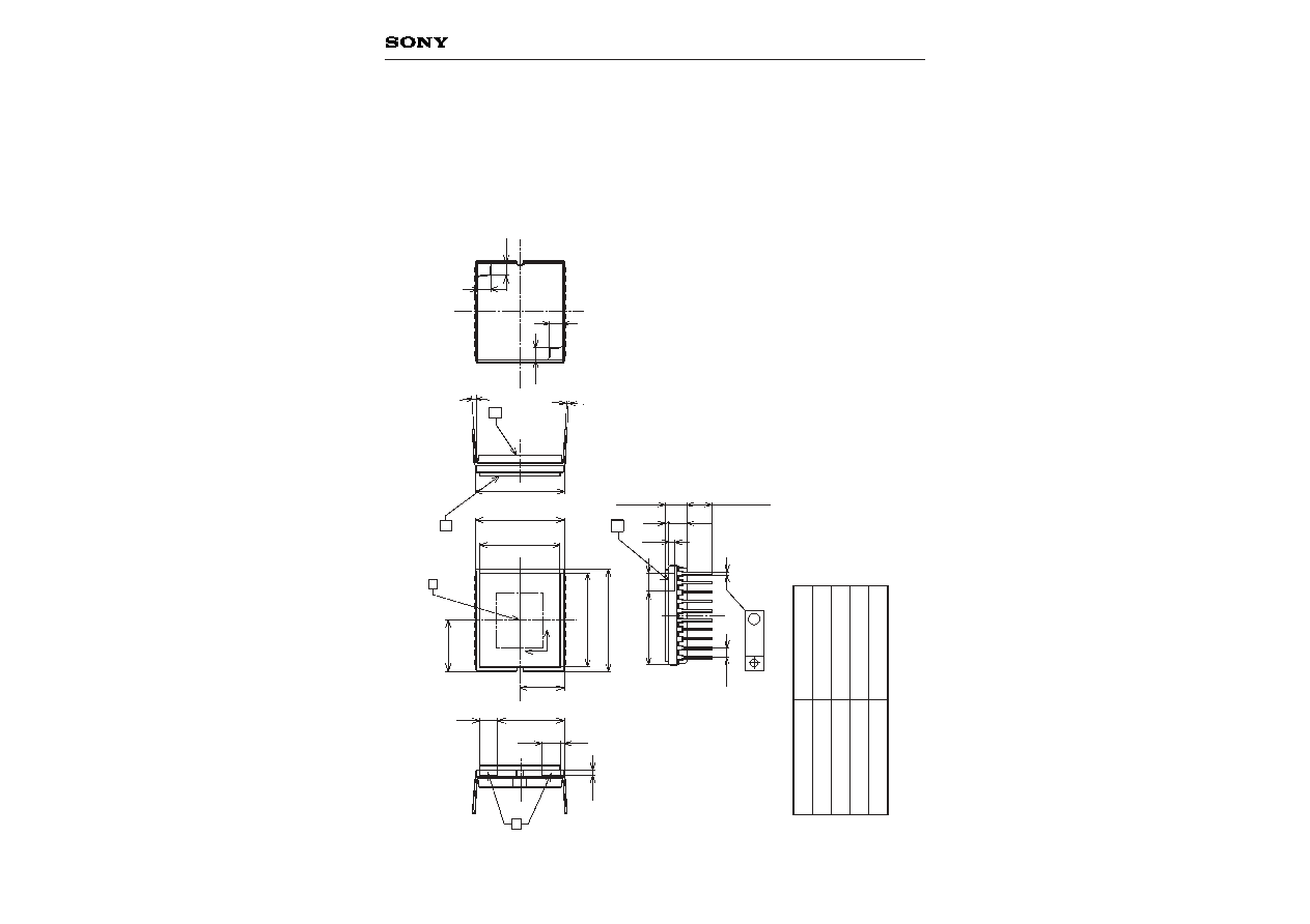
Structure A
Structure B
Chip
Metal plate
(lead frame)
Package
Cross section of
lead frame
≠ 29 ≠
ICX267AK
Package Outline Unit: mm
Son
y Cor
por
ation
20 pin DIP
B
~
B
'
M
A
1
1
C
H
V
D
12.
2
PACKAGE STRUCTURE
PACKAGE MATERIAL
LEAD TREATMENT
LEAD MATERIAL
PACKAGE MASS
DRAWING NUMBER
Plastic
GOLD PLATING
42 ALLOY
AS-B6-04(E)
0.95g
1. "A" is the center of the effective image area.
2. The two points "B" of the package are the horizontal reference.
The point "B'" of the package is the vertical reference.
3. The bottom "C" of the package, and the top of the cover glass "D"
are the height reference.
4. The center of the effective image area relative to "B" and "B'"
is (H, V) = (6.9, 6.0) ± 0.075mm.
5. The rotation angle of the effective image area relative to H and V is ± 1∞.
6. The height from the bottom "C" to the effective image area is 1.41 ± 0.10mm.
The height from the top of the cover glass "D" to the effective image area is 1.49 ± 0.15mm.
7. The tilt of the effective image area relative to the bottom "C" is less than 50µm.
The tilt of the effective image area relative to the top "D" of the cover glass is less than 50µm.
8. The thickness of the cover glass is 0.5mm, and the refractive index is 1.5.
9. The notches on the bottom of the package are used only for directional index, they must
not be used for reference of fixing.
~
~
1.7
11
20
1.7
10
13.8 ± 0.1
12.7
10
20
11
6.9
10.9
0.8
1.27
0.3
0.3
10.0
2.5
0∞ to 9∞
0.5
2.5
9.0
2.5
6.0
12.0 ± 0.1
0.25
1.7
1.7
0.8
0.5
2.9 ± 0.15
2.4
3.5 ± 0.3