 | –≠–ª–µ–∫—Ç—Ä–æ–Ω–Ω—ã–π –∫–æ–º–ø–æ–Ω–µ–Ω—Ç: ICX284AK | –°–∫–∞—á–∞—Ç—å:  PDF PDF  ZIP ZIP |
Diagonal 6.64mm (Type 1/2.7) Frame Readout CCD Image Sensor with Square Pixel for Color Cameras
Description
The ICX284AK is a diagonal 6.64mm (Type 1/2.7)
interline CCD solid-state image sensor with a square
pixel array and 2.02M effective pixels. Frame
readout allows all pixels' signals to be output
independently within approximately 1/7.5 second.
Also, the adoption of high frame rate readout mode
supports 30 frames per second which is four times
the speed in frame readout mode. This chip features
an electronic shutter with variable charge-storage
time. Adoption of a design specially suited for frame
readout ensures a saturation signal level equivalent
to when using field readout. Ye, Cy, Mg, G
complementary color mosaic filters are used as the
color filters, and at the same time high sensitivity and
low dark current are achieved through the adoption
of Super HAD CCD technology.
This chip is suitable for applications such as electronic
still cameras, PC input cameras, etc.
Features
∑ Supports frame readout
∑ High horizontal and vertical resolution
∑ Supports high frame rate readout mode: 30 frames/s
∑ Square pixel
∑ Horizontal drive frequency: 18MHz
∑ No voltage adjustments (reset gate and substrate bias are not adjusted.)
∑ Ye, Cy, Mg, G complementary color mosaic filters on chip
∑ High sensitivity, low smear
∑ Continuous variable-speed shutter
∑ Low dark current, excellent anti-blooming characteristics
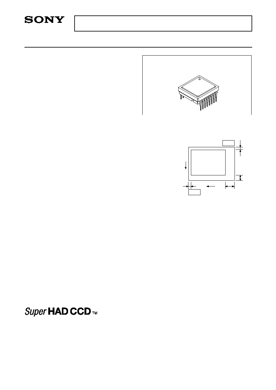
∑ 16-pin high-precision plastic package (top/bottom dual surface reference possible)
Device Structure
∑ Interline CCD image sensor
∑ Image size:
Diagonal 6.64mm (Type 1/2.7)
∑ Total number of pixels:
1688 (H)
◊
1248 (V) approx. 2.11M pixels
∑ Number of effective pixels: 1636 (H)
◊
1236 (V) approx. 2.02M pixels
∑ Number of active pixels:
1620 (H)
◊
1220 (V) approx. 1.98M pixels
∑ Chip size:
6.17mm (H)
◊
5.17mm (V)
∑ Unit cell size:
3.275µm (H)
◊
3.275µm (V)
∑ Optical black:
Horizontal (H) direction: Front 4 pixels, rear 48 pixels
Vertical (V) direction:
Front 10 pixels, rear 2 pixels
∑ Number of dummy bits:
Horizontal 28
Vertical 1 (even fields only)
∑ Substrate material:
Silicon
≠ 1 ≠
E99410-PS
Sony reserves the right to change products and specifications without prior notice. This information does not convey any license by
any implication or otherwise under any patents or other right. Application circuits shown, if any, are typical examples illustrating the
operation of the devices. Sony cannot assume responsibility for any problems arising out of the use of these circuits.
ICX284AK
16 pin DIP (Plastic)
Super HAD CCD is a trademark of Sony Corporation. Super HAD CCD is a CCD that drastically improves sensitivity by introducing newly
developed semiconductor technology by Sony Corporation into Sony's high-performance HAD (Hole-Accumulation Diode) sensor.
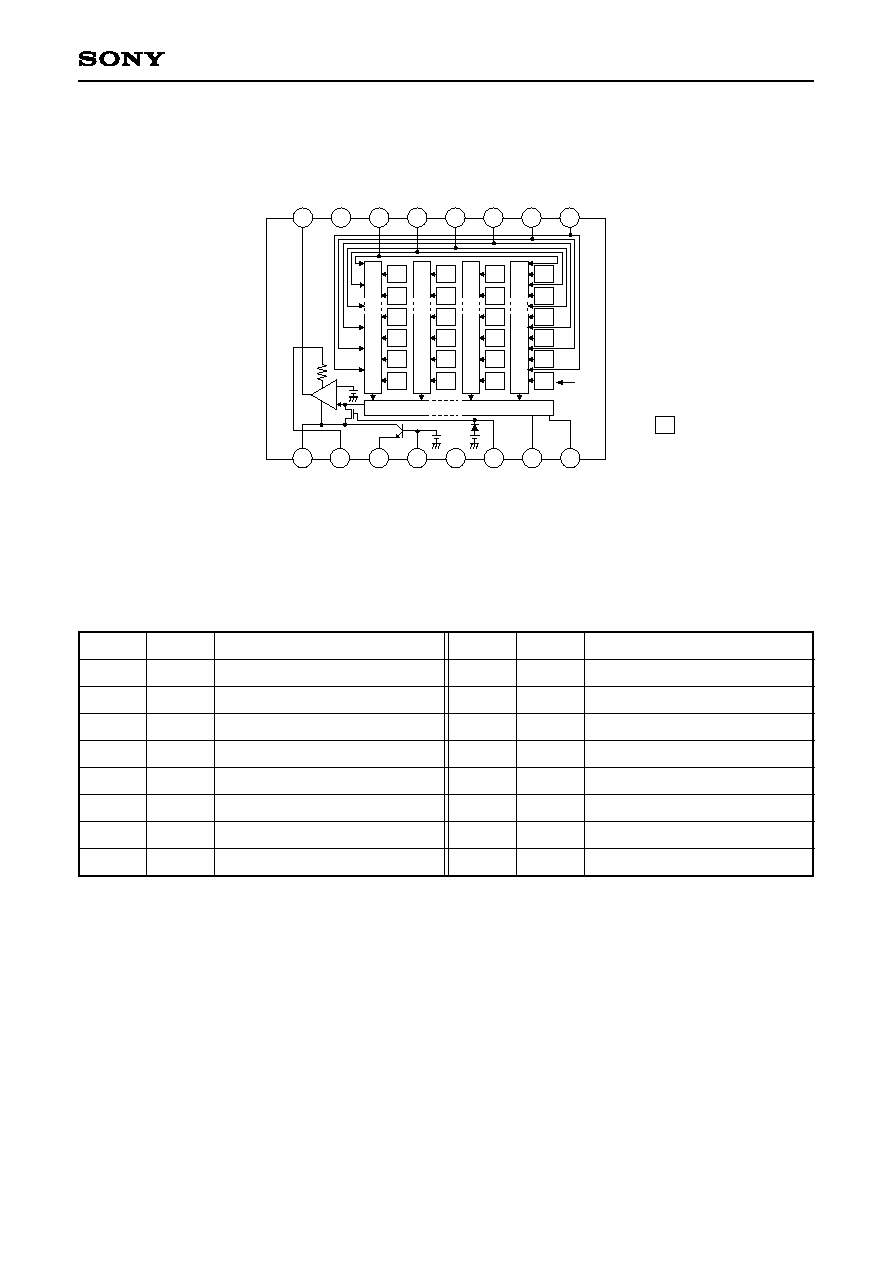
Pin 1
V
4
48
2
10
Pin 9
H
Optical black position
(Top View)
≠ 2 ≠
ICX284AK
Note)
: Photo sensor
V
O
U
T
G
N
D
V
1
B
V
1
A
V
2
V
3
B
V
3
A
V
4
V
D
D
G
N
D
S
U
B
C
S
U
B
V
L
R
G
H
1
H
2
Cy
Mg
Cy
Mg
Cy
Mg
Ye
G
Ye
G
Ye
G
Cy
Mg
Cy
Mg
Cy
Mg
Ye
G
Ye
G
Ye
G
Horizontal register
Note)
2
3
4
5
6
7
8
9
10
11
12
13
14
15
16
1
V
e
r
t
i
c
a
l
r
e
g
i
s
t
e
r
Block Diagram and Pin Configuration
(Top View)
Pin Description
1
DC bias is generated within the CCD, so that this pin should be grounded externally through a capacitance
of 0.1µF.
Pin No.
Symbol
Description
Pin No.
Symbol
Description
1
2
3
4
5
6
7
8
V
4
V
3A
V
3B
V
2
V
1A
V
1B
GND
V
OUT
Vertical register transfer clock
Vertical register transfer clock
Vertical register transfer clock
Vertical register transfer clock
Vertical register transfer clock
Vertical register transfer clock
GND
Signal output
9
10
11
12
13
14
15
16
V
DD
GND
SUB
C
SUB
V
L
RG
H
1
H
2
Supply voltage
GND
Substrate clock
Substrate bias
1
Protective transistor bias
Reset gate clock
Horizontal register transfer clock
Horizontal register transfer clock
≠ 3 ≠
ICX284AK
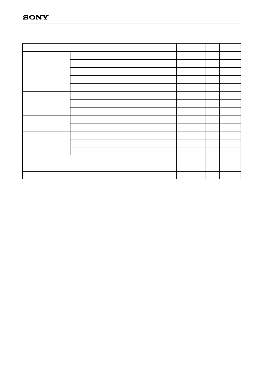
Absolute Maximum Ratings
≠40 to +12
≠50 to +15
≠50 to +0.3
≠40 to +0.3
≠25 to
≠0.3 to +22
≠10 to +18
≠10 to +6.5
≠0.3 to +28
≠0.3 to +15
to +15
≠6.5 to +6.5
≠10 to +16
≠30 to +80
≠10 to +60
≠10 to +75
V
V
V
V
V
V
V
V
V
V
V
V
V
∞C
∞C
∞C
V
DD
, V
OUT
,
RG ≠
SUB
V
1A
, V
1B
, V
3A
, V
3B
≠
SUB
V
2
, V
4
, V
L
≠
SUB
H
1
, H
2
, GND ≠
SUB
C
SUB
≠
SUB
V
DD
, V
OUT
,
RG, C
SUB
≠ GND
V
1A
, V
1B
, V
2
, V
3A
, V
3B
, V
4
≠ GND
H
1
, H
2
≠ GND
V
1A
, V
1B
, V
3A
, V
3B
≠ V
L
V
2
, V
4
, H
1
, H
2
, GND ≠ V
L
Voltage difference between vertical clock input pins
H
1
≠ H
2
H
1
, H
2
≠ V
4
Item
Ratings
Unit
Remarks
2
+24V (Max.) when clock width < 10µs, clock duty factor < 0.1%.
+16V (Max.) is guaranteed for turning on or off power supply.
2
Against
SUB
Against GND
Against V
L
Between input clock
pins
Storage temperature
Guaranteed temperature of performance
Operating temperature
≠ 4 ≠
ICX284AK
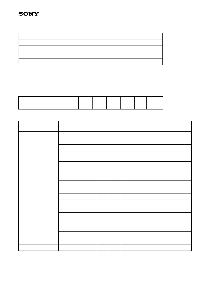
Clock Voltage Conditions
Item
Readout clock voltage
V
VT
V
VH1
, V
VH2
V
VH3
, V
VH4
V
VL1
, V
VL2
,
V
VL3
, V
VL4
V
V
V
VH3
≠ V
VH
V
VH4
≠ V
VH
V
VHH
V
VHL
V
VLH
V
VLL
V
H
V
HL
V
CR
V
RG
V
RGLH
≠ V
RGLL
V
RGL
≠ V
RGLm
V
SUB
14.55
≠0.05
≠0.2
≠8.0
6.8
≠0.25
≠0.25
3.0
≠0.05
0.5
3.0
21.5
15.0
0
0
≠7.5
7.5
3.3
0
1.65
3.3
22.5
15.45
0.05
0.05
≠7.0
8.05
0.1
0.1
0.5
0.5
0.5
0.5
3.6
0.05
3.6
0.4
0.5
23.5
V
V
V
V
V
V
V
V
V
V
V
V
V
V
V
V
V
V
1
2
2
2
2
2
2
2
2
2
2
3
3
3
4
4
4
5
V
VH
= (V
VH1
+ V
VH2
)/2
V
VL
= (V
VL3
+ V
VL4
)/2
V
V
= V
VH
n ≠ V
VL
n (n = 1 to 4)
High-level coupling
High-level coupling
Low-level coupling
Low-level coupling
Cross-point voltage
Low-level coupling
Low-level coupling
Horizontal transfer
clock voltage
Reset gate clock
voltage
Substrate clock voltage
Vertical transfer clock
voltage
Symbol
Min.
Typ.
Max.
Unit
Remarks
Bias Conditions
Item
Supply voltage
Protective transistor bias
Substrate clock
Reset gate clock
V
DD
V
L
SUB
RG
14.55
15.0
1
2
2
15.45
V
Symbol
Min.
Typ.
Max.
Unit
Remarks
DC Characteristics
Item
Supply current
I
DD
6.5
mA
Symbol
Min.
Typ.
Max.
Unit
Remarks
1
V
L
setting is the V
VL
voltage of the vertical transfer clock waveform, or the same voltage as the V
L
power
supply for the V driver should be used.
2
Do not apply a DC bias to the substrate clock and reset gate clock pins, because a DC bias is generated
within the CCD.
Waveform
diagram
≠ 5 ≠
ICX284AK
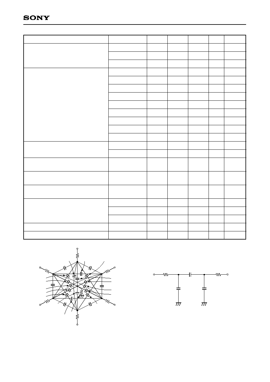
Clock Equivalent Circuit Constant
Item
Capacitance between vertical transfer
clock and GND
C
V1A
, C
V3A
C
V1B
, C
V3B
C
V2
, C
V4
C
V1A2
, C
V3A4
C
V1B2
, C
V3B4
C
V23A
, C
V41A
C
V23B
, C
V41B
C
V1A3A
C
V1B3B
C
V1A3B
, C
V1B3A
C
V24
C
V1A1B
, C
V3A3B
C
H1
C
H2
C
HH
C
RG
C
SUB
R
1A
, R
3A
R
1B
, R
3B
R
2
, R
4
R
GND
R
H
390
1200
1500
120
470
62
120
12
91
30
91
30
47
47
68
5
620
56
62
91
18
5
pF
pF
pF
pF
pF
pF
pF
pF
pF
pF
pF
pF
pF
pF
pF
pF
pF
Capacitance between vertical transfer
clocks
Capacitance between horizontal transfer
clock and GND
Capacitance between horizontal transfer
clocks
Capacitance between reset gate clock
and GND
Capacitance between substrate clock
and GND
Vertical transfer clock series resistor
Vertical transfer clock ground resistor
Horizontal transfer clock series resistor
Symbol
Min.
Typ.
Max.
Unit
Remarks
R
GND
C
V1B3B
R
1B
C
V41B
V
1B
C
V4
C
V41A
C
V1B
C
V1B3A
C
V1A1B
C
V1A
C
V1B2
R
1A
V
1A
C
V1A2
V
2
R
2
C
V24
C
V1A3A
C
V23A
C
V23B
R
3A
V
3A
C
V2
C
V3A
C
V3A3B
C
V1A3B
C
V3B
R
3B
V
3B
C
V3A4
C
V3B4
V
4
R
4
Vertical transfer clock equivalent circuit
H
1
R
H
C
H1
C
H2
R
H
C
HH
H
2
Horizontal transfer clock equivalent circuit