 | –≠–ª–µ–∫—Ç—Ä–æ–Ω–Ω—ã–π –∫–æ–º–ø–æ–Ω–µ–Ω—Ç: ICX406AQF | –°–∫–∞—á–∞—Ç—å:  PDF PDF  ZIP ZIP |
≠ 1 ≠
E01331-PS
Sony reserves the right to change products and specifications without prior notice. This information does not convey any license by
any implication or otherwise under any patents or other right. Application circuits shown, if any, are typical examples illustrating the
operation of the devices. Sony cannot assume responsibility for any problems arising out of the use of these circuits.
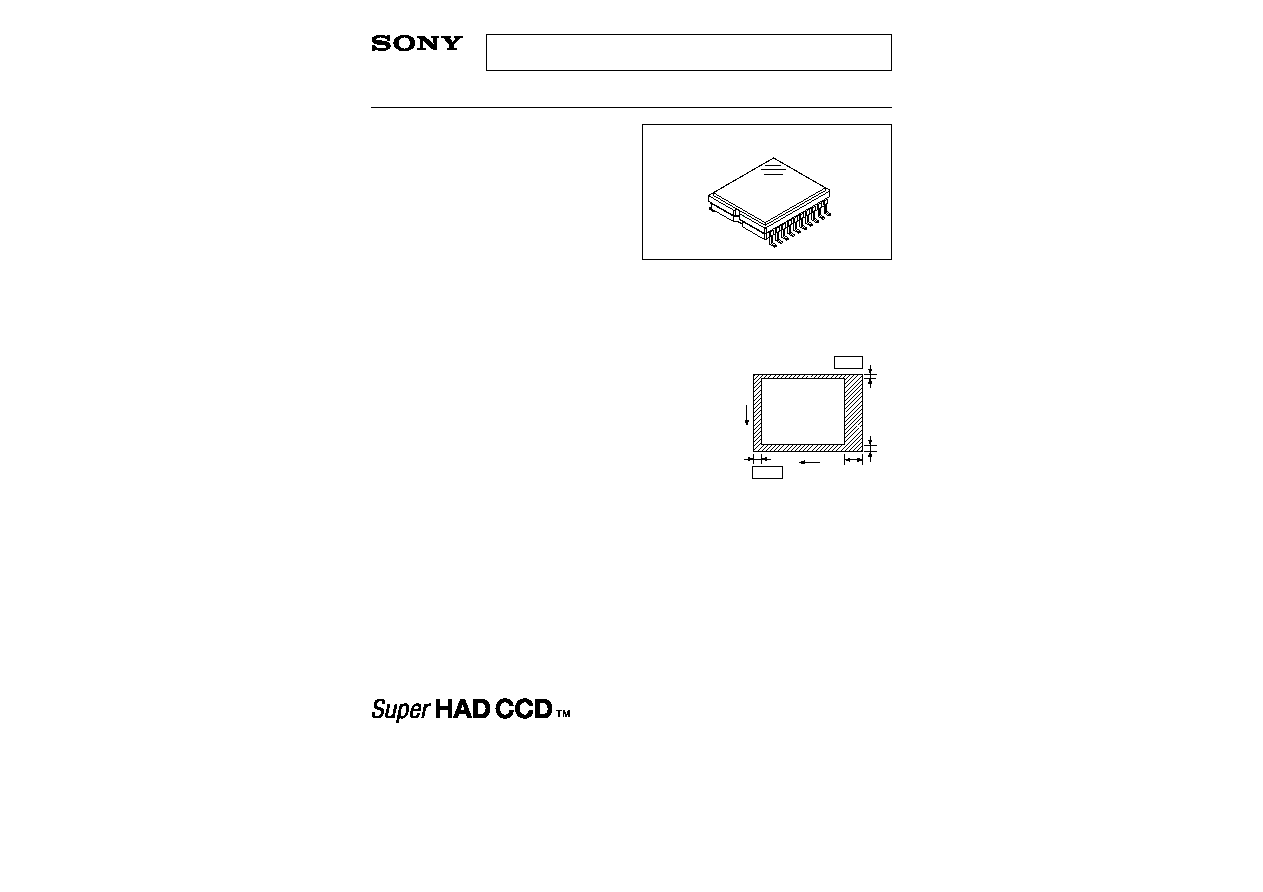
ICX406AQF
20 pin SOP (Plastic)
Description
The ICX406AQF is a diagonal 8.98mm (Type 1/1.8)
interline CCD solid-state image sensor with a square
pixel array and 3.98M effective pixels. Frame readout
allows all pixels' signals to be output independently
within approximately 1/3.33 second.
Also, number of vertical pixels decimation allows
output of 30 frames per second in high frame rate
readout mode.
This chip features an electronic shutter with
variable charge-storage time.
R, G, B primary color mosaic filters are used as the
color filters, and at the same time high sensitivity and
low dark current are achieved through the adoption
of Super HAD CCD technology.
This chip is suitable for applications such as
electronic still cameras, etc.
Features
∑ Supprots frame readout
∑ High horizontal and vertical resolution
∑ Supports high frame rate readout mode: 30 frames/s, 25 frames/s,
AF1 mode: 60 frames/s, 50 frames/s,
AF2 mode: 120 frames/s, 100 frames/s
∑ Square pixel
∑ Horizontal drive frequency: 18MHz
∑ No voltage adjustments (reset gate and substrate bias are not adjusted.)
∑ R, G, B primary color mosaic filters on chip
∑ High sensitivity, low dark current
∑ Continuous variable-speed shutter
∑ Excellent anti-blooming characteristics
∑ Exit pupil distance recommended range ≠20 to ≠100mm
∑ 20-pin high-precision plastic package
Device Structure
∑ Interline CCD image sensor
∑ Total number of pixels:
2384 (H)
◊
1734 (V) approx. 4.13M pixels
∑ Number of effective pixels:
2312 (H)
◊
1720 (V) approx. 3.98M pixels
∑ Number of active pixels:
2308 (H)
◊
1712 (V) approx. 3.95M pixels diagonal 8.980mm
∑ Number of recommended recording pixels:
2272 (H)
◊
1740 (V) approx. 3.87M pixels diagonal 8.875mm aspect ratio 4:3
∑ Chip size:
8.10mm (H)
◊
6.64mm (V)
∑ Unit cell size:
3.125µm (H)
◊
3.125µm (V)
∑ Optical black:
Horizontal (H) direction: Front 16 pixels, rear 56 pixels
Vertical (V) direction:
Front 12 pixels, rear 2 pixels
∑ Number of dummy bits:
Horizontal 28
Vertical 1 (even fields only)
∑ Substrate material:
Silicon
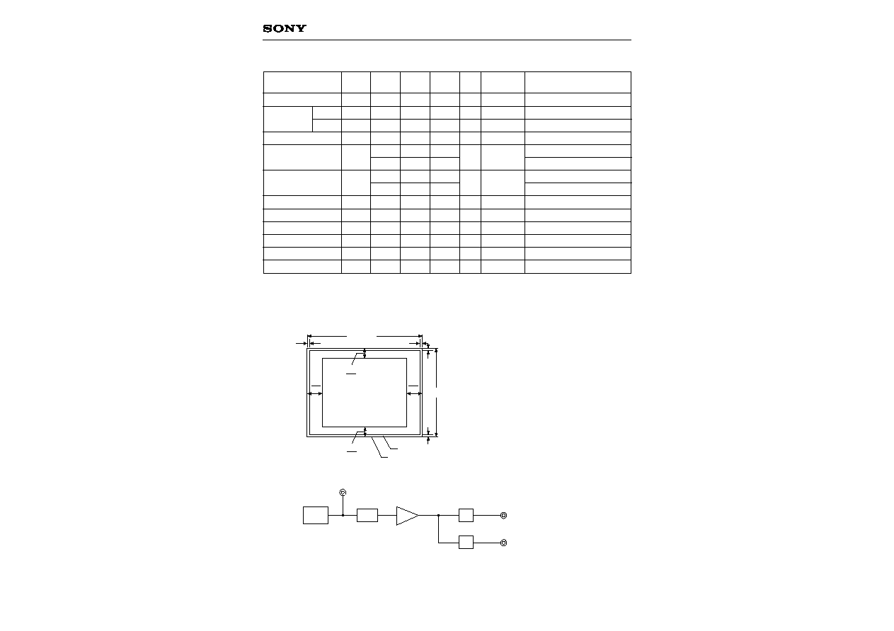
Diagonal 8.98mm (Type 1/1.8) Frame Readout CCD Image Sensor with a Square Pixel for Color Cameras
Optical black position
(Top View)
2
12
V
H
Pin 1
Pin 11
56
16
Super HAD CCD is a trademark of Sony Corporation. The Super HAD CCD is a version of Sony's high performance CCD HAD (Hole-
Accumulation Diode) sensor with sharply improved sensitivity by the incorporation of a new semiconductor technology developed by Sony
Corporation.
≠ 2 ≠
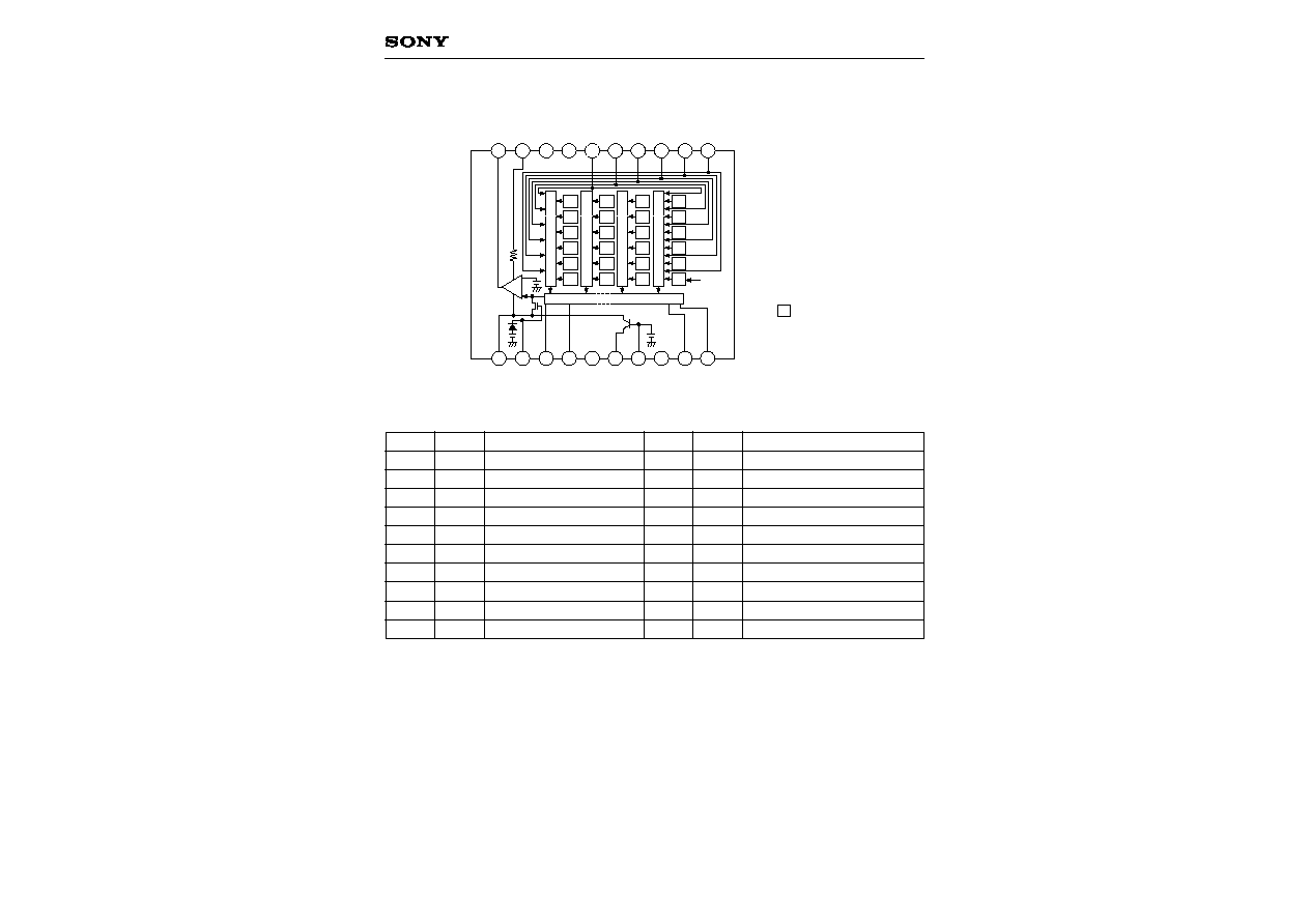
ICX406AQF
11
12
13
14
15
16
17
18
19
20
Note)
Note) : Photo sensor
Horizontal register
V
e
r
tical register
V
DD
RG
H
2
H
1
GND
SUB
C
SUB
V
L
H
1
H
2
10
9
8
7
6
5
4
3
2
1
V
OUT
GND
TEST
TEST
V
1B
V
1A
V
2
V
3B
V
3A
V
4
B
Gr
B
Gr
B
Gb
R
Gb
R
Gb
B
Gr
B
Gr
B
Gb
R
Gb
R
Gb
Gr
R
Gr
R
Block Diagram and Pin Configuration
(Top View)
Pin No.
Symbol
Description
Pin No.
Symbol
Description
1
2
3
4
5
6
7
8
9
10
V
4
V
3A
V
3B
V
2
V
1A
V
1B
TEST
TEST
GND
V
OUT
Vertical register transfer clock
Vertical register transfer clock
Vertical register transfer clock
Vertical register transfer clock
Vertical register transfer clock
Vertical register transfer clock
Test pin
1
Test pin
1
GND
Signal output
11
12
13
14
15
16
17
18
19
20
V
DD
RG
H
2
H
1
GND
SUB
C
SUB
V
L
H
1
H
2
Supply voltage
Reset gate clock
Horizontal register transfer clock
Horizontal register transfer clock
GND
Substrate clock
Substrate bias
2
Protective transistor bias
Horizontal register transfer clock
Horizontal register transfer clock
Pin Description
1
Leave this pin open.
2
DC bias is generated within the CCD, so that this pin should be grounded externally through a capacitance
of 0.1µF.
≠ 3 ≠
ICX406AQF
Absolute Maximum Ratings
Item
V
DD
, V
OUT
,
RG ≠
SUB
V
1A
, V
1B
, V
3A
, V
3B
≠
SUB
V
2
, V
4
, V
L
≠
SUB
H
1
, H
2
, GND ≠
SUB
C
SUB
≠
SUB
V
DD
, V
OUT
,
RG, C
SUB
≠ GND
V
1A
, V
1B
, V
2
, V
3A
, V
3B
, V
4
≠ GND
H
1
, H
2
≠ GND
V
1A
, V
1B
, V
3A
, V
3B
≠ V
L
V
2
, V
4
, H
1
, H
2
, GND ≠ V
L
Voltage difference between vertical clock input pins
H
1
≠ H
2
H
1
, H
2
≠ V
4
Against
SUB
Against GND
Against V
L
Between input
clock pins
Storage temperature
Guaranteed temperature of performance
Operating temperature
≠40 to +12
≠50 to +15
≠50 to +0.3
≠40 to +0.3
≠25 to
≠0.3 to +22
≠10 to +18
≠10 to +6.5
≠0.3 to +28
≠0.3 to +15
to +15
≠6.5 to +6.5
≠10 to +16
≠30 to +80
≠10 to +60
≠10 to +75
V
V
V
V
V
V
V
V
V
V
V
V
V
∞C
∞C
∞C
1
Ratings
Unit
Remarks
1
+24V (Max.) when clock width < 10µs, clock duty factor < 0.1%.
+16V (Max.) is guaranteed for turning on or off power supply.
≠ 4 ≠
ICX406AQF
Bias Conditions
Supply voltage
Protective transistor bias
Substrate clock
Reset gate clock
Item
V
DD
V
L
SUB
RG
Symbol
15.0
1
2
2
Min.
V
Unit
Remarks
Typ.
Max.
1
V
L
setting is the V
VL
voltage of the vertical clock waveform, or the same voltage as the V
L
power supply
for the V driver should be used.
2
Do not apply a DC bias to the substrate clock and reset gate clock pins, because a DC bias is generated
within the CCD.
DC Characteristics
14.55
15.45
Supply current
Item
I
DD
Symbol
7.0
Min.
Unit
Remarks
Typ.
Max.
mA
10.0
3.0
Clock Voltage Conditions
Item
Symbol
Min.
Typ.
Max. Unit
Waveform
Diagram
Remarks
Readout clock voltage
Vertical transfer clock
voltage
Horizontal transfer
clock voltage
Reset gate clock
voltage
Substrate clock voltage
V
VT
V
VH1
, V
VH2
V
VH3
, V
VH4
V
VL1
, V
VL2
,
V
VL3
, V
VL4
V
V
V
VH3
≠ V
VH
V
VH4
≠ V
VH
V
VHH
V
VHL
V
VLH
V
VLL
V
H
V
HL
V
CR
V
RG
V
RGLH
≠ V
RGLL
V
RGL
≠ V
RGLm
V
SUB
14.55
≠0.05
≠0.2
≠8.0
6.8
≠0.25
≠0.25
4.75
≠0.05
0.8
3.0
21.5
15.0
0
0
≠7.5
7.5
5.0
0
2.5
3.3
22.5
15.45
0.05
0.05
≠7.0
8.05
0.1
0.1
0.9
0.9
0.9
0.7
5.25
0.05
5.25
0.4
0.5
23.5
1
2
2
2
2
2
2
2
2
2
2
3
3
3
4
4
4
5
V
VH
= (V
VH1
+ V
VH2
)/2
V
VL
= (V
VL3
+ V
VL4
)/2
V
V
= V
VH
n ≠ V
VL
n (n = 1 to 4)
High-level coupling
High-level coupling
Low-level coupling
Low-level coupling
Cross-point voltage
Low-level coupling
Low-level coupling
V
V
V
V
V
V
V
V
V
V
V
V
V
V
V
V
V
V
≠ 5 ≠
ICX406AQF
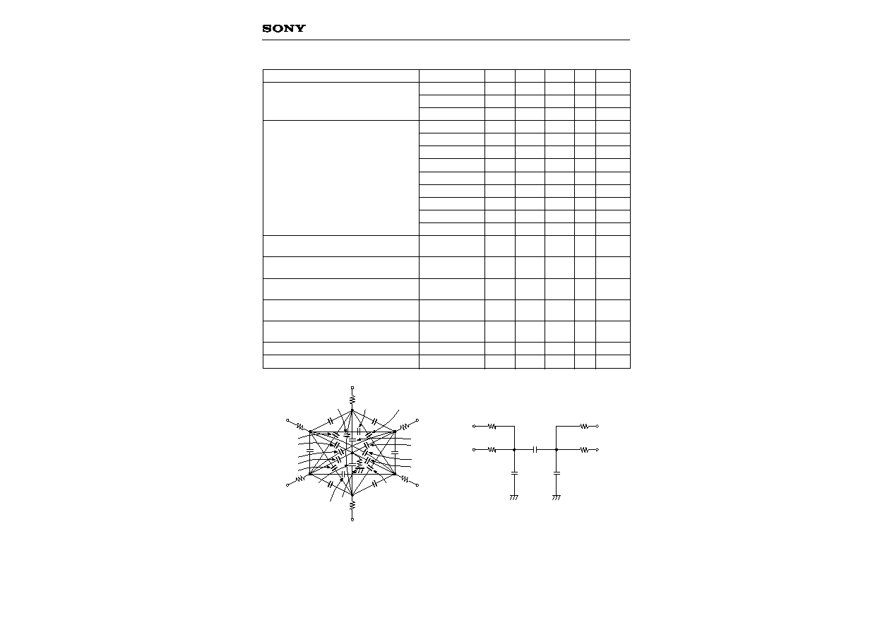
Clock Equivalent Circuit Constants
C
V1A
, C
V3A
C
V1B
, C
V3B
C
V2
, C
V4
C
V1A2
, C
V3A4
C
V1B2
, C
V3B4
C
V23A
, C
V41A
C
V23B
, C
V41B
C
V1A3A
C
V1B3B
C
V1A3B
, C
V1B3A
C
V24
C
V1A1B
, C
V3A3B
C
H1
, C
H2
C
HH
C
RG
C
SUB
R
1A
, R
1B
, R
2
,
R
3A
, R
3B
, R
4
R
GND
R
H
Symbol
Capacitance between vertical transfer clock
and GND
Capacitance between vertical transfer
clocks
Capacitance between horizontal transfer
clock and GND
Capacitance between horizontal transfer
clocks
Capacitance between reset gate clock and
GND
Capacitance between substrate clock and
GND
Vertical transfer clock series resistor
Vertical transfer clock ground resistor
Horizontal transfer clock series resistor
Item
Min.
1200
4700
3300
470
560
150
220
39
220
56
82
68
36
91
8
1000
62
18
15
Typ.
Max.
pF
pF
pF
pF
pF
pF
pF
pF
pF
pF
pF
pF
pF
pF
pF
pF
Unit Remarks
Vertical transfer clock equivalent circuit
Horizontal transfer clock equivalent circuit
H
1
H
2
C
H1
C
H2
C
HH
R
H
R
H
H
1
H
2
R
H
R
H
R
GND
C
V1B3B
R
1B
C
V41B
V
1B
C
V4
C
V41A
C
V1B
C
V1B3A
C
V1A1B
C
V1A
C
V1B2
R
1A
V
1A
C
V1A2
V
2
R
2
C
V24
C
V1A3A
C
V23A
C
V23B
R
3A
V
3A
C
V2
C
V3A
C
V3A3B
C
V1A3B
C
V3B
R
3B
V
3B
C
V3A4
C
V3B4
V
4
R
4
≠ 6 ≠
ICX406AQF
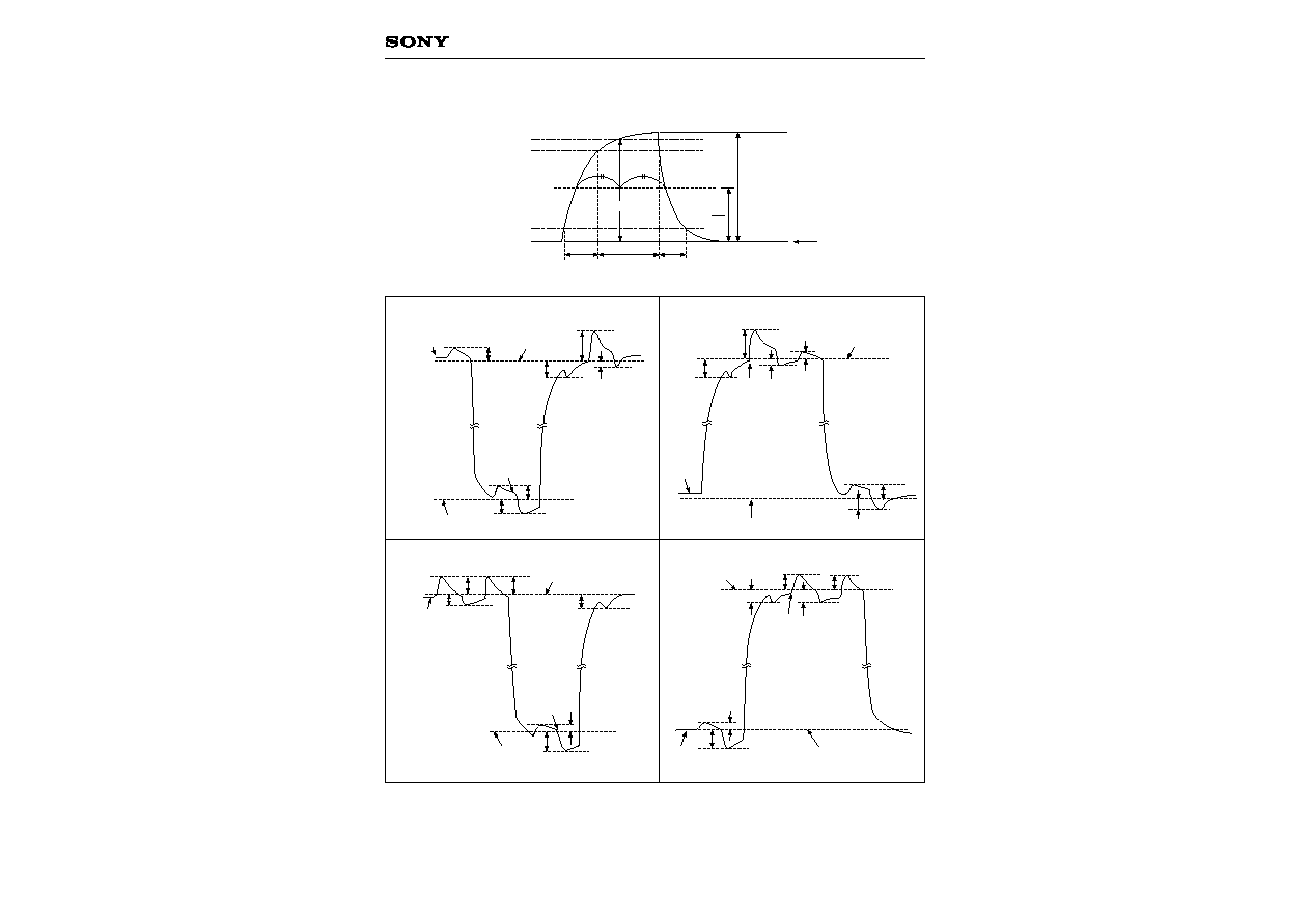
Drive Clock Waveform Conditions
(1) Readout clock waveform
V
VH
= (V
VH1
+ V
VH2
)/2
V
VL
= (V
VL3
+ V
VL4
)/2
V
V
= V
VH
n ≠ V
VL
n (n = 1 to 4)
(2) Vertical transfer clock waveform
100%
90%
10%
0%
tr
tf
0V
twh
M
2
M
V
VT
V
VH1
V
VHH
V
VHL
V
VH
V
VLH
V
VL1
V
VLL
V
VHL
V
VHH
V
VL
V
VH2
V
VHH
V
VHH
V
VHL
V
VHL
V
VH
V
VLH
V
VL2
V
VLL
V
VL
V
VHH
V
VH
V
VLH
V
VLL
V
VL
V
VHL
V
VL3
V
VHL
V
VH3
V
VHH
V
VH
V
VL
V
VHL
V
VLH
V
VLL
V
VHL
V
VH4
V
VHH
V
VHH
V
VL4
V
1A
, V
1B
V
3A
, V
3B
V
2
V
4
≠ 7 ≠
ICX406AQF
V
HL
V
CR
twl
two
twh
V
H
V
H
2
tr
H
2
90%
10%
H
1
tf
RG waveform
V
RGLH
V
RGH
V
RGL
V
RGLL
V
RGLm
tr
twh
twl
tf
V
RG
Point A
V
SUB
(A bias generated within the CCD)
100%
90%
10%
0%
tr
tf
twh
M
2
M
V
SUB
(3) Horizontal transfer clock waveform
Cross-point voltage for the H
1
rising side of the horizontal transfer clocks H
1
and H
2
waveforms is V
CR
.
The overlap period for twh and twl of horizontal transfer clocks H
1
and H
2
is two.
(4) Reset gate clock waveform
V
RGLH
is the maximum value and V
RGLL
is the minimum value of the coupling waveform during the period from
Point A in the above diagram until the rising edge of RG.
In addition, V
RGL
is the average value of V
RGLH
and V
RGLL
.
V
RGL
= (V
RGLH
+ V
RGLL
)/2
Assuming V
RGH
is the minimum value during the interval with twh, then:
V
RG
= V
RGH
≠ V
RGL
Negative overshoot level during the falling edge of RG is V
RGLm
.
(5) Substrate clock waveform
≠ 8 ≠
ICX406AQF
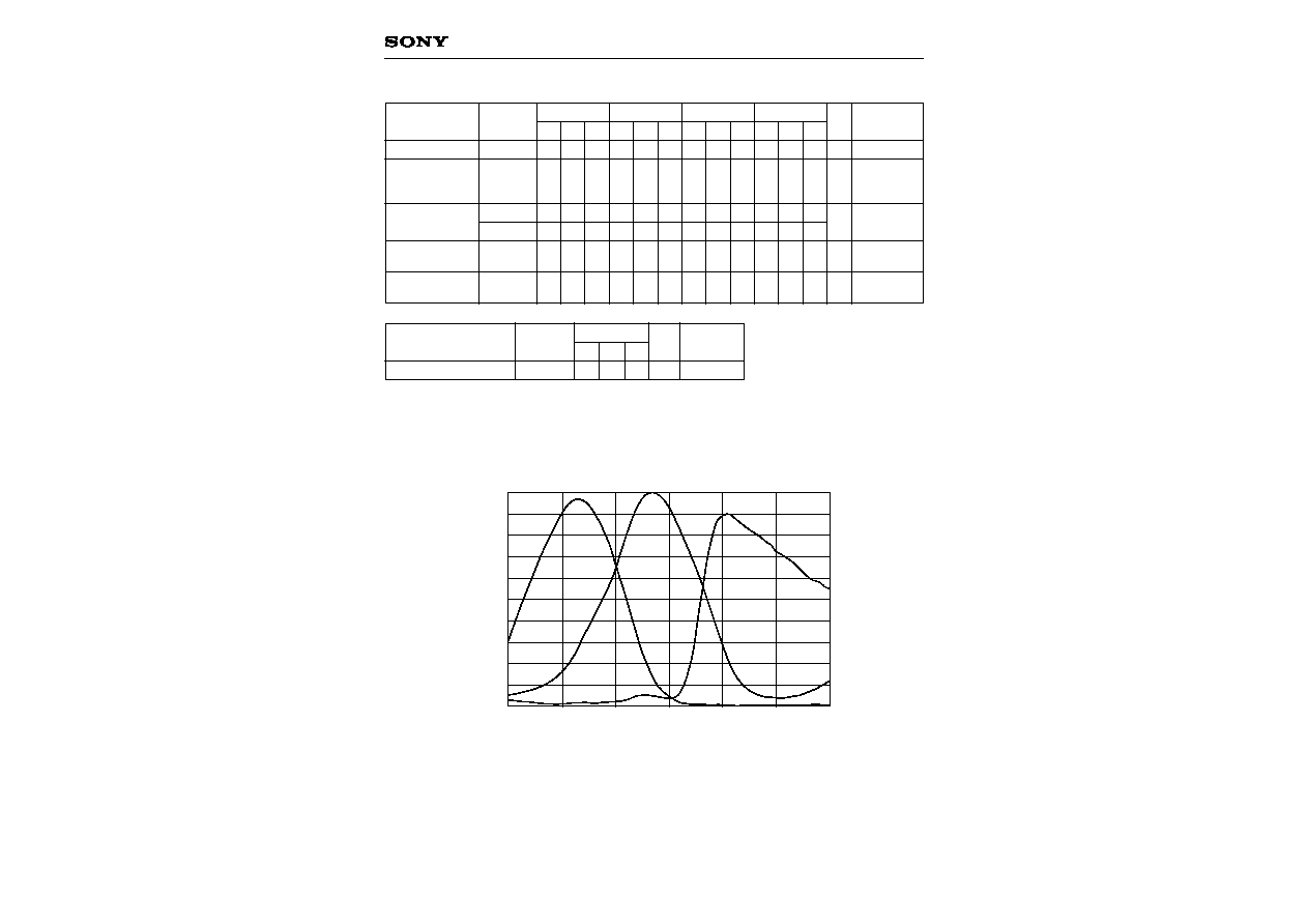
Spectral Sensitivity Characteristics (excludes lens characteristics and light source characteristics)
Clock Switching Characteristics (Horizontal drive frequency: 18MHz)
Min.
twh
Typ. Max. Min. Typ. Max. Min. Typ. Max. Min. Typ. Max.
twl
tr
tf
3.10
14
14
7
1.6
3.33
19.5
19.5
10
3.56
14
14
19.5
19.5
37
0.5
8.5
8.5
4
14
14
0.5
15
0.5
8.5
8.5
5
250
14
14
0.5
Unit
µs
ns
ns
ns
µs
Remarks
During readout
When using
CXD3400N
tf
tr ≠ 2ns
During drain
charge
Item
Readout clock
Vertical transfer
clock
Horizontal
transfer clock
Reset gate clock
Substrate clock
Symbol
V
T
V
1A
, V
1B
,
V
2
, V
3A
,
V
3B
, V
4
H
1
H
2
RG
SUB
Min.
two
Typ. Max.
12 19.5
Unit
ns
Remarks
Item
Horizontal transfer clock
Symbol
H
1
, H
2
400
1.0
B
G
R
0.9
0.8
0.7
0.6
0.5
0.4
0.3
0.2
0.1
0
450
500
550
Wave Length [nm]
Relativ
e Response
600
650
700
≠ 9 ≠
ICX406AQF
Image Sensor Characteristics (horizontal drive frequency: 18MHz)
(Ta = 25∞C)
Item
G Sensitivity
Sensitivity
comparison
Saturation signal
Smear
Video signal shading
Dark signal
Dark signal shading
Line crawl G
Line crawl R
Line crawl B
Lag
Symbol
Sg
Rr
Rb
Vsat
Sm
SHg
Vdt
Vdt
Lcg
Lcr
Lcb
Lag
Min.
180
0.35
0.40
380
Typ.
220
0.50
0.55
≠85
≠72
Max.
285
0.65
0.70
≠81.2
≠68.0
20
25
16
8
3.8
3.8
3.8
0.5
Unit
mV
mV
dB
%
mV
mV
%
%
%
%
Measurement
method
1
1
1
2
3
4
5
6
7
7
7
8
Remarks
1/30s accumulation
Ta = 60∞C
Frame readout mode
1
High frame rate readout mode
Zone 0 and
I
Zone 0 to
II
'
Ta = 60∞C, 3.33 frame/s
Ta = 60∞C, 3.33 frame/s,
2
1
After closing the mechanical shutter, the smear can be reduced to below the detection limit by performing
vertical register sweep operation.
2
Excludes vertical dark signal shading caused by vertical register high-speed transfer.
2
V
10
2
4
4
Ignored region
Effective pixel region
Zone 0,
I
Zone
II
,
II
'
V
10
H
8
H
8
2312 (H)
1720 (V)
Zone Definition of Video Signal Shading
Measurement System
CCD
C.D.S
S/H
S/H
AMP
CCD signal output [
A]
Gr/Gb channel signal output [
B]
R/B channel signal output [
C]
Note) Adjust the amplifier gain so that the gain between [
A] and [
B], and between [
A] and [
C] equals 1.
R
B
≠ 10 ≠
ICX406AQF
Image Sensor Characteristics Measurement Method
Measurement conditions
(1) In the following measurements, the device drive conditions are at the typical values of the bias and clock
voltage conditions, and the frame readout mode is used.
(2) In the following measurements, spot blemishes are excluded and, unless otherwise specified, the optical
black level (OB) is used as the reference for the signal output, which is taken as the value of the Gr/Gb
channel signal output or the R/B channnel signal output of the measurement system.
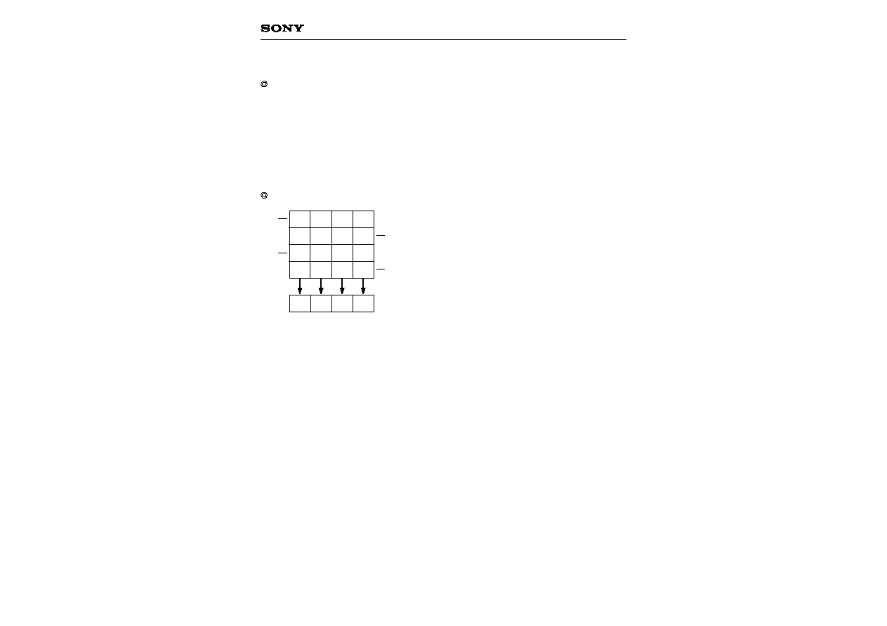
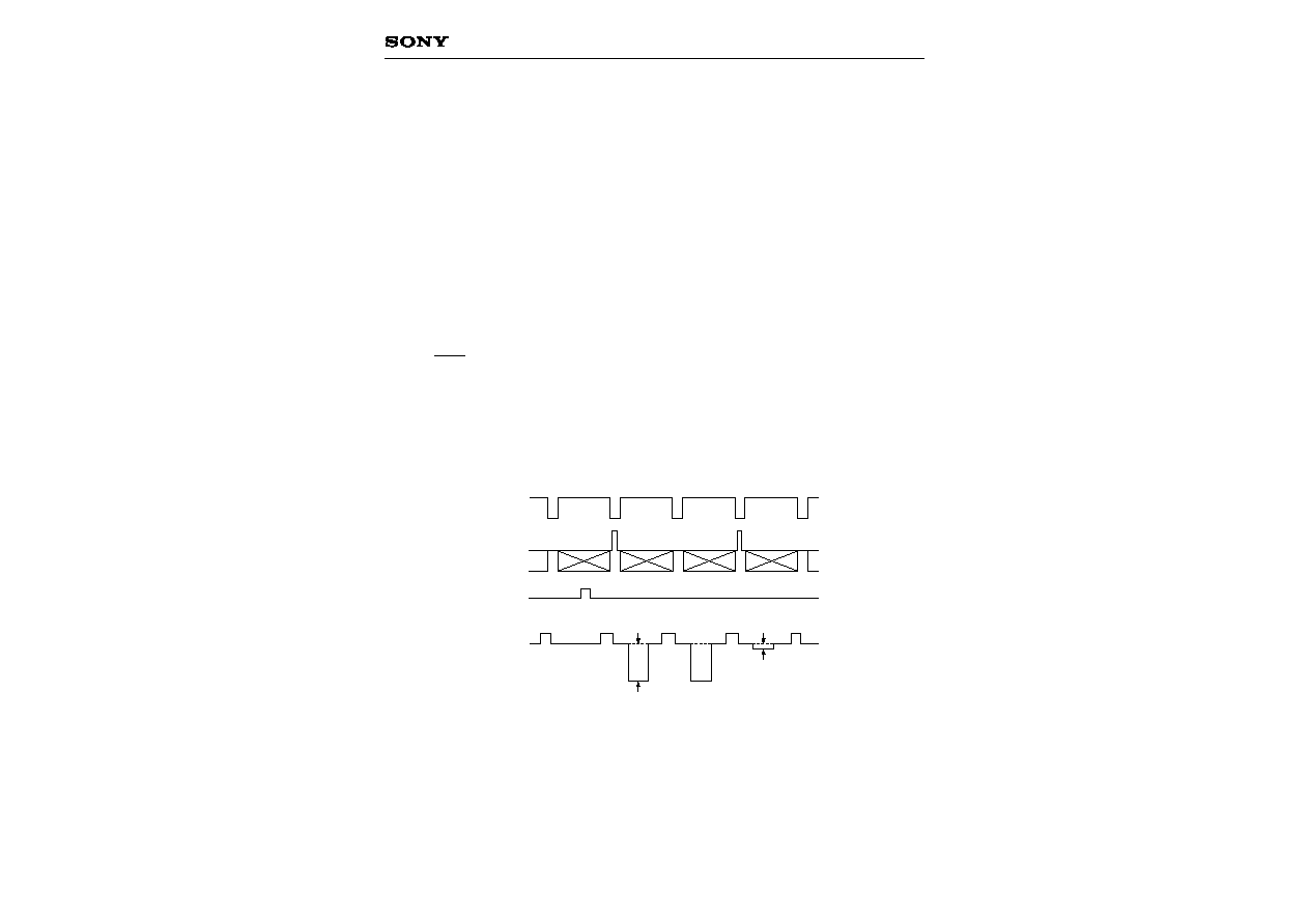
Color coding of this image sensor & Readout
The primary color filters of this image sensor are arranged in
the layout shown in the figure on the left (Bayer arrangement).
Gr and Gb denote the G signals on the same line as the R
signal and the B signal, respectively.
For frame readout, the A1 and A2 lines are output as signals in
the A field, and the B1 and B2 lines in the B field.
Gb
B
Gb
B
R
Gr
R
Gr
Gb
B
Gb
B
R
Gr
R
Gr
B2
B1
A2
A1
Horizontal register
Color Coding Diagram
≠ 11 ≠
ICX406AQF
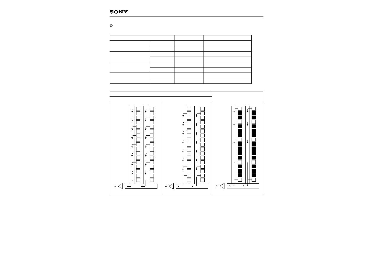
2. Frame readout mode, high frame rate readout mode
Frame readout mode
High frame rate readout mode
1st field
2nd field
17
16
15
14
13
12
11
10
9
8
7
6
5
4
3
1
2
V
OUT
R
Gb
R
Gb
R
Gb
R
Gb
R
Gb
R
Gb
R
Gb
R
R
Gb
Gr
B
Gr
B
Gr
B
Gr
B
Gr
B
Gr
B
Gr
B
Gr
Gr
B
17
16
15
14
13
12
11
10
9
8
7
6
5
4
3
1
2
V
OUT
R
Gb
R
Gb
R
Gb
R
Gb
R
Gb
R
Gb
R
Gb
R
R
Gb
Gr
B
Gr
B
Gr
B
Gr
B
Gr
B
Gr
B
Gr
B
Gr
Gr
B
17
16
15
14
13
12
11
10
9
8
7
6
5
4
3
1
2
V
OUT
R
Gb
R
Gb
R
Gb
R
Gb
R
Gb
R
Gb
R
Gb
R
R
Gb
Gr
B
Gr
B
Gr
B
Gr
B
Gr
B
Gr
B
Gr
B
Gr
Gr
B
Readout modes
1. Readout modes list
Mode name
Frame rate
Number of effective output lines
Frame readout mode
High frame rate readout
mode
AF1 mode
AF2 mode
NTSC mode
PAL mode
NTSC mode
PAL mode
NTSC mode
PAL mode
NTSC mode
PAL mode
3.33 frame/s
3.57 frame/s
30 frame/s
25 frame/s
60 frame/s
50 frame/s
120 frame/s
100 frame/s
1720 (Odd 860, Even 860)
1720 (Odd 860, Even 860)
215
215
97
119
35
46
Note) Blacked out portions in the diagram indicate pixels which are not read out.
1. Frame readout mode
In this mode, all pixel signals are divided into two fields and output.
All pixel signals are read out independently, making this mode suitable for high resolution image capturing.
2. High frame rate readout mode
Output is performed at 30 frames per second by reading out 4 pixels for every 16 vertical pixels and adding
2 pixels in the horizontal CCD.
The number of output lines is 215 lines.
This readout mode emphasizes processing speed over vertical resolution.
≠ 12 ≠
ICX406AQF
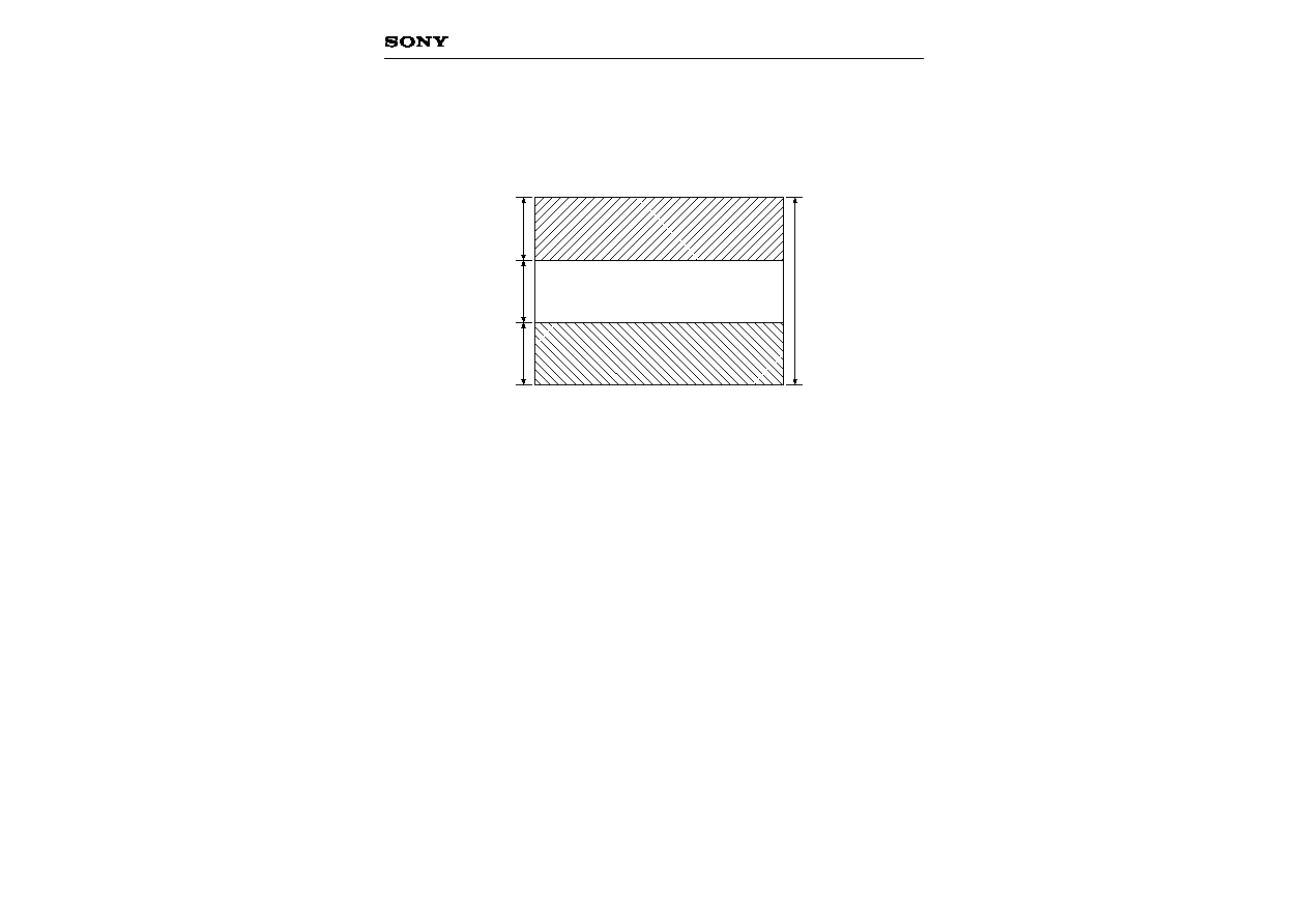
3. AF1 mode, AF2 mode
The AF modes increase the frame rate by cutting out a portion of the picture through high-speed elimination of
the top and bottom of the picture in high frame rate readout mode. AF1 allows 1/60s and 1/50s output, and AF2
allows 1/120s and 1/100s output, so these modes are effective for raising the auto focus (AF) speed.
Number of effective lines
in high frame rate
readout mode
215
Top
frame shift region
Cut-out region
Bottom
high-speed sweep region
≠ 13 ≠
ICX406AQF
Definition of standard imaging conditions
(1) Standard imaging condition
I
:
Use a pattern box (luminance: 706cd/m
2
, color temperature of 3200K halogen source) as a subject.
(Pattern for evaluation is not applicable.) Use a testing standard lens with CM500S (t = 1.0mm) as an IR
cut filter and image at F5.6. The luminous intensity to the sensor receiving surface at this point is defined
as the standard sensitivity testing luminous intensity.
(2) Standard imaging condition
II
:
Image a light source (color temperature of 3200K) with a uniformity of brightness within 2% at all angles.
Use a testing standard lens with CM500S (t = 1.0mm) as an IR cut filter. The luminous intensity is adjusted
to the value indicated in each testing item by the lens diaphragm.
(3)Standard imaging condition
III
:
Image a light source (color temperature of 3200K) with a uniformity of brightness within 2% at all angles.
Use a testing standard lens (exit pupil distance ≠33mm) with CM500S (t = 1.0mm) as an IR cut filter. The
luminous intensity is adjusted to the value indicated in each testing item by the lens diagram.
1. G Sensitivity, sensitivity comparison
Set to the standard imaging condition
I
. After setting the electronic shutter mode with a shutter speed of
1/100s, measure the signal outputs (V
Gr
, V
Gb
, V
R
and V
B
) at the center of each Gr, Gb, R and B channel
screen, and substitute the values into the following formulas.
V
G
= (V
Gr
+ V
Gb
) /2
Sg = V
G
◊
[mV]
Rr = V
R
/V
G
Rb = V
B
/V
G
2. Saturation signal
Set to the standard imaging condition
II
. After adjusting the luminous intensity to 20 times the intensity with
the average value of the Gr signal output, 150mV, measure the minimum values of the Gr, Gb, R and B
signal outputs.
3. Smear
Set to the standard imaging condition
II
. With the lens diaphragm at F5.6 to F8, first adjust the average
value of the Gr signal output to 150mV. Measure the average values of the Gr signal output, Gb signal
output, R signal output and B signal output (Gra, Gba, Ra, Ba), and then adjust the luminous intensity to
500 times the intensity with the average value of the Gr signal output, 150mV.
After the readout clock is stopped and the charge drain is executed by the electronic shutter at the
respective H blankings, measure the maximum value (Vsm [mV]) independent of the Gr, Gb, R and B
signal outputs, and substitute the values into the following formula.
Sm = 20
◊
log
(
Vsm
˜
◊
◊
)
[dB] (1/10V method conversion value)
4. Video signal shading
Set to the standard imaging condition
III
. With the lens diaphragm at F5.6 to F8, adjusting the luminous
intensity so that the average value of the Gr signal output is 150mV. Then measure the maximum value
(Grmax [mV]) and minimum value (Grmin [mV]) of the Gr signal output and substitute the values into the
following formula.
SHg = (Grmax ≠ Grmin) /150
◊
100 [%]
1
10
1
500
Gra + Gba + Ra + Ba
4
100
30
≠ 14 ≠
ICX406AQF
5. Dark signal
Measure the average value of the signal output (Vdt [mV]) with the device ambient temperature of 60∞C
and the device in the light-obstructed state, using the horizontal idle transfer level as a reference.
6. Dark signal shading
After measuring 5, measure the maximum (Vdmax [mV]) and minimum (Vdmin [mV]) values of the dark
signal output and substitute the values into the following formula.
Vdt = Vdmax ≠ Vdmin [mV]
7. Line crawl
Set to the standard imaging condition
II
. Adjusting the luminous intensity so that the average value of the
Gr signal output is 150mV, and then insert R, G and B filters and measure the difference between G signal
lines (
Glr,
Glg,
Glb [mV]) as well as the average value of the G signal output (Gar, Gag, Gab).
Substitute the values into the following formula.
Lci =
◊
100 [%] (i = r, g, b)
8. Lag
Adjust the Gr signal output value generated by the strobe light to 150mV. After setting the strobe light so
that it strobes with the following timing, measure the residual signal amount (Vlag). Substitute the value
into the following formula.
Lag = (Vlag/150)
◊
100 [%]
Light
VD
V1A/V1B
Strobe light timing
Output
Vlag (lag)
Gr signal output 150mV
Gli
Gai
≠ 15 ≠
ICX406AQF
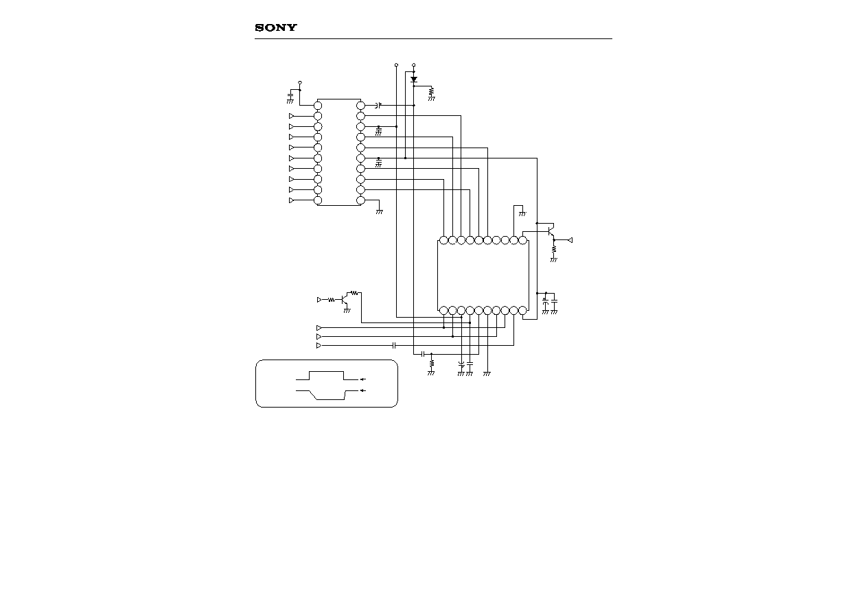
Drive Circuit
Notes) Substrate bias control
1. The saturation signal level decreases when exposure is performed using the mechanical shutter,
so control the substrate bias.
2. A saturation signal level equivalent to that for continuous exposure can be assured by connecting
a 2.7k
grounding registor to the CCD C
SUB
pin.
Drive timing precautions
1. Blooming occurs in modes (high frame rate readout, etc.) that do not use the mechanical shitter,
so do not ground the connected 2.7k
resistor.
2. tf is slow, so the internally generated voltage V
SUB
may not drop to a sufficiently low level if the
substrate bias control signal is not set to high level 10ms before entering the exposure period
and the 2.7k
resistor connected to the C
SUB
pin is not grounded.
3. The blooming signal generated during exposure in mechanical shutter mode is swept by
providing two fields or more of idle transfer through vertical register high-speed sweep transfer
from the time the mechanical shutter closes until sensor readout is performed. However, note
that the V
L
potential and the
SUB pin DC voltage sag at this time.
Substrate bias
control signal
V
SUB
Cont.
Mechanical
shutter mode
Substrate bias
SUB pin voltage
GND
tr
2ms
tf
4ms
Internally
generated
value V
SUB
XSUB
XV3
XSG3B
XSG3A
XV1
XSG1B
XSG1A
XV4
XV2
V
SUB
Cont.
H
2
H
1
RG
0.1
0.1
0.1
0.1
200k
0.1
0.01
3.3/20V
0.1
4.7k
100k
CCD OUT
2SC4250
VR1 (2.7k)
20
19
18
17
16
15
14
13
12
11
1
2
3
4
5
6
7
8
9
10
CXD3400N
1
2
3
4
5
6
7
8
9
10
20 19 18 17 16 15 14 13 12 11
ICX406
(BOTTOM VIEW)
3.3/16V
1/35V
3.3V
≠7.5V
15V
H
2
RG
GND
V
DD
H
2
H
1
V
L
C
SUB
SUB
H
1
TEST
GND
V
OUT
V
4
V
3A
V
3B
V
2
V
1A
TEST
V
1B
≠
16
≠
ICX406A
QF
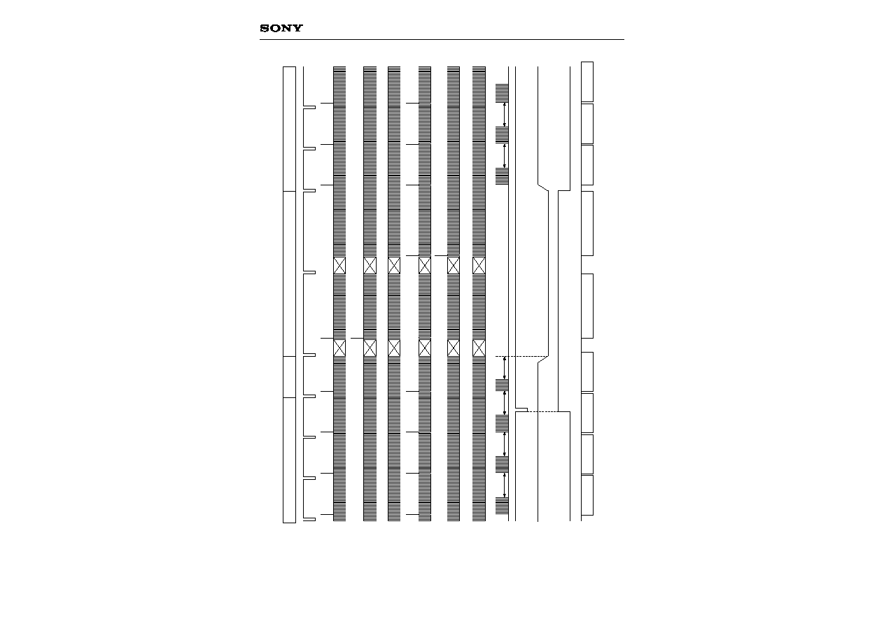
Drive Timing Chart (Vertical Sequence) High Frame Rate Readout Mode
Frame Readout Mode/Electronic Shutter Normal Operation
Note) The B output signal contain a blooming component and should therefore not be used.
Apply 20 or more electronic shutter pulses at the start of exposure for the recording image. If less than 20 pulses are applied, the electronic shutter may occur a discharge error.
VD
Act.
CCD
OUT
V1A
SUB
TRG
Mechanical
shutter
V
SUB
Cont.
OPEN
OPEN
CLOSE
V1B
V3A
V4
V2
V3B
A
B
B
D
E
C
A signal output
A signal output
B signal output B signal output
C signal output (ODD)
C signal output (EVEN)
Output after
frame readout
D signal output E signal output
High frame rate readout mode
High frame rate readout mode
Exposure operation
Frame readout mode
≠
17
≠
ICX406A
QF
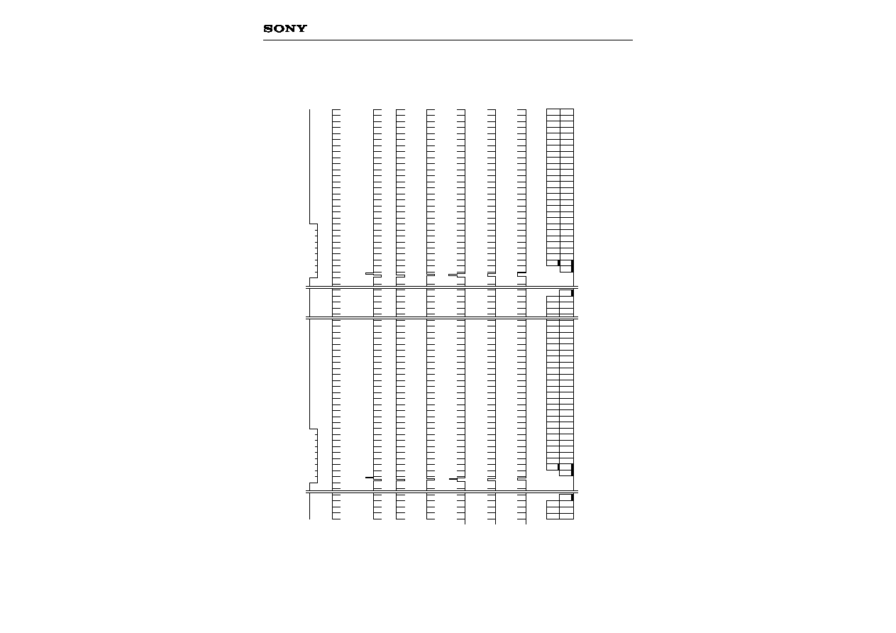
Drive Timing Chart (Vertical Sync) NTSC/PAL Frame Readout Mode
NTSC: 3.33 frame/s, PAL: 3.57 frame/s
Note) The 1013H and 2026H horizontal period in NTSC mode are 1672clk, the 945H and 1890H horizontal period in PAL mode are 464clk.
HD
Exposure period
All pixels output period
VD
1720
1718
2
4
6
8
10
12
2
4
6
8
10
1
9
3
5
7
9
11
1
3
5
7
1719
1717
CCD
OUT
V4
V3A/V3B
V1A/V1B
V2
SUB
TRG
Mechanical
shutter
V
SUB
Cont.
OPEN
OPEN
1014
2026
1
2
3
"a"
"b"
"c"
77
77
83
83
1890
1956
1888
1955
1887
1
2
3
946
1013
945
943
943
942
942
1023
955
1022
954
1088
1020
1090
1022
1096
1028
1086
1018
10
73
PAL
1
2
3
10
73
76
76
"c"
1
2
3
CLOSE
NTSC
≠
18
≠
ICX406A
QF
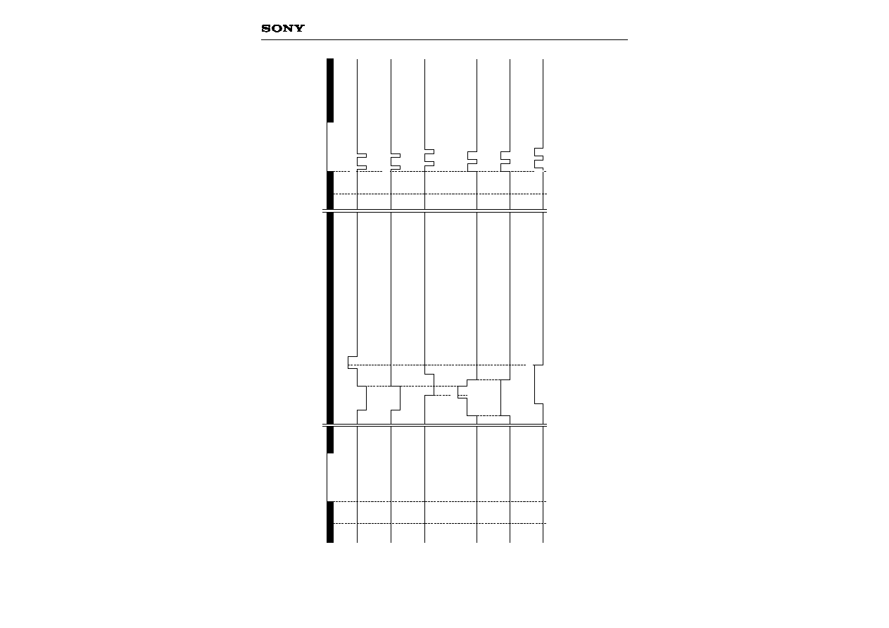
Drive Timing Chart (Readout) NTSC/PAL Frame Readout Mode
"a" Enlarged
2669
1
60
317
1104
124
156
188
252
220
284
NTSC: #1088
PAL:
#1020
NTSC: #76
PAL:
#76
NTSC: #77
PAL:
#77
1168
1200 1260
1292
1136
317
V1A/V1B
V2
V4
V2
V4
V3A/V3B
V1A/V1B
V3A/V3B
H1
2669
1
60
NTSC: #1089
PAL:
#1021
1202
"b" Enlarged
≠
19
≠
ICX406A
QF
Drive Timing Chart (High-speed Sweep Operation) NTSC/PAL Frame Readout Mode
"c" Enlarged
V1A/V1B
V2
V3A/V3B
V4
#1
#2
#3
#4
#1739
1
60
HD
28 28 28 28 28 28 28 28 28 28 28 28 28 28 28 28
28 28 28 28
194837clk = 73 lines
≠
20
≠
ICX406A
QF
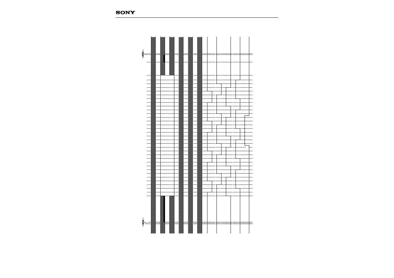
Drive Timing Chart (Horizontal Sync) NTSC/PAL Frame Readout Mode
H1
H2
RG
CLK
SHD
SUB
V2
129
1
65
96
96
32
1
1
1
1
1
1
96
160
1
1
97
1
33
1
85
160
64
1
1
108
1
64
SHP
V1A/V1B
V3A/V3B
V4
2669
Ignored pixel 2 bits
Ignored pixel 2 bits
60
1
56
1
317
345
361
257
28
1
1
16
364
1
5
3
≠
21
≠
ICX406A
QF
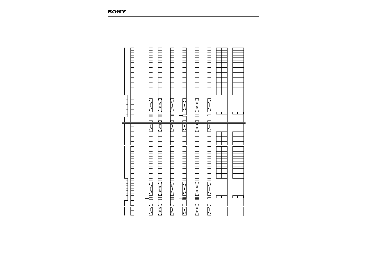
Drive Timing Chart (Vertical Sync) NTSC/PAL High Frame Rate Readout Mode
NTSC: 30 frame/s, PAL: 25 frame/s
Note) The 226H and 225H horizontal period in NTSC mode are 1372clk, the 270H in PAL mode is 2039clk.
HD
VD
1713
1706
1717
1710
5
10
21
14
37
30
53
46
69
62
85
78
94
1
6
1
17
10
33
26
49
42
65
58
81
74
90
1713
1706
1717
1710
5
10
21
14
37
30
53
46
69
62
85
78
94
1
6
1
17
10
33
26
49
42
65
58
81
74
90
CCD
OUT
V3A
V3B
V4
V2
V1A
V1B
10
10
9
9
1
1
226
270
218
218
10
PAL
"d"
"d"
218
270
1
10
9
9
218
226
1
2
3
2
3
4
4
5
5
NTSC
≠
22
≠
ICX406A
QF
Drive Timing Chart (Readout) NTSC/PAL High Frame Rate Readout Mode
"d" Enlarged
2669
1
60
317
60
60
84
#1
#2
1168
1104
1292
1356 1416
1260
1136
1202
1324
317
V1A
V1B
V2
V3B
V4
V3A
H1
2669
1
60
1200
1358
68
68
76
≠
23
≠
ICX406A
QF
Drive Timing Chart (Horizontal Sync) NTSC/PAL High Frame Rate Readout Mode, AF1 Mode, AF2 Mode
H1
H2
RG
CLK
SHD
SUB
V2
1
1
1
1
16
1
SHP
V1A/V1B
V3A/V3B
V4
2669
5
Ignored pixel 2 bits
Ignored pixel 2 bits
60
1
56
1
317
345
361
257
28
1
1
16
364
1
8
1
24
1
40
1
24
1
40
1
24
1
33
17
25
85
9
40
1
24
1
24
1
24
1
40
1
24
1
40
1
24
1
40
1
24
1
40
1
24
1
40
1
24
1
40
1
24
40
1
1
40
1
1
24
1
40
1
24
1
40
1
1
64
1
24
40
1
108
3
1
≠
24
≠
ICX406A
QF
Drive Timing Chart (Vertical Sync) NTSC/PAL AF1 Mode
NTSC: 60 frame/s, PAL: 50 frame/s
Note) The 113H horizontal period in NTSC mode is 1372clk, the 135H horizongal period in PAL mode is 2354clk.
HD
VD
CCD
OUT
465
474
481
490
469
478
485
494
465
474
481
490
469
478
485
494
10
6
1402
1406
1409
1413
10
6
PAL
465
474
481
490
469
478
485
494
465
474
481
490
469
478
485
494
10
6
1226
1230
1233
1237
10
6
NTSC
V3A
V3B
V4
V2
V1A
V1B
1
"e"
"g"
"f"
1
113
135
106
128
10
10
9
9
10
PAL
1
2
3
10
9
9
"f"
"e"
"g"
1
135
113
2
3
4
5
4
5
NTSC
≠
25
≠
ICX406A
QF
Drive Timing Chart (Vertical Sync) NTSC/PAL AF2 Mode
NTSC: 120 frame/s, PAL: 100 frame/s
Note) The 57H horizontal period in NTSC mode is 686clk, the 68H horizontal period in PAL mode is 1177clk.
HD
VD
CCD
OUT
721
730
737
746
725
734
741
750
721
730
737
746
725
734
741
750
721
730
737
746
725
734
741
750
721
730
737
746
725
734
741
750
10
6
1073
1077
1082
1086
10
6
PAL
10
6
986
990
993
997
10
6
NTSC
V3A
V3B
V4
V2
V1A
V1B
1
"e"
"i"
"h"
1
57
68
47
58
10
10
9
9
10
PAL
1
2
3
10
9
9
"h"
"e"
"i"
1
68
57
2
3
4
5
4
5
NTSC
≠
26
≠
ICX406A
QF
Drive Timing Chart (Readout) NTSC/PAL AF1 Mode, AF2 Mode
2669
1
60
317
60
60
84
1168
1104
1292
1488 1552
1496 1560
1480 1544
1356 1416
1260
1456 1520
1136
1202
1324
1472 1536
317
V1A
V1B
V2
V3B
V4
V3A
H1
2669
1
60
1200
1358
1504 1568
1464 1528
1448 1512
68
68
76
"e" Enlarged

≠
27
≠
ICX406A
QF
Drive Timing Chart NTSC/PAL AF1 Mode
"f" Enlarged
V1A/V1B
V2
V3A/V3B
V4
#2
#3
#4
#228
1
60
HD
8 8 8 8 8 8 8 8
16014clk = 6 lines
#1
≠
28
≠
ICX406A
QF
Drive Timing Chart NTSC/PAL AF1 Mode
"g" Enlarged
V1A/V1B
V2
V3A/V3B
V4
#2
#3
#4
#244
1
60
HD
8 8 8 8 8 8 8 8
16014clk = 6 lines
#1
NTSC: 107H
PAL:
129H
NTSC: 113H
PAL:
135H
NTSC: 1H
PAL:
1H
≠
29
≠
ICX406A
QF
Drive Timing Chart NTSC/PAL AF2 Mode
"h" Enlarged
V1A/V1B
V2
V3A/V3B
V4
#2
#3
#4
#356
1
60
HD
8 8 8 8 8 8 8 8
24021clk = 9 lines
#1
≠
30
≠
ICX406A
QF
Drive Timing Chart NTSC/PAL AF2 Mode
"i" Enlarged
V1A/V1B
V2
V3A/V3B
V4
#2
#3
#4
#364
1
60
HD
8 8 8 8 8 8 8 8
24021clk = 9 lines
#1
NTSC: 48H
PAL:
59H
NTSC: 57H
PAL:
68H
NTSC: 1H
PAL:
1H
≠ 31 ≠
ICX406AQF
Notes on Handling
1) Static charge prevention
CCD image sensors are easily damaged by static discharge. Before handling be sure to take the following
protective measures.
a) Either handle bare handed or use non-chargeable gloves, clothes or material.
Also use conductive shoes.
b) When handling directly use an earth band.
c) Install a conductive mat on the floor or working table to prevent the generation of static electricity.
d) Ionized air is recommended for discharge when handling CCD image sensors.
e) For the shipment of mounted substrates, use boxes treated for the prevention of static charges.
2) Soldering
a) Make sure the package temperature does not exceed 80∞C.
b) Solder dipping in a mounting furnace causes damage to the glass and other defects. Use a ground 30W
soldering iron and solder each pin in less than 2 seconds. For repairs and remount, cool sufficiently.
c) To dismount an image sensor, do not use a solder suction equipment. When using an electric desoldering
tool, use a thermal controller of the zero-cross On/Off type and connect it to ground.
3) Dust and dirt protection
Image sensors are packed and delivered by taking care of protecting its glass plates from harmful dust and
dirt. Clean glass plates with the following operations as required, and use them.
a) Perform all assembly operations in a clean room (class 1000 or less).
b) Do not either touch glass plates by hand or have any object come in contact with glass surfaces. Should
dirt stick to a glass surface, blow it off with an air blower. (For dirt stuck through static electricity ionized
air is recommended.)
c) Clean with a cotton bud and ethyl alcohol if grease stained. Be careful not to scratch the glass.
d) Keep in a case to protect from dust and dirt. To prevent dew condensation, preheat or precool when
moving to a room with great temperature differences.
e) When a protective tape is applied before shipping, just before use remove the tape applied for electrostatic
protection. Do not reuse the tape.
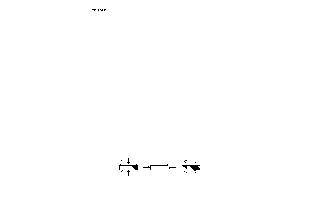
4) Installing (attaching)
a) Remain within the following limits when applying a static load to the package. Do not apply any load
more than 0.7mm inside the outer perimeter of the glass portion, and do not apply any load or impact to
limited portions. (This may cause cracks in the package.)
Plastic package
Cover glass
Compressive strength
50N
50N
1.2Nm
Torsional strength
b) If a load is applied to the entire surface by a hard component, bending stress may be generated and the
package may fracture, etc., depending on the flatness of the bottom of the package. Therefore, for
installation, use either an elastic load, such as a spring plate, or an adhesive.
≠ 32 ≠
ICX406AQF
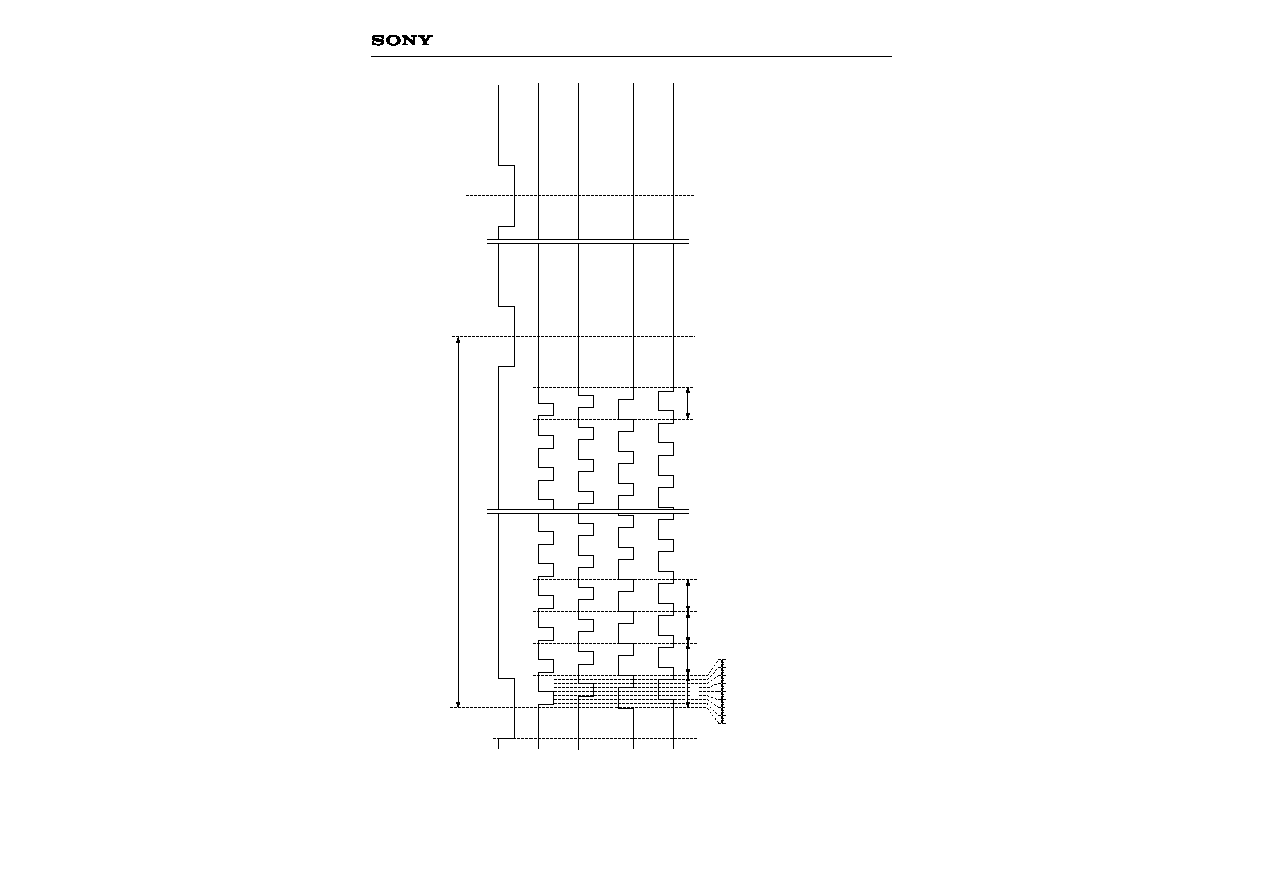
The cross section of lead frame can be seen on the side of the package for structure A.
Structure A
Structure B
Chip
Metal plate
(lead frame)
Package
Cross section of
lead frame
c) The adhesive may cause the marking on the rear surface to disappear, especially in case the regulated
voltage value is indicated on the rear surface. Therefore, the adhesive should not be applied to this area,
and indicated values should be transferred to other locations as a precaution.
d) The notch of the package is used for directional index, and that can not be used for reference of fixing.
In addition, the cover glass and seal resin may overlap with the notch of the package.
e) If the leads are bent repeatedly and metal, etc., clash or rub against the package, the dust may be
generated by the fragments of resin.
f) Acrylate anaerobic adhesives are generally used to attach CCD image sensors. In addition, cyano-
acrylate instantaneous adhesives are sometimes used jointly with acrylate anaerobic adhesives.
(reference)
5) Others
a) Do not expose to strong light (sun rays) for long periods, as color filters will be discolored. When high
luminous objects are imaged with the exposure level controlled by the electronic iris, the luminance of
the image-plane may become excessive and discoloring of the color filter will possibly be accelerated.
In such a case, it is advisable that taking-lens with the automatic-iris and closing of the shutter during
the power-off mode should be properly arranged. For continuous using under cruel condition exceeding
the normal using condition, consult our company.
b) Exposure to high temperature or humidity will affect the characteristics. Accordingly avoid storage or
usage in such conditions.
c) Brown stains may be seen on the bottom or side of the package. But this does not affect the CCD
characteristics.
d) This package has 2 kinds of internal structure. However, their package outline, optical size, and strength
are the same.
≠
33
≠
ICX406A
QF
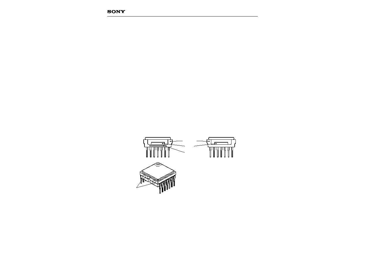
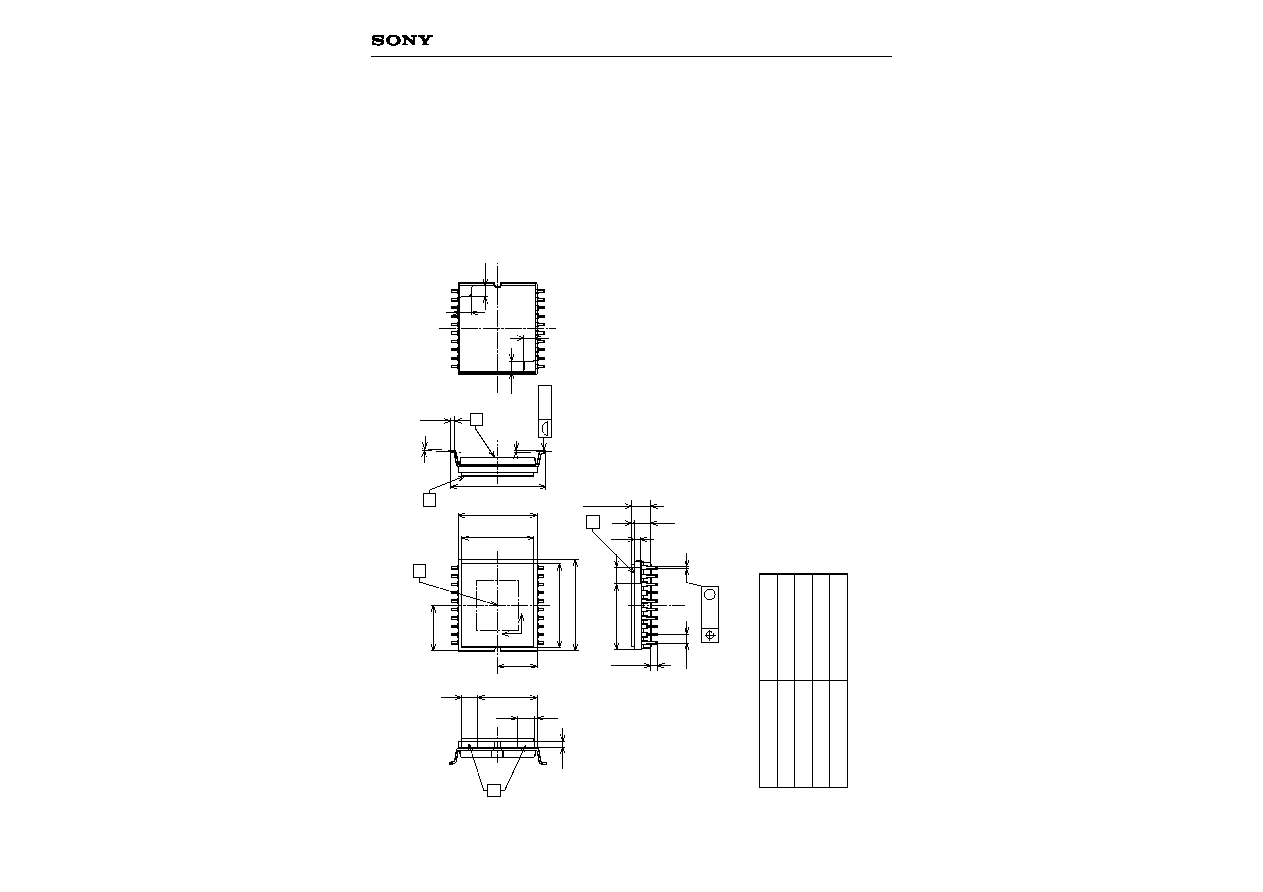
Package Outline Unit: mm
Son
y Cor
por
ation
PACKAGE STRUCTURE
PACKAGE MATERIAL
LEAD TREATMENT
LEAD MATERIAL
PACKAGE MASS
DRAWING NUMBER
20 pin SOP
Plastic
GOLD PLATING
42 ALLOY
AS-B7-03(E)
0.95g
B
0.5
2.5
9.0
2.5
0.8
A
1
10
11
20
1
10
11
C
B'
20
H
V
D
0.3
1.27
10.0
2.5
1.7
0.8
2.4
0.5
10.9
12.7
6.0
6.9
1.7
1.7
14.0 ± 0.15
(0.6)
1.7
1.0 ± 0.1
M
~
~
~
13.8 ± 0.1
12.0 ± 0.1
2.9 ± 0.15
0∞ to 10∞
0.25
0.15
0.3
1. "A" is the center of the effective image area.
2. The two points "B" of the package are the horizontal reference.
The point "B'" of the package is the vertical reference.
3. The bottom "C" of the package, and the top of the cover glass "D" are the height reference.
4. The center of the effective image area relative to "B" and "B'" is (H, V) = (6.9, 6.0) ± 0.075mm.
5. The rotation angle of the effective image area relative to H and V is ±0.7∞.
6. The height from the bottom "C" to the effective image area is 1.41 ± 0.10mm.
The height from the top of the cover glass "D" to the effective image area is 1.49 ± 0.15mm.
7. The tilt of the effective image area relative to the bottom "C" is less than 50µm.
The tilt of the effective image area relative to the top "D" of the cover glass is less than 50µm.
8. The thickness of the cover glass is 0.5mm, and the refractive index is 1.5.
9. The notches on the bottom of the package are used only for directional index, they must
not be used for reference of fixing.