
≠ 1 ≠
E01657-PS
Sony reserves the right to change products and specifications without prior notice. This information does not convey any license by
any implication or otherwise under any patents or other right. Application circuits shown, if any, are typical examples illustrating the
operation of the devices. Sony cannot assume responsibility for any problems arising out of the use of these circuits.
ICX412AQF
20 pin SOP (Plastic)
Description
The ICX412AQF is a diagonal 8.933mm (Type 1/1.8)
interline CCD solid-state image sensor with a square
pixel array and 3.24M effective pixels. Sensitivity,
saturation signal, smear and frame rate have been
improved compared to the ICX252AQF.
This chip features an electronic shutter with variable
charge-storage time.
R, G, B primary color mosaic filters are used as the
color filters, and at the same time high sensitivity and
low dark current are achieved through the adoption
of Super HAD CCD technology.
This chip is suitable for applications such as
electronic still cameras, etc.
Features
∑ Supports frame readout
∑ High horizontal and vertical resolution
∑ Supports high frame rate readout mode: 30 frames/s,
AF1 mode: 60 frames/s, 50 frames/s,
AF2 mode: 120 frames/s, 100 frames/s
∑ Square pixel
∑ Horizontal drive frequency: 22.5MHz
∑ No voltage adjustments (reset gate and substrate bias are not adjusted.)
∑ R, G, B primary color mosaic filters on chip
∑ High sensitivity, low dark current
∑ Continuous variable-speed shutter
∑ Excellent anti-blooming characteristics
∑ Exit pupil distance recommended range ≠20 to ≠100mm
∑ 20-pin high-precision plastic package
Device Structure
∑ Interline CCD image sensor
∑ Total number of pixels:
2140 (H)
◊
1560 (V) approx. 3.34M pixels
∑ Number of effective pixels:
2088 (H)
◊
1550 (V) approx. 3.24M pixels
∑ Number of active pixels:
2080 (H)
◊
1542 (V) approx. 3.21M pixels diagonal 8.933mm
∑ Number of recommended recording pixels:
2048 (H)
◊
1536 (V) approx. 3.15M pixels diagonal 8.832mm aspect ratio 4:3
∑ Chip size:
8.10mm (H)
◊
6.64mm (V)
∑ Unit cell size:
3.45µm (H)
◊
3.45µm (V)
∑ Optical black:
Horizontal (H) direction:
Front 4 pixels, rear 48 pixels
Vertical (V) direction:
Front 8 pixels, rear 2 pixels
∑ Number of dummy bits:
Horizontal 28
Vertical 1 (even fields only)
∑ Substrate material:
Silicon
2
8
V
H
Pin 1
Pin 11
48
4
Diagonal 8.933mm (Type 1/1.8) Frame Readout CCD Image Sensor with a Square Pixel for Color Cameras
Optical black position
(Top View)
Super HAD CCD is a trademark of Sony Corporation. The Super HAD CCD is a version of Sony's high performance CCD HAD (Hole-
Accumulation Diode) sensor with sharply improved sensitivity by the incorporation of a new semiconductor technology developed by
Sony Corporation.

≠ 2 ≠
ICX412AQF
11
12
13
14
15
16
17
18
19
20
Note)
Note) : Photo sensor
Horizontal register
V
e
r
tical register
V
DD
RG
H
2
H
1
GND
SUB
C
SUB
V
L
H
1
H
2
10
9
8
7
6
5
4
3
2
1
V
OUT
GND
TEST
TEST
V
1B
V
1A
V
2
V
3B
V
3A
V
4
B
Gr
B
Gr
B
Gb
R
Gb
R
Gb
B
Gr
B
Gr
B
Gb
R
Gb
R
Gb
Gr
R
Gr
R
Block Diagram and Pin Configuration
(Top View)
Pin Description
Pin No.
Description
Pin No.
Symbol
Description
1
2
3
4
5
6
7
8
9
10
V
4
V
3A
V
3B
V
2
V
1A
V
1B
TEST
TEST
GND
V
OUT
Vertical register transfer clock
Vertical register transfer clock
Vertical register transfer clock
Vertical register transfer clock
Vertical register transfer clock
Vertical register transfer clock
Test pin
1
Test pin
1
GND
Signal output
11
12
13
14
15
16
17
18
19
20
V
DD
RG
H
2
H
1
GND
SUB
C
SUB
V
L
H
1
H
2
1
Leave this pin open
2
DC bias is generated within the CCD, so that this pin should be grounded externally through a capacitance
of 0.1µF.
Supply voltage
Reset gate clock
Horizontal register transfer clock
Horizontal register transfer clock
GND
Substrate clock
Substrate bias
2
Protective transistor bias
Horizontal register transfer clock
Horizontal register transfer clock
Symbol
≠ 4 ≠
ICX412AQF
Bias Conditions
Supply voltage
Protective transistor bias
Substrate clock
Reset gate clock
Item
V
DD
V
L
SUB
RG
Symbol
15.0
1
2
2
Min.
V
Unit
Remarks
Typ.
Max.
1
V
L
setting is the V
VL
voltage of the vertical clock waveform, or the same voltage as the V
L
power supply for
the V driver should be used.
2
Do not apply a DC bias to the substrate clock and reset gate clock pins, because a DC bias is generated
within the CCD.
DC Characteristics
14.55
15.45
Supply current
Item
I
DD
Symbol
7.5
Min.
Unit
Remarks
Typ.
Max.
mA
9.5
5.5
Clock Voltage Conditions
Readout clock voltage
Vertical transfer clock
voltage
Horizontal transfer
clock voltage
Reset gate clock
voltage
Substrate clock voltage
Item
V
VT
V
VH1
, V
VH2
V
VH3
, V
VH4
V
VL1
, V
VL2
,
V
VL3
, V
VL4
V
V
V
VH3
≠ V
VH
V
VH4
≠ V
VH
V
VHH
V
VHL
V
VLH
V
VLL
V
H
V
HL
V
CR
V
RG
V
RGLH
≠ V
RGLL
V
RGL
≠ V
RGLm
V
SUB
Symbol
14.55
≠0.05
≠0.2
≠8.0
6.8
≠0.25
≠0.25
4.0
≠0.05
0.8
3.0
21.5
Min.
15.0
0
0
≠7.5
7.5
5.0
0
2.5
3.3
22.5
Typ.
15.45
0.05
0.05
≠7.0
8.05
0.1
0.1
0.8
0.9
0.9
0.8
5.25
0.05
5.25
0.4
0.5
23.5
Max.
Unit
1
2
2
2
2
2
2
2
2
2
2
3
3
3
4
4
4
5
Waveform
Diagram
V
VH
= (V
VH1
+ V
VH2
)/2
V
VL
= (V
VL3
+ V
VL4
)/2
V
V
= V
VH
n ≠ V
VL
n (n = 1 to 4)
High-level coupling
High-level coupling
Low-level coupling
Low-level coupling
Cross-point voltage
Low-level coupling
Low-level coupling
Remarks
V
V
V
V
V
V
V
V
V
V
V
V
V
V
V
V
V
V
≠ 5 ≠
ICX412AQF
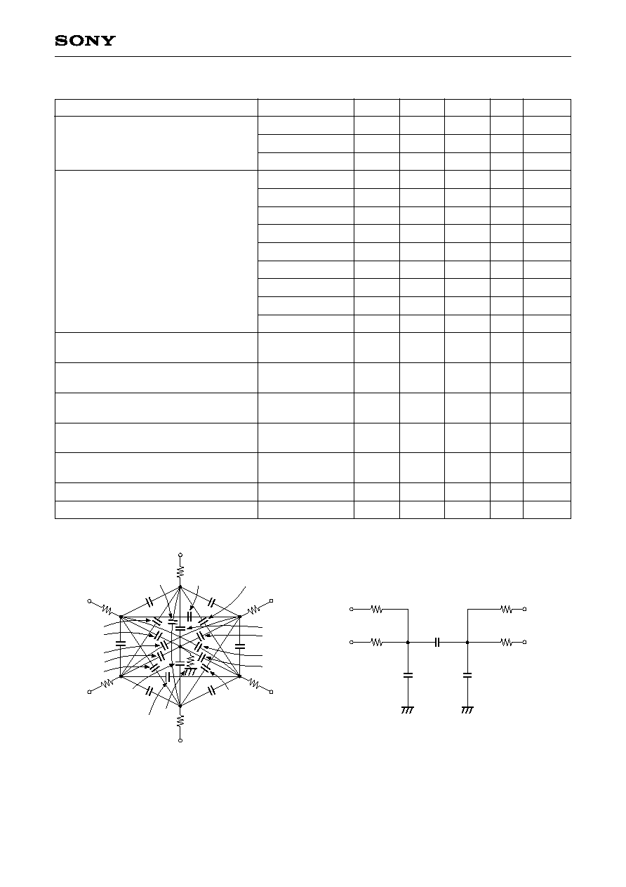
Clock Equivalent Circuit Constants
Vertical transfer clock equivalent circuit
Horizontal transfer clock equivalent circuit
H
1
H
2
C
H1
C
H2
C
HH
R
H
R
H
H
1
H
2
R
H
R
H
R
GND
C
V1B3B
R
1B
C
V41B
V
1B
C
V4
C
V41A
C
V1B
C
V1B3A
C
V1A1B
C
V1A
C
V1B2
R
1A
V
1A
C
V1A2
V
2
R
2
C
V24
C
V1A3A
C
V23A
C
V23B
R
3A
V
3A
C
V2
C
V3A
C
V3A3B
C
V1A3B
C
V3B
R
3B
V
3B
C
V3A4
C
V3B4
V
4
R
4
C
V1A
, C
V3A
C
V1B
, C
V3B
C
V2
, C
V4
C
V1A2
, C
V3A4
C
V1B2
, C
V3B4
C
V23A
, C
V41A
C
V23B
, C
V41B
C
V1A3A
C
V1B3B
C
V1A3B
, C
V1B3A
C
V24
C
V1A1B
, C
V3A3B
C
H1
, C
H2
C
HH
C
RG
C
SUB
R
1A
, R
1B
, R
2
,
R
3A
, R
3B
, R
4
R
GND
R
H
Symbol
Capacitance between vertical transfer
clock and GND
Capacitance between vertical transfer
clocks
Capacitance between horizontal transfer
clock and GND
Capacitance between horizontal transfer
clocks
Capacitance between reset gate clock
and GND
Capacitance between substrate clock
and GND
Vertical transfer clock series resistor
Vertical transfer clock ground resistor
Horizontal transfer clock series resistor
Item
Min.
Typ.
Max.
pF
pF
pF
pF
pF
pF
pF
pF
pF
pF
pF
pF
pF
pF
pF
pF
Unit
Remarks
1500
5600
2700
390
470
120
180
39
220
62
75
68
36.5
88.5
8
1000
62
18
15
