 | –≠–ª–µ–∫—Ç—Ä–æ–Ω–Ω—ã–π –∫–æ–º–ø–æ–Ω–µ–Ω—Ç: ICX432DQF | –°–∫–∞—á–∞—Ç—å:  PDF PDF  ZIP ZIP |
≠ 1 ≠
E02123A27
Sony reserves the right to change products and specifications without prior notice. This information does not convey any license by
any implication or otherwise under any patents or other right. Application circuits shown, if any, are typical examples illustrating the
operation of the devices. Sony cannot assume responsibility for any problems arising out of the use of these circuits.
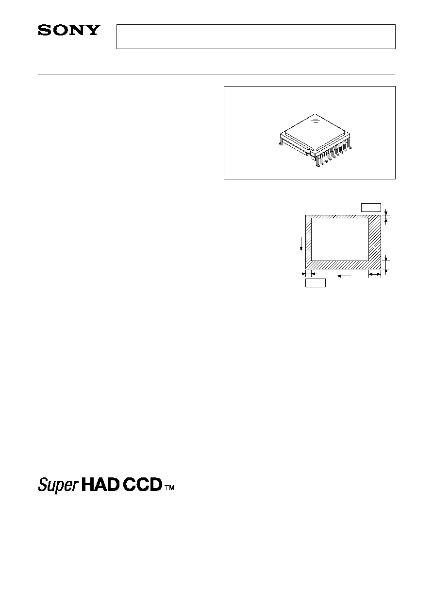
ICX432DQF
18 pin SOP (Plastic)
Diagonal 6.67mm (Type 1/2.7) Frame Readout CCD Image Sensor with a Square Pixel for Color Cameras
Optical black position
(Top View)
Super HAD CCD is a trademark of Sony Corporation. The Super HAD CCD is a version of Sony's high performance CCD HAD (Hole-
Accumulation Diode) sensor with sharply improved sensitivity by the incorporation of a new semiconductor technology developed by
Sony Corporation.
Description
The ICX432DQF is a diagonal 6.67mm (Type 1/2.7)
interline CCD solid-state image sensor with a square
pixel array and 3.24M effective pixels. Adoption of a
3-field readout system ensures small size and high
performance. This chip features an electronic shutter
with variable charge-storage time.
R, G, B primary color mosaic filters are used as
the color filters, and at the same time high sensitivity
and low dark current are achieved through the
adoption of Super HAD CCD technology.
This chip is suitable for applications such as
electronic still cameras, etc.
Features
∑ Supports frame readout system
∑ High horizontal and vertical resolution
∑ Supports high frame rate readout mode : 30 frames/s,
AF mode : 60 frames/s, 50 frames/s
∑ Square pixel
∑ Horizontal drive frequency: 24.3MHz
∑ No voltage adjustments (reset gate and substrate bias are not adjusted.)
∑ R, G, B primary color mosaic filters on chip
∑ High sensitivity, low dark current
∑ Continuous variable-speed shutter
∑ Excellent anti-blooming characteristics
∑ 18-pin high-precision plastic package
Device Structure
∑ Interline CCD image sensor
∑ Total number of pixels:
2140 (H)
◊
1560 (V) approx. 3.34M pixels
∑ Number of effective pixels: 2088 (H)
◊
1550 (V) approx. 3.24M pixels
∑ Number of active pixels:
2080 (H)
◊
1542 (V) approx. 3.21M pixels diagonal 6.667mm
∑ Number of recommended recording pixels:
2048 (H)
◊
1536 (V) approx. 3.15M pixels diagonal 6.592mm aspect ratio 4:3
∑ Chip size:
6.10mm (H)
◊
4.95mm (V)
∑ Unit cell size:
2.575µm (H)
◊
2.575µm (V)
∑ Optical black:
Horizontal (H) direction: Front 4 pixels, rear 48 pixels
Vertical (V) direction:
Front 8 pixels, rear 2 pixels
∑ Number of dummy bits:
Horizontal 28
Vertical 1 (3rd field only)
∑ Substrate material:
Silicon
2
8
V
H
Pin 1
Pin 11
48
4
≠ 2 ≠
ICX432DQF
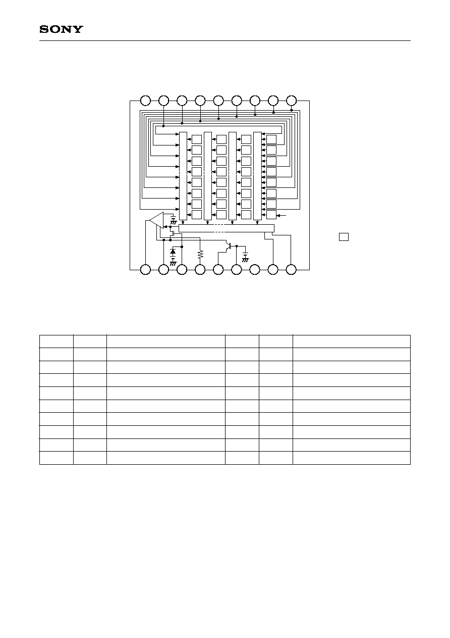
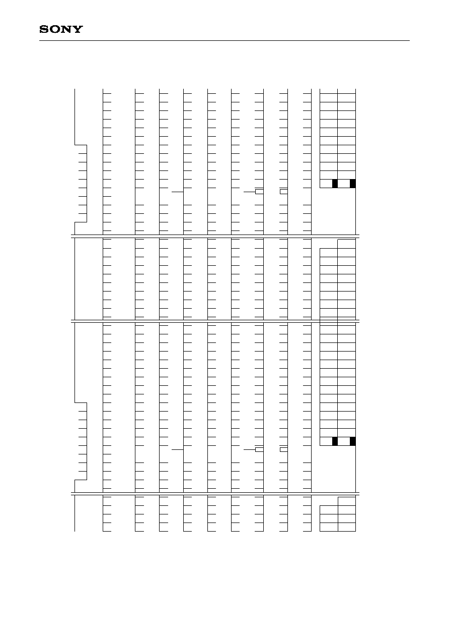
Block Diagram and Pin Configuration
(Top View)
Pin Description
Pin No.
Description
Pin No.
Symbol
Description
1
2
3
4
5
6
7
8
9
V
6
V
5B
V
5A
V
4
V
3B
V
3A
V
2
V
1
GND
Vertical register transfer clock
Vertical register transfer clock
Vertical register transfer clock
Vertical register transfer clock
Vertical register transfer clock
Vertical register transfer clock
Vertical register transfer clock
Vertical register transfer clock
GND
10
11
12
13
14
15
16
17
18
V
OUT
V
DD
RG
GND
SUB
C
SUB
V
L
H
1
H
2
1
DC bias is generated within the CCD, so that this pin should be grounded externally through a
capacitance of 0.1µF.
Signal output
Supply voltage
Reset gate clock
GND
Substrate clock
Substrate bias
1
Protective transistor bias
Horizontal register transfer clock
Horizontal register transfer clock
Symbol
10
11
12
13
14
15
16
17
18
Note)
Note) : Photo sensor
Horizontal register
V
e
r
tical register
V
OUT
V
DD
RG
GND
SUB
C
SUB
V
L
H
1
H
2
9
8
7
6
5
4
3
2
1
GND
V
1
V
2
V
3A
V
3B
V
4
V
5A
V
5B
V
6
B
Gr
B
Gr
B
Gb
R
Gb
R
Gb
B
Gr
B
Gr
B
Gb
R
Gb
R
Gb
Gr
R
Gr
R
B
Gr
Gb
R
B
Gr
Gb
R
≠ 3 ≠
ICX432DQF
Absolute Maximum Ratings
Item
V
DD
, V
OUT
,
RG ≠
SUB
V
1
, V
3A
, V
3B
, V
5A
, V
5B
≠
SUB
V
2
, V
4
, V
6
, V
L
≠
SUB
H
1
, H
2
, GND ≠
SUB
C
SUB
≠
SUB
V
DD
, V
OUT
,
RG, C
SUB
≠ GND
V
1
, V
2
, V
3A
, V
3B
, V
4
, V
5A
, V
5B
, V
6
≠ GND
H
1
, H
2
≠ GND
V
1
, V
3A
, V
3B
, V
5A
, V
5B
≠ V
L
V
2
, V
4
, V
6
, H
1
, H
2
, GND ≠ V
L
Voltage difference between vertical clock input pins
H
1
≠ H
2
H
1
, H
2
≠ V
6
Against
SUB
Against
GND
Against
V
L
Between input
clock pins
Storage temperature
Guaranteed temperature of performance
Operating temperature
≠40 to +12
≠50 to +15
≠50 to +0.3
≠40 to +0.3
≠25 to
≠0.3 to +22
≠10 to +18
≠10 to +6.5
≠0.3 to +28
≠0.3 to +15
to +15
≠6.5 to +6.5
≠10 to +16
≠30 to +80
≠10 to +60
≠10 to +75
V
V
V
V
V
V
V
V
V
V
V
V
V
∞C
∞C
∞C
1
Ratings
Unit
Remarks
1
+24V (Max.) when clock width < 10µs, clock duty factor < 0.1%.
+16V (Max.) is guaranteed for turning on or off power supply.
≠ 4 ≠
ICX432DQF
Bias Conditions
Supply voltage
Protective transistor bias
Substrate clock
Reset gate clock
Item
V
DD
V
L
SUB
RG
Symbol
15.0
1
2
2
Min.
V
Unit
Remarks
Typ.
Max.
1
V
L
setting is the V
VL
voltage of the vertical clock waveform, or the same voltage as the V
L
power supply for
the V driver should be used.
2
Do not apply a DC bias to the substrate clock and reset gate clock pins, because a DC bias is generated
within the CCD.
DC Characteristics
14.55
15.45
Supply current
Item
I
DD
Symbol
7.0
Min.
Unit
Remarks
Typ.
Max.
mA
9.0
5.0
Clock Voltage Conditions
Readout clock voltage
Vertical transfer clock
voltage
Horizontal transfer
clock voltage
Reset gate clock
voltage
Substrate clock voltage
Item
V
VT
V
VH1
, V
VH2
V
VH3
, V
VH4
V
VH5
, V
VH6
V
VL1
, V
VL2
,
V
VL3
, V
VL4
,
V
VL5
, V
VL6
V
V
V
VH5
≠ V
VH
V
VH6
≠ V
VH
V
VHH
V
VHL
V
VLH
V
VLL
V
H
V
HL
V
CR
V
RG
V
RGLH
≠ V
RGLL
V
RGL
≠ V
RGLm
V
SUB
Symbol
14.55
≠0.05
≠0.2
≠8.0
6.8
≠0.25
≠0.25
3.0
≠0.05
0.5
3.0
21.5
Min.
15.0
0
0
≠7.5
7.5
3.3
0
1.65
3.3
22.5
Typ.
15.45
0.05
0.05
≠7.0
8.05
0.1
0.1
0.8
0.9
0.9
0.8
3.6
0.05
3.6
0.4
0.5
23.5
Max.
Unit
1
2
2
2
2
2
2
2
2
2
2
3
3
3
4
4
4
5
Waveform
Diagram
V
VH
= (V
VH1
+ V
VH2
+ V
VH3
+ V
VH4
)/2
V
VL
= (V
VL5
+ V
VL6
)/2
V
V
= V
VH
n ≠ V
VL
n (n = 1 to 6)
High-level coupling
High-level coupling
Low-level coupling
Low-level coupling
Cross-point voltage
Low-level coupling
Low-level coupling
Remarks
V
V
V
V
V
V
V
V
V
V
V
V
V
V
V
V
V
V
≠ 5 ≠
ICX432DQF
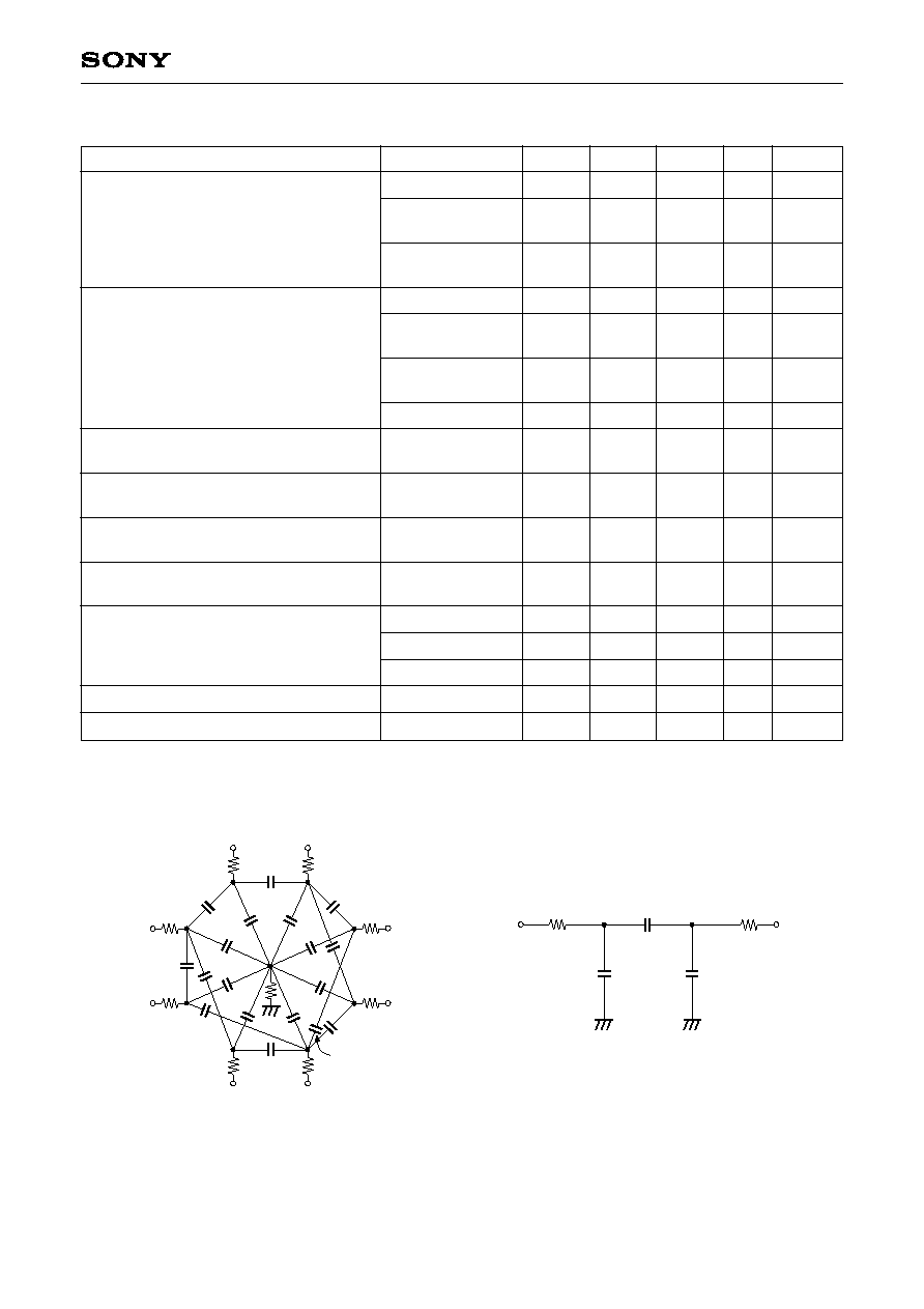
Clock Equivalent Circuit Constants
Vertical transfer clock equivalent circuit
Horizontal transfer clock equivalent circuit
C
V1
C
V3A
, C
V3B
,
C
V5A
, C
V5B
C
V2
, C
V4
,
C
V6
C
V12
C
V23A
, C
V23B
,
C
V45A
, C
V45B
C
V3A4
, C
V3B4
,
C
V5A6
, C
V5B6
C
V61
C
H1
, C
H2
C
HH
C
RG
C
SUB
R
1
, R
2
, R
4
, R
6
R
3A
, R
5A
R
3B
, R
5B
R
GND
R
H
Symbol
Capacitance between vertical transfer
clock and GND
Capacitance between vertical transfer
clocks
Capacitance between horizontal transfer
clock and GND
Capacitance between horizontal transfer
clocks
Capacitance between reset gate clock
and GND
Capacitance between substrate clock
and GND
Vertical transfer clock series resistor
Vertical transfer clock ground resistor
Horizontal transfer clock series resistor
Item
Min.
Typ.
Max.
pF
pF
pF
pF
pF
pF
pF
pF
pF
pF
pF
Unit
Remarks
1280
640
400
510
50
260
100
40
70
8
1000
60
240
80
18
13
R
GND
V
2
R
2
C
V12
V
1
V
6
V
3A
V
3B
V
4
V
5A
V
5B
R
1
R
6
R
5B
R
3A
R
3B
R
4
R
5A
C
V5B6
C
V23A
C
V3B4
C
V45A
C
V61
C
V3B
C
V23B
C
V3A
C
V3A4
C
V2
C
V1
C
V6
C
V5A6
C
V5B
C
V5A
C
V4
C
V45B
H
1
H
2
C
H1
C
H2
C
HH
R
H
R
H
≠ 6 ≠
ICX432DQF
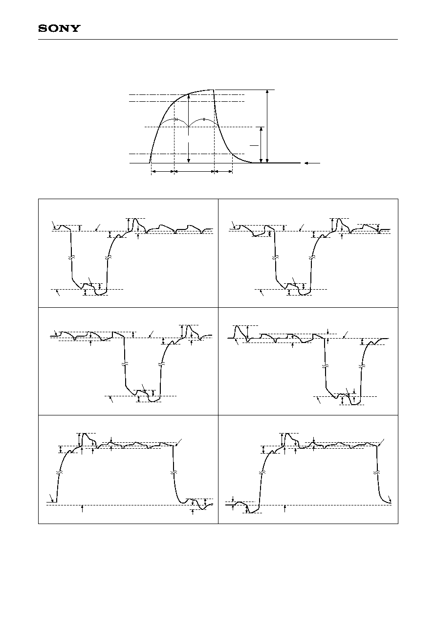
Drive Clock Waveform Conditions
(1) Readout clock waveform
V
VH
= (V
VH1
+ V
VH2
+ V
VH3
+ V
VH4
)/4
V
VL
= (V
VL5
+ V
VL6
)/2
V
V
= V
VH
n ≠ V
VL
n (n = 1 to 6)
(2) Vertical transfer clock waveform
V
1
V
2
V
3A
, V
3B
V
4
V
5A
, V
5B
V
6
100%
90%
10%
0%
tr
tf
0V
twh
M
2
M
V
VT
V
VH1
V
VHH
V
VH
V
VHL
V
VHH
V
VHL
V
VL1
V
VLH
V
VLL
V
VL
V
VH3
V
VHH
V
VH
V
VHL
V
VHH
V
VHL
V
VHL
V
VL3
V
VLH
V
VLL
V
VL
V
VH2
V
VHH
V
VHL
V
VH
V
VHL
V
VHH
V
VHL
V
VHH
V
VL2
V
VLH
V
VLL
V
VHH
V
VL
V
VHL
V
VHH
V
VHL
V
VHH
V
VH
V
VH5
V
VL
V
VL5
V
VHH
V
VH
V
VHL
V
VHL
V
VL4
V
VLH
V
VLL
V
VL
V
VH4
V
VLH
V
VLL
V
VHL
V
VLH
V
VLL
V
VHH
V
VHL
V
VHH
V
VH
V
VH6
V
VL
V
VL6
≠ 7 ≠
ICX432DQF
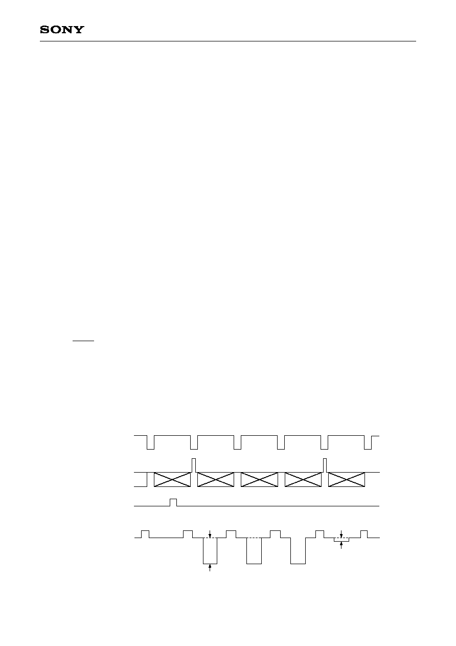
(3) Horizontal transfer clock waveform
Cross-point voltage for the H
1
rising side of the horizontal transfer clocks H
1
and H
2
waveforms is V
CR
.
The overlap period for twh and twl of horizontal transfer clocks H
1
and H
2
is two.
(4) Reset gate clock waveform
V
RGLH
is the maximum value and V
RGLL
is the minimum value of the coupling waveform during the period from
Point A in the above diagram until the rising edge of RG.
In addition, V
RGL
is the average value of V
RGLH
and V
RGLL
.
V
RGL
= (V
RGLH
+ V
RGLL
)/2
Assuming V
RGH
is the minimum value during the interval with twh, then:
V
RG
= V
RGH
≠ V
RGL
Negative overshoot level during the falling edge of RG is V
RGLm
.
(5) Substrate clock waveform
V
HL
V
CR
twl
two
twh
V
H
V
H
2
tr
H
2
90%
10%
H
1
tf
RG waveform
V
RGLH
V
RGH
V
RGL
V
RGLL
V
RGLm
tr
twh
twl
tf
V
RG
Point A
V
SUB
(A bias generated within the CCD)
100%
90%
10%
0%
tr
tf
twh
M
2
M
V
SUB
≠ 8 ≠
ICX432DQF
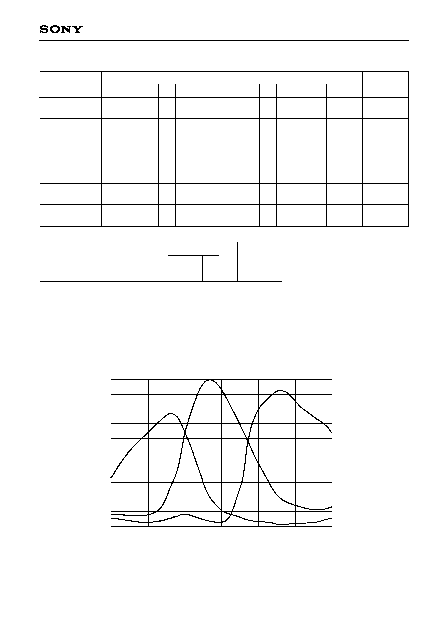
Spectral Sensitivity Characteristics (excludes lens characteristics and light source characteristics)
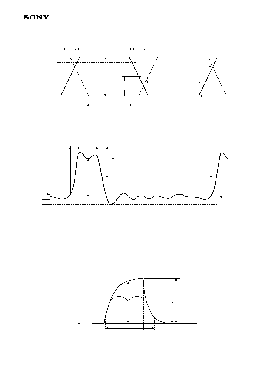
Clock Switching Characteristics (Horizontal drive frequency: 24.3MHz)
Min.
twh
Typ. Max. Min. Typ. Max. Min. Typ. Max. Min. Typ. Max.
twl
tr
tf
2.63
11
11
6
2.5
2.83
15
15
8
3.02
11
11
15
15
28
0.5
6.0
6.0
3
9.5
9.5
0.5
15
0.5
6.0
6.0
3
350
9.5
9.5
0.5
Unit
µs
ns
ns
ns
µs
Remarks
During
readout
When using
CXD3400N
tf
tr ≠ 2ns
During drain
charge
Item
Readout clock
Vertical transfer
clock
Horizontal
transfer clock
Reset gate clock
Substrate clock
Symbol
V
T
V
1
, V
2
,
V
3A
, V
3B
,
V
4
, V
5A
,
V
5B
, V
6
H
1
H
2
RG
SUB
Min.
two
Typ. Max.
10
15
Unit
ns
Remarks
Item
Horizontal transfer clock
Symbol
H
1
, H
2
400
1.0
B
G
R
0.9
0.8
0.7
0.6
0.5
0.4
0.3
0.2
0.1
0
450
500
550
Wave Length [nm]
Relativ
e Response
600
650
700
≠ 9 ≠
ICX432DQF
Image Sensor Characteristics (horizontal drive frequency: 24.3MHz)
(Ta = 25∞C)
1
After closing the mechanical shutter, the smear can be reduced to below the detection limit by performing
vertical register sweep operation.
2
Excludes vertical dark signal shading caused by vertical register high-speed transfer.
Zone Definition of Video Signal Shading
Measurement System
Note) Adjust the amplifier gain so that the gain between [
A] and [
B], and between [
A] and [
C] equals 1.
Item
G Sensitivity
Sensitivity
comparison
Saturation signal
Smear
Video signal shading
Dark signal
Dark signal shading
Line crawl G
Line crawl R
Line crawl B
Lag
Symbol
Sg
Rr
Rb
Vsat
Sm
SHg
Vdt
Vdt
Lcg
Lcr
Lcb
Lag
Min.
165
0.46
0.33
420
Typ.
220
≠87.5
≠78
Max.
275
0.72
0.59
≠80
≠70.5
20
25
10
8
3.8
3.8
3.8
0.5
Unit
mV
mV
dB
%
mV
mV
%
%
%
%
Measurement
method
1
1
1
2
3
4
5
6
7
7
7
8
Remarks
1/30s accumulation
Ta = 60∞C
Frame readout mode
1
High frame rate readout mode
Zone 0 and
I
Zone 0 to
II
'
Ta = 60∞C, 5.0 frame/s
Ta = 60∞C, 5.0 frame/s,
2
4
V
10
4
4
4
Ignored region
Effective pixel region
Zone 0,
I
Zone
II
,
II
'
V
10
H
8
H
8
2088 (H)
1550 (V)
CCD
C.D.S
S/H
S/H
AMP
CCD signal output [
A]
Gr/Gb channel signal output [
B]
R/B channel signal output [
C]
≠ 10 ≠
ICX432DQF
Image Sensor Characteristics Measurement Method
Measurement conditions
(1) In the following measurements, the device drive conditions are at the typical values of the bias and clock
voltage conditions, and the frame readout mode is used. In addition, V
SUB
Cont. is turned off.
(2) In the following measurements, spot blemishes are excluded and, unless otherwise specified, the optical
black level (OB) is used as the reference for the signal output, which is taken as the value of the Gr/Gb
channel signal output or the R/B channel signal output of the measurement system.
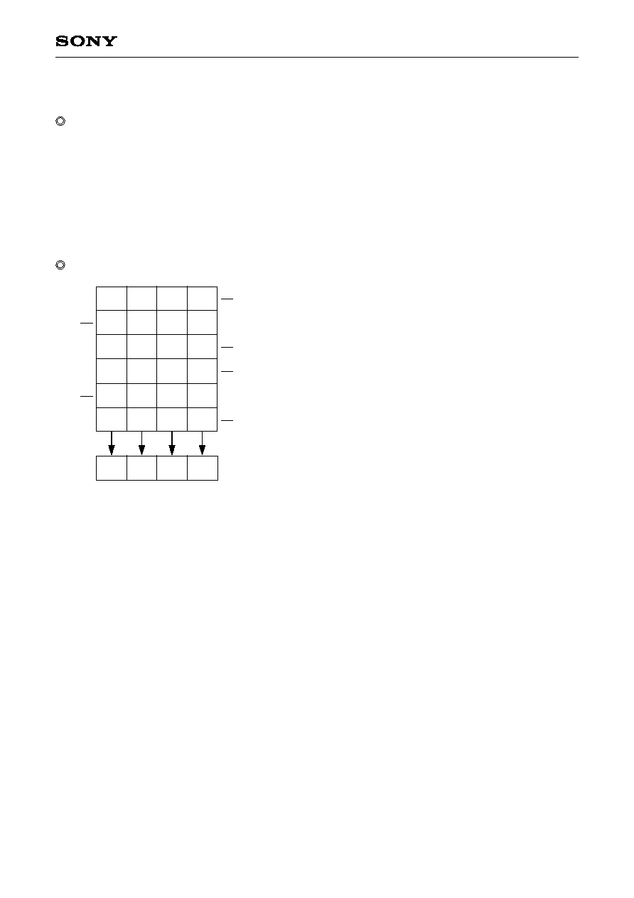
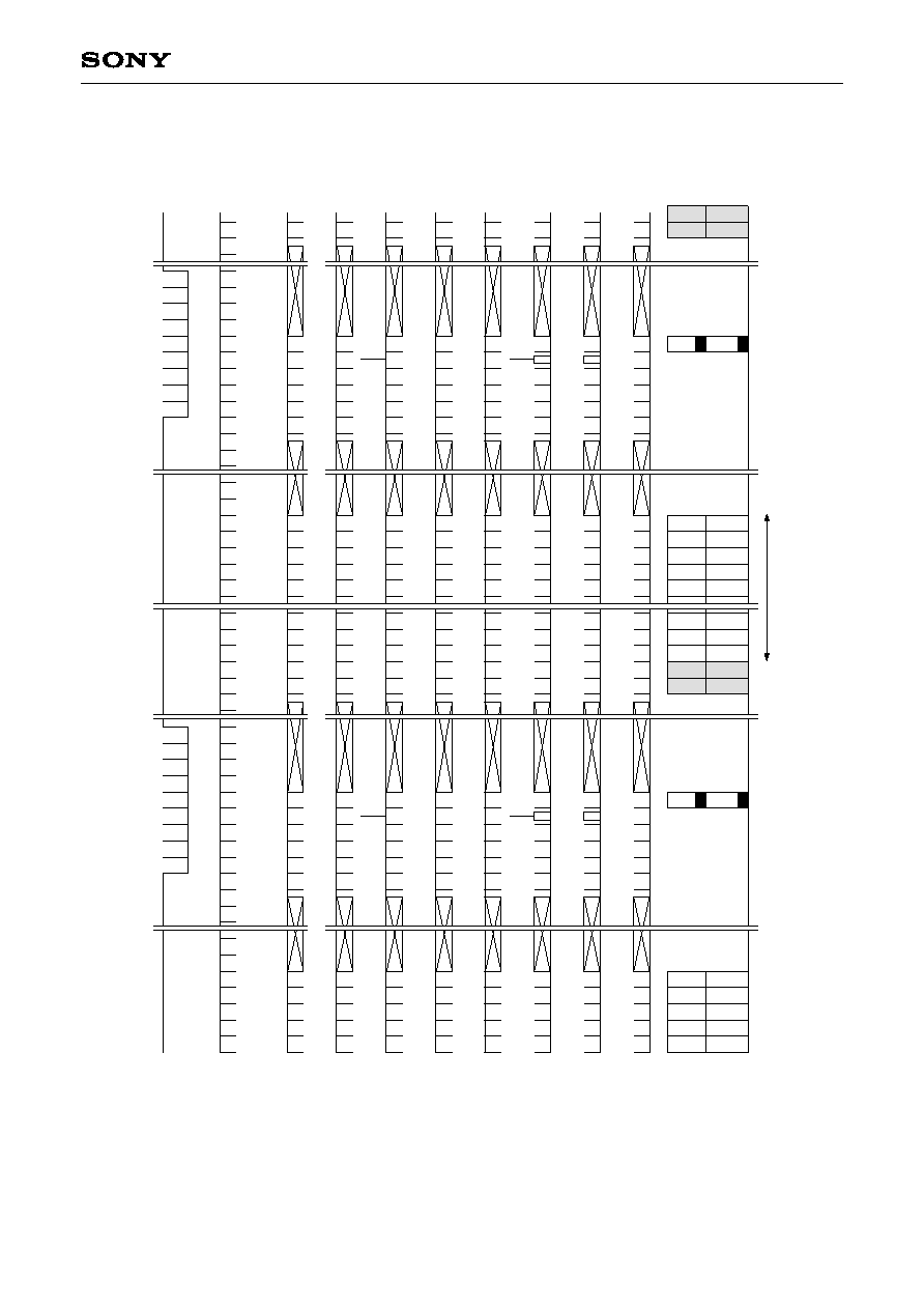
Color coding of this image sensor & Readout
The primary color filters of this image sensor are arranged in
the layout shown in the figure on the left (Bayer arrangement).
Gr and Gb denote the G signals on the same line as the R
signal and the B signal, respectively.
For three frames readout, the A1 and A2 lines are output as
signals in the A field, the B1 and B2 lines in the B field, and the
C1 and C2 lines in the C field.
Gb
B
Gb
B
R
Gr
R
Gr
Gb
B
Gb
B
R
Gr
R
Gr
B2
B1
A2
A1
Horizontal register
Color Coding Diagram
Gb
B
Gb
B
R
Gr
R
Gr
C2
C1
≠ 11 ≠
ICX432DQF
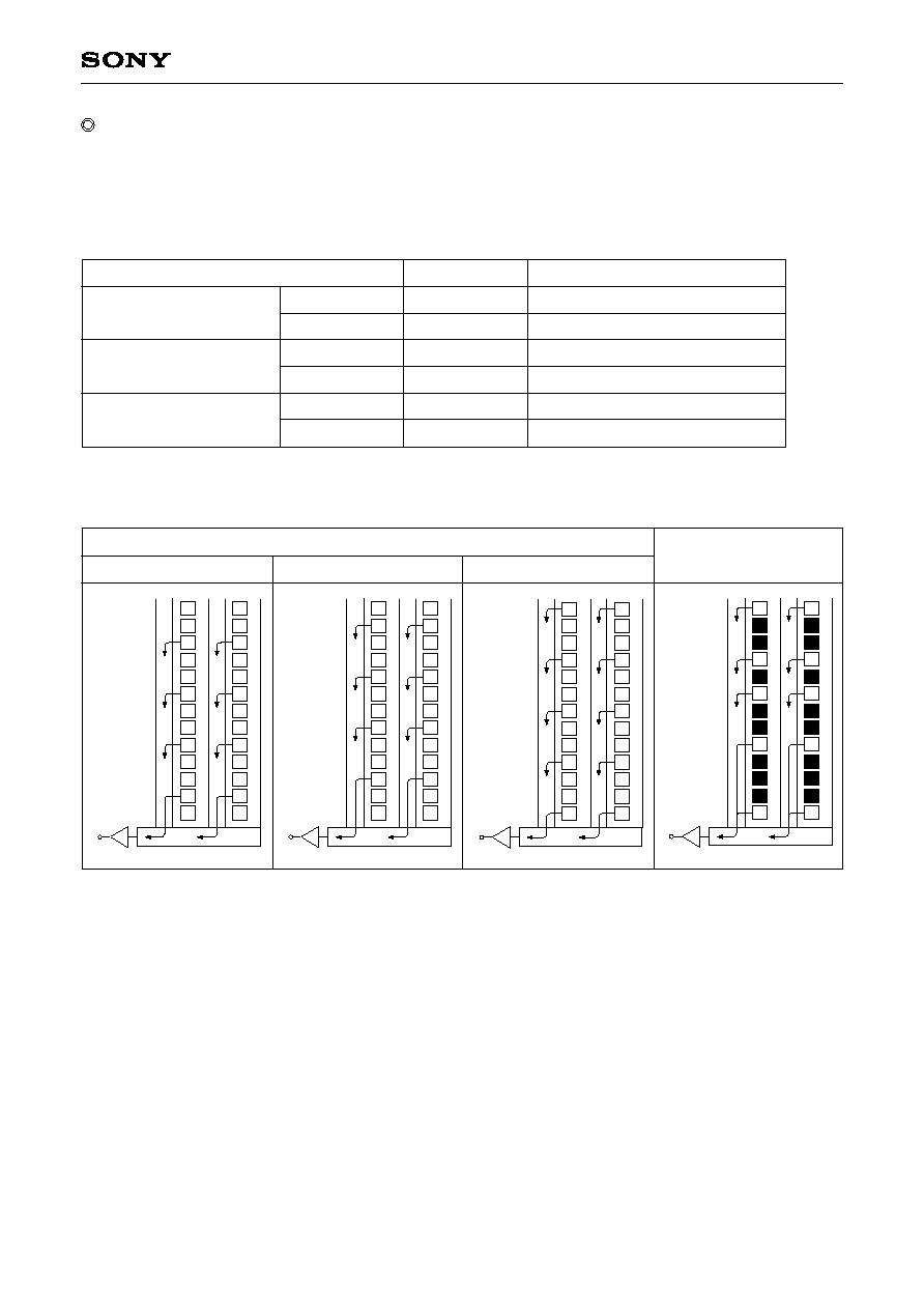
2. Frame readout mode, high frame rate readout mode
Readout modes
1. Readout modes list
The following readout modes are possible by driving the image sensor at the timing specifications noted in this
Data Sheet.
1. Frame readout mode
In this mode, all pixel signals are divided into three fields and output.
All pixel signals are read out independently, making this mode suitable for high resolution image capturing.
2. High frame rate readout mode
Output is performed at 30 frames per second by reading out 4 pixels for every 12 vertical pixels and adding
2 pixels in the horizontal CCD.
The number of output lines is 258 lines.
This readout mode emphasizes processing speed over vertical resolution.
Mode name
Frame rate
Number of effective output lines
Frame readout mode
High frame rate readout
mode
AF mode
NTSC mode
PAL mode
NTSC mode
PAL mode
NTSC mode
PAL mode
5.0 frame/s
5.0 frame/s
30 frame/s
25 frame/s
60 frame/s
50 frame/s
1550 (1st 517, 2nd 516, 3nd 517)
1550 (1st 517, 2nd 516, 3nd 517)
258
258
96
123
Frame readout mode
High frame rate readout
mode
1st field
Note) Blacked out portions in the diagram indicate pixels which are not read out.
2nd field
3rd field
13
12
11
10
9
8
7
6
5
4
3
1
2
V
OUT
R
Gb
R
Gb
R
Gb
R
Gb
R
Gb
R
R
Gb
Gr
B
Gr
B
Gr
B
Gr
B
Gr
B
Gr
Gr
B
13
12
11
10
9
8
7
6
5
4
3
1
2
V
OUT
R
Gb
R
Gb
R
Gb
R
Gb
R
Gb
R
R
Gb
Gr
B
Gr
B
Gr
B
Gr
B
Gr
B
Gr
Gr
B
13
12
11
10
9
8
7
6
5
4
3
1
2
V
OUT
R
Gb
R
Gb
R
Gb
R
Gb
R
Gb
R
R
Gb
Gr
B
Gr
B
Gr
B
Gr
B
Gr
B
Gr
Gr
B
13
12
11
10
9
8
7
6
5
4
3
1
2
V
OUT
R
Gb
R
Gb
R
R
Gb
Gb
R
R
Gb
Gr
B
Gr
B
Gb
B
Gr
Gr
B
B
Gr
Gr
B
R
Gr
≠ 12 ≠
ICX432DQF
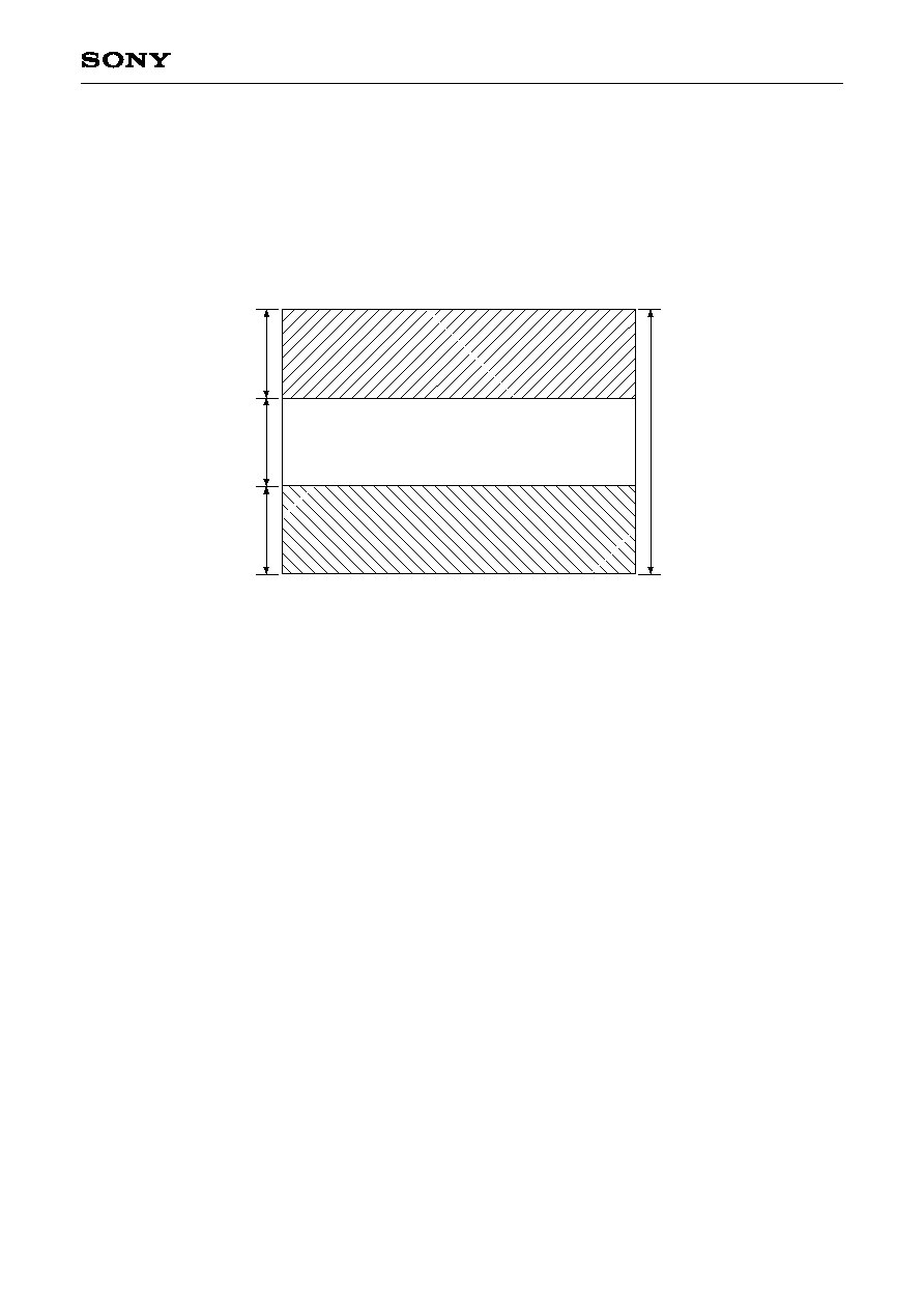
3. AF
The AF mode increases the frame rate by cutting out a portion of the picture through high-speed elimination of
the top and bottom of the picture in high frame rate readout mode. This mode allows 1/60s and 1/50s output,
so it is effective for raising the auto focus (AF) speed.
In addition, the output line position and number of output lines are fixed. See the timing specifications for the
cut-out region.
Number of effective lines
in high frame rate
readout mode
258
Top
frame shift region
Cut-out region
Bottom
high-speed sweep region

≠ 13 ≠
ICX432DQF
Definition of standard imaging conditions
(1) Standard imaging condition
I
:
Use a pattern box (luminance: 706cd/m
2
, color temperature of 3200K halogen source) as a subject.
(Pattern for evaluation is not applicable.) Use a testing standard lens with CM500S (t = 1.0mm) as an IR
cut filter and image at F5.6. The luminous intensity to the sensor receiving surface at this point is defined
as the standard sensitivity testing luminous intensity.
(2) Standard imaging condition
II
:
Image a light source (color temperature of 3200K) with a uniformity of brightness within 2% at all angles.
Use a testing standard lens with CM500S (t = 1.0mm) as an IR cut filter. The luminous intensity is adjusted
to the value indicated in each testing item by the lens diaphragm.
(3) Standard imaging condition
III
:
Image a light source (color temperature of 3200K) with a uniformity of brightness within 2% at all angles.
Use a testing standard lens (exit pupil distance ≠33mm) with CM500S (t = 1.0mm) as an IR cut filter. The
luminous intensity is adjusted to the value indicated in each testing item by the lens diaphragm.
1. G Sensitivity, sensitivity comparison
Set to the standard imaging condition
I
. After setting the electronic shutter mode with a shutter speed of
1/100s, measure the signal outputs (V
GR
, V
Gb
, V
R
and V
B
) at the center of each Gr, Gb, R and B channel
screen, and substitute the values into the following formulas.
V
G
= (V
Gr
+ V
Gb
)/2
Sg = V
G
◊
[mV]
Rr = V
R
/V
G
Rb = V
B
/V
G
2. Saturation signal
Set to the standard imaging condition
II
. After adjusting the luminous intensity to 20 times the intensity with
the average value of the Gr signal output, 150mV, measure the minimum values of the Gr, Gb, R and B
signal outputs.
3. Smear
Set to the standard imaging condition
III
. With the lens diaphragm at F5.6 to F8, first adjust the average
value of the Gr signal output to 150mV. Measure the average values of the Gr signal output, Gb signal
output, R signal output and B signal output (Gra, Gba, Ra, Ba), and then adjust the luminous intensity to
500 times the intensity with the average value of the Gr signal output, 150mV.
After the readout clock is stopped and the charge drain is executed by the electronic shutter at the
respective H blankings, measure the maximum value (Vsm [mV]) independent of the Gr, Gb, R and B
signal outputs, and substitute the values into the following formula.
Sm = 20
◊
log
(
Vsm
˜
◊
◊
)
[dB] (1/10V method conversion value)
1
10
1
500
Gra + Gba + Ra + Ba
4
100
30
≠ 14 ≠
ICX432DQF
4. Video signal shading
Set to the standard imaging condition
III
. With the lens diaphragm at F5.6 to F8, adjusting the luminous
intensity so that the average value of the Gr signal output is 150mV. Then measure the maximum value
(Grmax [mV]) and minimum value (Grmin [mV]) of the Gr signal output and substitute the values into the
following formula.
SHg = (Grmax ≠ Grmin)/150
◊
100 [%]
5. Dark signal
Measure the average value of the signal output (Vdt [mV]) with the device ambient temperature of 60∞C
and the device in the light-obstructed state, using the horizontal idle transfer level as a reference.
6. Dark signal shading
After measuring 5, measure the maximum (Vdmax [mV]) and minimum (Vdmin [mV]) values of the dark
signal output and substitute the values into the following formula.
Vdt = Vdmax ≠ Vdmin [mV]
7. Line crawl
Set to the standard imaging condition
II
. Adjusting the luminous intensity so that the average value of the
Gr signal output is 150mV, and then insert R, G and B filters and measure the difference between G signal
lines (
Glr,
Glg,
Glb [mV]) as well as the average value of the G signal output (Gar, Gag, Gab).
Substitute the values into the following formula.
Lci =
◊
100 [%] (i = r, g, b)
8. Lag
Adjust the Gr signal output value generated by the strobe light to 150mV. After setting the strobe light so
that it strobes with the following timing, measure the residual signal amount (Vlag). Substitute the value
into the following formula.
Lag = (Vlag/150)
◊
100 [%]
Gli
Gai
Light
VD
V3A/V3B
Strobe light timing
Output
Vlag (lag)
Gr signal output 150mV
≠ 15 ≠
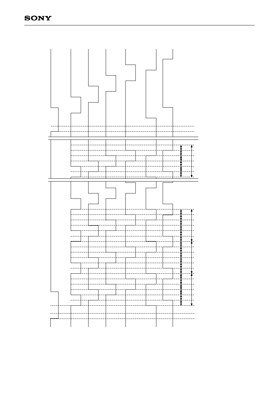
ICX432DQF
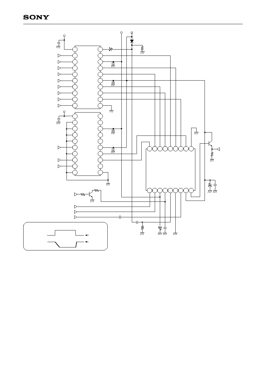
Drive Circuit
Notes) Substrate bias control
1. The saturation signal level decreases when exposure is performed using the mechanical shutter,
so control the substrate bias.
2. A saturation signal level equivalent to that for continuous exposure can be assured by connecting
a VR1 grounding registor to the CCD C
SUB
pin.
Drive timing precautions
1. Blooming occurs in modes (high frame rate readout, etc.) that do not use the mechanical shutter,
so do not ground the connected VR1 resistor.
2. tf is slow, so the internally generated voltage V
SUB
may not drop to a sufficiently low level if the
substrate bias control signal is not set to high level 30ms before entering the exposure period
and the VR1 resistor connected to the C
SUB
pin is not grounded.
3. The blooming signal generated during exposure in mechanical shutter mode is swept by providing
two fields or more of idle transfer through vertical register high-speed sweep transfer from the
time the mechanical shutter closes until sensor readout is performed. However, note that the V
L
potential and the
SUB pin DC voltage sag at this time.
Substrate bias
control signal
V
SUB
Cont.
Mechanical
shutter mode
Substrate bias
SUB pin voltage
GND
tr
2ms
tf
17ms
Internally
generated
value V
SUB
XSUB
XV3
XSG3B
XSG3A
XV5
XSG5B
XSG5A
XV4
XV1
XSG1
XV6
XV2
V
SUB
Cont.
H
2
H
1
RG
0.1
0.1
0.1
0.1
0.1
0.1
1M
0.1
0.01
3.3/20V
0.1
4.7k
100k
CCD OUT
VR1 (3.9k
)
20
19
18
17
16
15
14
13
12
11
1
2
3
4
5
6
7
8
9
10
CXD3400N
20
19
18
17
16
15
14
13
12
11
1
2
3
4
5
6
7
8
9
10
CXD3400N
1
2
3
4
5
6
7
8
9
18 17 16 15 14 13 12 11 10
ICX432DQF
(BOTTOM VIEW)
3.3/16V
1/35V
3.3V
0.1
3.3V
≠7.5V
15V
V
DD
V
OUT
GND
H
2
H
1
V
L
C
SUB
SUB
RG
V
1
GND
V
6
V
5B
V
5A
V
4
V
3B
V
2
V
3A
2SC4250
≠ 16 ≠
ICX432DQF
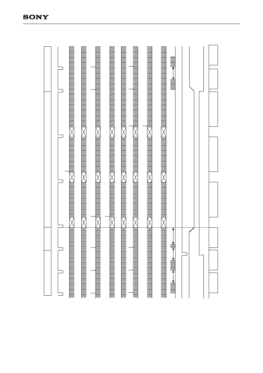
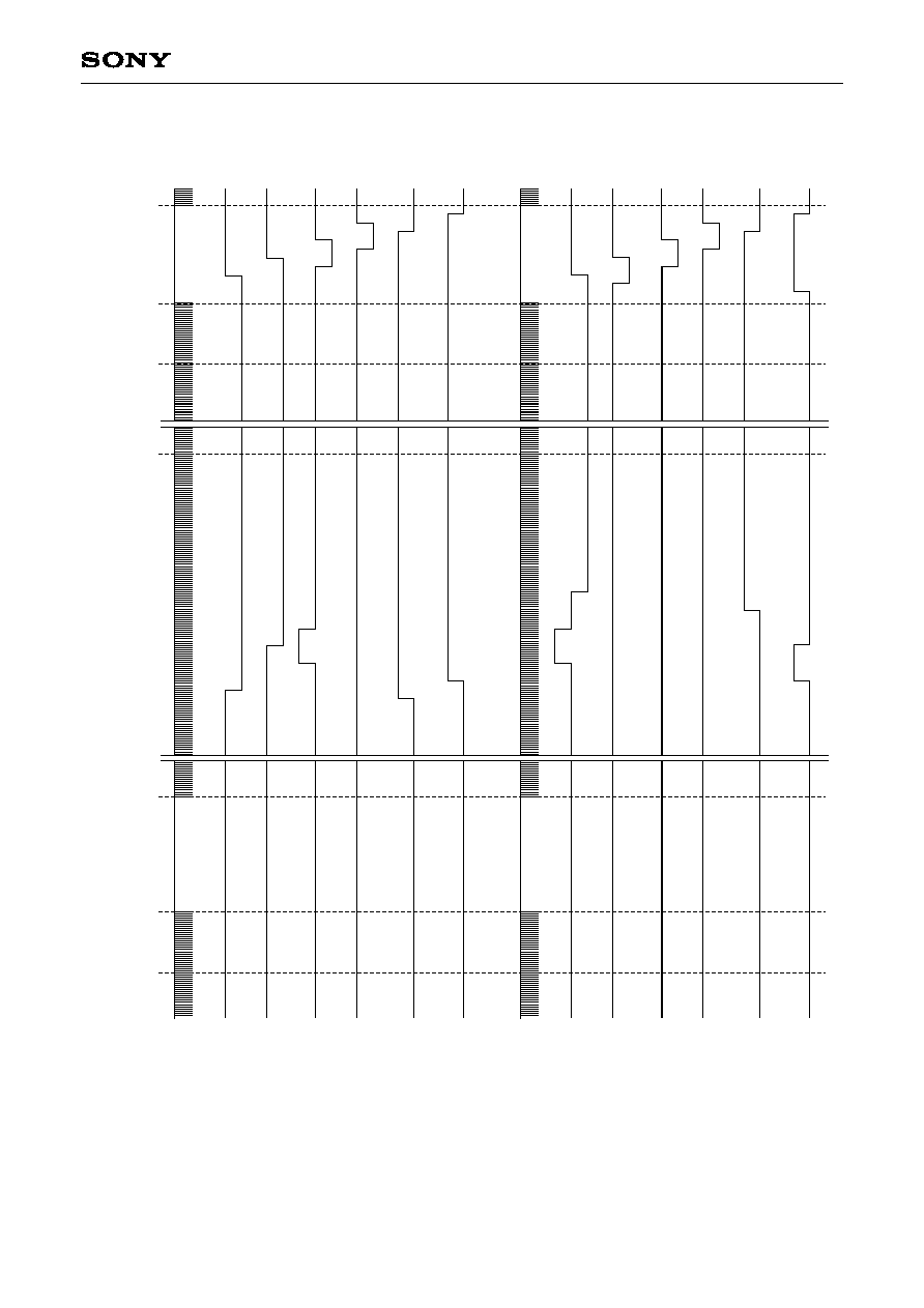
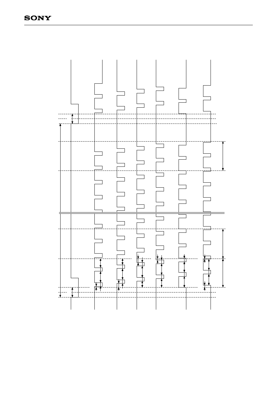
Drive
Timing
Char
t (V
e
r
tical
Sequence)
High Frame Rate Readout Mode
Frame Readout Mode/Electr
onic Shutter Normal Operation
Note)
High frame rate readout mode out signals of
V
SUB
Cont.
high per
iod contain a b
l
ooming component and should theref
ore not be used.
Apply 20 or more electronic shutter pulses at the star
t of e
xposure f
or the recording image
.
If less than 20 pulses are applied, the electronic shutter ma
y occur a discharge error
.
B
OPEN
VD
V1
V2
V3A
V3B
V4
V5A
V5B
V6
SUB
TRG
CLOSE
BC
E
High fr
ame r
ate readout mode
High fr
ame r
ate readout mode
A signal
output
F
r
ame readout mode
Exposure oper
ation
Mechanical
shutter
V
SUB
Cont.
CCD
OUT
B signal
output
B signal
output
E signal
output
Output after
fr
ame readout
C signal output (1st)
C signal output (2nd)
C signal output (3rd)
≠ 17 ≠
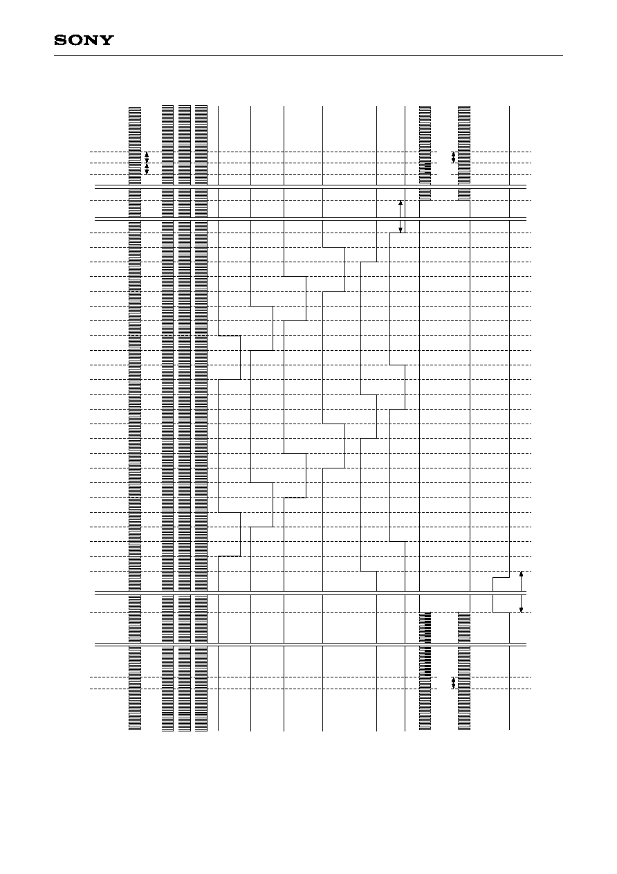
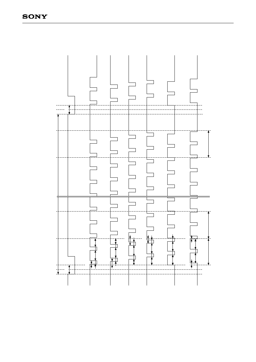
ICX432DQF
Drive
Timing
Char
t
(V
er
tical
Sync)
NTSC/P
AL Frame Readout Mode
NTSC:
5.0 frame/s,
P
AL:
5.0 frame/s
Note)
2760fH, ho
we
v
e
r
,
588H, 1176H and 1764H in NTSC mode are 1500clk, 705H, 1410H and 2115H in P
AL mode are 960clk.
1548
1545
2
5
8
3
6
9
1549
1546
3
6
1
4
VD
Exposure per
iod
"a"
"b"
"c"
HD
PA
L
V1
V2
V3A
V3B
V4
V5A
V5B
V6
SUB
OPEN
CLOSE
1550
1547
1
4
7
2
5
8
TRG
Mechanical
shutter
CCD
OUT
NTSC
1
1
9
9
41
41
44
44
564
564
705
588
746
629
749
632
1269
1152
1410
1176
1451
1217
1454
1220
1975
1741
2115
1764
V
SUB
Cont.
≠ 18 ≠
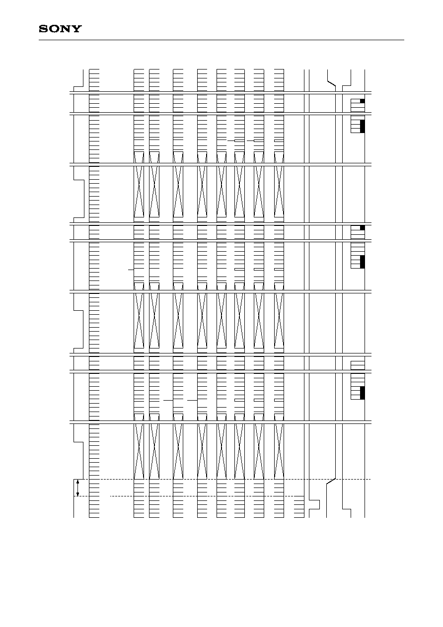
ICX432DQF
Drive
Timing Char
t
(Readout)
NTSC/P
AL Frame Readout Mode
"a" Enlar
g
e
d
"b" Enlar
g
e
d
1296
2760
H1
V1
V2
V3A/V3B
NTSC
44H
P
A
L
44H
NTSC
632H
P
A
L
749H
V4
V5A/V5B
V6
2760
1
52
644
1
52
644
308
1420
392
434
560
1380
1460
350
476
1338
602
1254
518
2760
H1
V1
V2
V3A/V3B
V4
V5A/V5B
V6
2760
1
52
644
1
644
266
392
434
560
350
476
1338
1420
602
224
1502
518
1380
1460
1546
308
≠ 19 ≠
ICX432DQF
Drive
Timing Char
t
(Readout)
NTSC/P
AL Frame Readout Mode
"c" Enlar
g
e
d
1128
2760
H1
V1
V2
V3A/V3B
V4
V5A/V5B
V6
2760
1
52
644
1
52
644
1254
1212
1338
1296
476
1420
560
1380
1460
518
1086
1170
602
NTSC
1220H
P
A
L
1454H
≠ 20 ≠
ICX432DQF
Drive
Timing
Char
t
(High-speed
Sweep
Operation)
NTSC/P
AL Frame Readout Mode
Note)
In the per
iod of high-speed s
w
eep oper
ation, the r
ising of input cloc
ks XV1, XV2, XV3, XV4, XV5 and XV6 to v
e
r
tical transf
er cl
oc
k dr
i
v
er CD3400N should be
dela
y
ed b
y
1 cloc
k against the abo
v
e
timing char
t.
18
18
18
18
18
#1040
18
18
18
18
18
18
18
18
18
18
18
18
18
18
18
18
18
18
#3
#2
#1
140
52
1
52
1
18
HD
V1
V2
V3A/V3B
V4
V5A/V5B
V6
≠ 21 ≠
ICX432DQF
Drive
Timing
Char
t
(Horizontal
Sync)
NTSC/P
AL Frame Readout Mode
CLK
2760
1
5
18
3
52
48
1
1
644
592
1
28
4
4
RG
SHP
SHD
V1
V2
V3A/V3B
V4
V5A/V5B
V6
H1
H2
SUB
1
126
1
1
382
84
1
126
1
1
298
168
1
126
1
1
214
252
1
126
1
1
130
336
88
1
1
378
11
2
6
172
1
1
1
42
378
88
Ignored pix
e
l 4 bits
Ignored pix
e
l 4 bits
≠ 22 ≠
ICX432DQF
Drive
Timing
Char
t
(V
er
tical
Sync)
NTSC/P
AL High Frame Rate Readout Mode
NTSC:
30 frame/s,
P
AL:
25 frame/s
Note)
3004fH, howe
v
e
r
,
270H in NTSC mode is 2734fH, 324H in P
AL mode is 1708fH.
NTSC
VD
HD
V1
V2
V3A
V3B
V4
V5A
V5B
CCD
OUT
V6
263
263
270
324
1
1
9
9
263
263
270
324
1
1
4
4
9
9
PA
L
6
4
5
1
10
8
17
13
22
20
29
25
34
32
6
4
5
1
10
8
17
13
22
20
29
25
34
32
1534
1541
1546
1532
1537
1544
1549
1534
1541
1546
1532
1529
1525
1537
1544
1549
≠ 23 ≠
ICX432DQF
Drive
Timing
Char
t (Readout P
o
r
tion)
NTSC/P
AL High Frame Rate Readout Mode/AF Mode
H1
V1
V2
V3A
V3B
V4
V5A
V5B
V6
1
1438
1611
888
52
888
52
1
3004
1
1540
1673
1500
1580
1704
1784
1
1642
1815
1
1
1744
1877
1642
1815
1
1407
1
846
1
1407
1
846
1
1469
1908
1
≠ 24 ≠
ICX432DQF
Drive
Timing
Char
t
(Horizontal
Sync)
NTSC/P
AL High Frame Rate Readout Mode/AF Mode
CLK
3004
1
5
3004
18
3
1
5
52
48
1
1
888
836
1
28
4
4
RG
SHP
SHD
V1
V2
V3A/V3B
V4
V5A/V5B
V6
H1
H2
SUB
19
3
1
1
119
19
3
1
279
252
19
3
1
1
181
19
3
1
279
190
19
3
1
1
243
19
3
1
279
128
19
3
1
1
305
19
3
1
279
66
19
3
88
1
1
1
279
19
7
279
19
3
150
1
1
1
279
35
279
88
Ignored pix
e
l 4 bits
Ignored pix
el 4 bits
52
≠ 25 ≠
ICX432DQF
Drive Timing
Char
t
(V
er
tical
Sync)
AF
Mode
NTSC:
60 frame/s,
P
AL:
50 frame/s
Note)
3004fH, howe
v
e
r
,
135H in NTSC mode is 2869clk, and 162H in P
AL mode is 2356clk.
VD
HD
V1
V2
V3A
V3B
V4
V5A
V5B
CCD
OUT
V6
6
4
6
4
485
481
490
488
AF mode output signal
NTSC
96 lines
P
A
L
123 lines
NTSC
123
150
135
162
1
1
4
4
9
9
25
25
28
28
123
150
135
162
1
1
4
4
9
9
25
25
PA
L
High-speed s
w
eep per
iod
High-speed s
w
eep per
iod
F
r
ame shift per
iod
F
r
ame shift per
iod
≠ 26 ≠
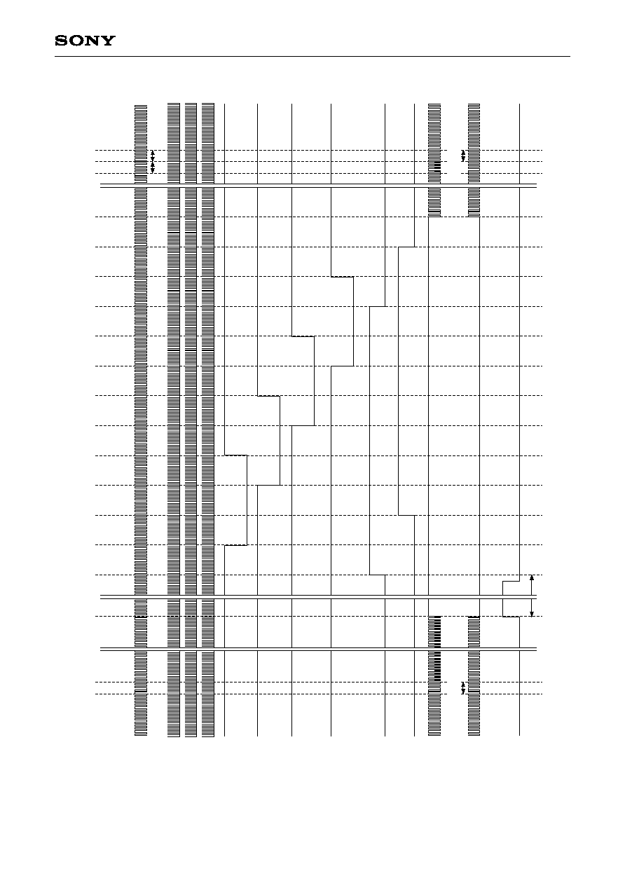
ICX432DQF
Drive
Timing Char
t (High-speed Frame Shift Operation)
NTSC/P
AL
AF
Mode
93
279
1
93
248
93
279
93
186
155
93
93
279
217
93
93
279
279
93
93
279
279
#1
AF:
#78
#2
93
279
140
1
140
31
93
AF mode 20H
HD
V1
V2
V3A/V3B
V4
V5A/V5B
V6
124
62
31
62
≠ 27 ≠
ICX432DQF
Drive
Timing Char
t (High-speed Frame Sweep Operation)
NTSC/P
AL
AF
Mode
36
108
1
36
96
36
108
36
72
60
36
36
108
84
36
36
108
108
36
36
108
108
#1
AF:
#114
#2
36
108
140
1
140
12
36
AF mode 11H
HD
V1
V2
V3A/V3B
V4
V5A/V5B
V6
48
24
12
24
≠ 28 ≠
ICX432DQF
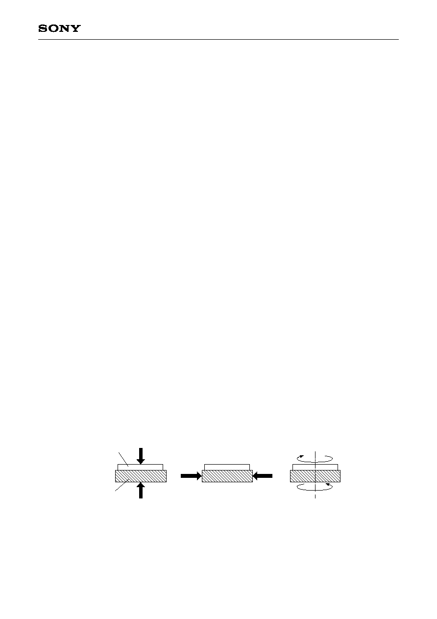
Notes on Handling
1) Static charge prevention
CCD image sensors are easily damaged by static discharge. Before handling be sure to take the following
protective measures.
a) Either handle bare handed or use non-chargeable gloves, clothes or material.
Also use conductive shoes.
b) When handling directly use an earth band.
c) Install a conductive mat on the floor or working table to prevent the generation of static electricity.
d) Ionized air is recommended for discharge when handling CCD image sensors.
e) For the shipment of mounted substrates, use boxes treated for the prevention of static charges.
2) Soldering
a) Make sure the package temperature does not exceed 80∞C.
b) Solder dipping in a mounting furnace causes damage to the glass and other defects. Use a 30W
soldering iron with a ground wire and solder each pin in less than 2 seconds. For repairs and remount,
cool sufficiently.
c) To dismount an image sensor, do not use a solder suction equipment. When using an electric desoldering
tool, use a thermal controller of the zero-cross On/Off type and connect it to ground.
3) Dust and dirt protection
Image sensors are packed and delivered by taking care of protecting its glass plates from harmful dust and
dirt. Clean glass plates with the following operations as required, and use them.
a) Perform all assembly operations in a clean room (class 1000 or less).
b) Do not either touch glass plates by hand or have any object come in contact with glass surfaces. Should
dirt stick to a glass surface, blow it off with an air blower. (For dirt stuck through static electricity ionized
air is recommended.)
c) Clean with a cotton bud and ethyl alcohol if grease stained. Be careful not to scratch the glass.
d) Keep in a case to protect from dust and dirt. To prevent dew condensation, preheat or precool when
moving to a room with great temperature differences.
e) When a protective tape is applied before shipping, just before use remove the tape applied for
electrostatic protection. Do not reuse the tape.
4) Installing (attaching)
a) Remain within the following limits when applying a static load to the package. Do not apply any load
more than 0.7mm inside the outer perimeter of the glass portion, and do not apply any load or impact to
limited portions. (This may cause cracks in the package.)
b) If a load is applied to the entire surface by a hard component, bending stress may be generated and the
package may fracture, etc., depending on the flatness of the bottom of the package. Therefore, for
installation, use either an elastic load, such as a spring plate, or an adhesive.
Plactic package
Cover glass
Compressive strength
50N
50N
1.2Nm
Torsional strength

≠ 29 ≠
ICX432DQF
c) The adhesive may cause the marking on the rear surface to disappear, especially in case the regulated
voltage value is indicated on the rear surface. Therefore, the adhesive should not be applied to this area,
and indicated values should be transferred to other locations as a precaution.
d) The notch of the package is used for directional index, and that can not be used for reference of fixing.
In addition, the cover glass and seal resin may overlap with the notch of the package.
e) If the leads are bent repeatedly and metal, etc., clash or rub against the package, the dust may be
generated by the fragments of resin.
f) Acrylate anaerobic adhesives are generally used to attach CCD image sensors. In addition, cyano-
acrylate instantaneous adhesives are sometimes used jointly with acrylate anaerobic adhesives.
(reference)
5) Others
a) Do not expose to strong light (sun rays) for long periods, as color filters will be discolored. When high
luminous objects are imaged with the exposure level controlled by the electronic iris, the luminance of
the image-plane may become excessive and discoloring of the color filter will possibly be accelerated. In
such a case, it is advisable that taking-lens with the automatic-iris and closing of the shutter during the
power-off mode should be properly arranged. For continuous using under cruel condition exceeding the
normal using condition, consult our company.
b) Exposure to high temperature or humidity will affect the characteristics. Accordingly avoid storage or
usage in such conditions.
c) Brown stains may be seen on the bottom or side of the package. But this does not affect the CCD
characteristics.
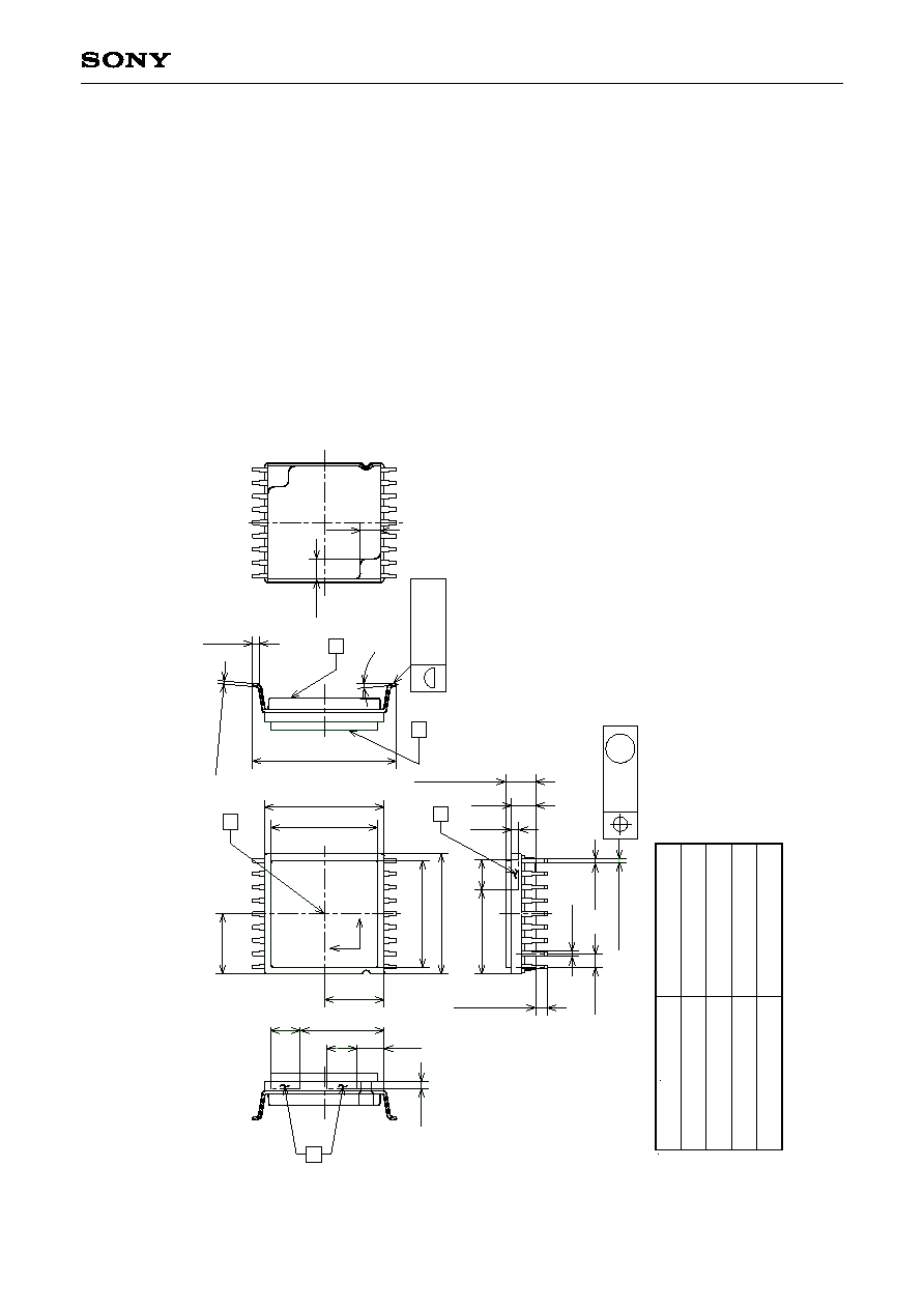
≠ 30 ≠
ICX432DQF
Sony Corporation
P
a
c
k
a
g
e Outline
Unit:
mm
P
A
CKA
GE MA
TERIAL
LEAD TREA
TMENT
LEAD MA
TERIAL
P
A
CKA
GE MASS
DRA
WING NUMBER
Plastic
GOLD PLA
TING
0.5g
42 ALLO
Y
AS-C15-02(E)
18 pin SOP (400mil)
M
0.3
(0.6)
0.25 ± 0.05
12.0 ± 0.15
8.9
8.9
10.0 ± 0.10
10.0 ± 0.10
1.0 ± 0.10
0.38
0.46
1.11
2.5
7.0
2.3
0.6
2.5
B
5.0
10
18
5.0
V
H
1
9
A
C
D
0∞ to 10∞
10
18
9
1
1.7
1.7
B'
7.0
2.5
0.6
2.0
2.50 ± 0.15
0.30 ± 0.15
1.
"A"
is the center of the eff
ectiv
e image area.
2.
The tw
o points
"B"
of the pac
kage are the hor
iz
ontal ref
erence
.
The point
"B'"
of the pac
kage is the v
e
r
tical ref
erence
.
3.
The bottom
"C"
of the pac
kage
, and the top of the co
v
er glass
"D"
are the height ref
erence
.
4.
The center of the eff
ectiv
e image area relativ
e to
"B"
and
"B'"
is (H,
V) = (5.0, 5.0) ± 0.07mm.
5.
The rotation angle of the eff
ectiv
e image area relativ
e to H and
V is ± 0.8∞.
6.
The height from the bottom
"C"
to the eff
ectiv
e image area is 1.20 ± 0.10mm.
The height from the top of the co
v
er glass
"D"
to the eff
ectiv
e image area is 1.30 ± 0.15mm.
7.
The tilt of the eff
ectiv
e image area relativ
e to the bottom
"C"
is less than 25µm.
The tilt of the eff
ectiv
e image area relativ
e to the top
"D"
of the co
v
er glass is less than 25µm.
8.
The thic
kness of the co
v
er glass is 0.5mm, and the refr
activ
e inde
x is 1.5.
9.
The notch of the pac
kage is used only f
or directional inde
x, that m
ust not be used f
or ref
erence
of fixing.
0.15