≠ 1 ≠
ILX520K
24 pin DIP
E96539-ST
7078
◊
3pixel CCD Linear Sensor (Color)
Description
The ILX520K is a reduction type CCD linear sensor
developing for color image scanner. This sensor reads
A3-size documents at a density of 600 DPI.
Features
∑ Number of effective pixels: 21234 pixels
(7078 pixels
◊
3)
∑ Pixel size:
8µm
◊
8µm (8µm pitch)
∑ Distance between line:
64µm (8 Lines)
∑ Single-sided readout
∑ Ultra low lag / Ultra high sensitivity
∑ Single 12V power supply
∑ Input clock pulse:
CMOS 5V drive
∑ Number of output
3 (R, G, B)
∑ Package:
24 pin DIP (400 mil)
Absolute Maximum Ratings
∑ Supply voltage
V
DD
15
V
∑ Operating temperature
≠10 to +55
∞C
∑ Storage temperature
≠30 to +80
∞C
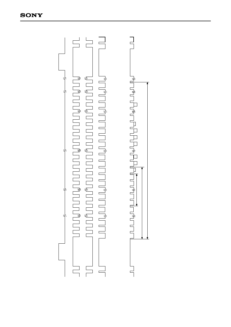
Pin Configuration (Top View)
Block Diagram
Sony reserves the right to change products and specifications without prior notice. This information does not convey any license by
any implication or otherwise under any patents or other right. Application circuits shown, if any, are typical examples illustrating the
operation of the devices. Sony cannot assume responsibility for any problems arising out of the use of these circuits.
2
3
4
5
6
7
8
9
10
11
12
13
14
15
16
17
18
19
20
21
22
1
7078
R
1
7078
G
1
7078
B
1
V
OUT-G
V
OUT-B
V
DD
NC
NC
2
V
DD
2
NC
ROG
-B
ROG
-G
V
OUT-R
GND
RS
LH
GND
1
NC
1
NC
ROG
-R
GND
NC
23
24 NC
16
3
2
D14
D15
D63
S1
D64
D75
Read Out Gate
CCD Register
S7078
Driver
D14
D15
D63
S1
D64
D75
Read Out Gate
CCD Register
S7078
Driver
D14
D15
D63
S1
D64
D75
Read Out Gate
CCD Register
S7078
Driver
Driver
Blue
Green
Red
ROG
-B
ROG
-G
ROG
-R
V
OUT-B
V
OUT-G
V
OUT-R
V
DD
LH
V
DD
2
GND
RS
1
1
GND
2
17
6
13
4
7
9
11
12
14
18
21
22
23
GND
5
For the availability of this product, please contact the sales office.
≠ 3 ≠
ILX520K
Electrooptical Characteristics (Note 1)
Ta = 25∞C, V
DD
= 12V, f
RS
= 1MHz, Input clock = 5Vp-p, Light source = 3200K, IR cut filter CM-500S (t = 1.0mm)
Item
Symbol
Min.
Typ.
Max.
Unit
Remarks
Sensitivity
Sensitivity nonuniformity
Saturation output voltage
Saturation
exposure
Dark voltage average
Dark signal nonuniformity
Image lag
Supply current
Total transfer efficiency
Output impedance
Offset level
Dynamic range
R
R
R
G
R
B
PRNU
V
SAT
SE
R
SE
G
SE
B
V
DRK
DSNU
IL
I
VDD
TTE
Z
O
V
OS
DR
1.3
2.1
1.6
--
2
0.74
0.46
0.58
--
--
--
--
92
--
--
1000
2.0
3.2
2.5
4
3.2
1.6
1
1.28
0.3
1.5
0.02
26
98
250
6.5
10670
2.7
4.3
3.4
20
--
--
--
--
2
5
--
50
--
--
--
--
V/(lx ∑ s)
%
V
lx ∑ s
mV
mV
%
mA
%
V
--
Note 2
Note 3
Note 4
Note 5
Note 6
Note 6
Note 7
--
--
--
Note 8
Note 9
Red
Green
Blue
Red
Green
Blue
Note
1) In accordance with the given electrooptical characteristics, the black level is defined as the average value
of D2, D3 to D12.
2) For the sensitivity test light is applied with a uniform intensity of illumination.
3) PRNU is defined as indicated below. Ray incidence conditions are the same as for Note 2.
V
OUT
= 500mV (Typ.)
PRNU =
◊
100 [%]
Where the 7078 pixels are divided into blocks of 114 (Last block is 124 pixel). The maximum output of
each block is set to V
MAX
, the minimum output to V
MIN
and the average output to V
AVE
.
4) Use below the minimum value of the saturation output voltage.
5) Saturation exposure is defined as follows.
SE =
Where R indicates R
R
, R
G
, R
B
, and SE indicates SE
R
, SE
G
, SE
B
.
6) Optical signal accumulated time
int stands at 10ms.
7) V
OUT
= 500mV (Typ.)
8) Vos is defined as indicated bellow.
V
OUT
indicates V
OUT-R
, V
OUT-G
, and V
OUT-B
.
9) Dynamic range is defined as follows.
DR =
When the optical signal accumulated time is shorter, the dynamic range gets wider because the optical
signal accumulated time is in proportion to the dark voltage.
(V
MAX
≠ V
MIN
) /2
V
AVE
V
OS
V
OUT
GND
V
SAT
R
V
SAT
V
DRK
≠ 4 ≠
ILX520K
2
1
3
4
7153
D1
D2
D3
D13
D14
D15
D61
D62
D63
S1
S2
S7076
S7077
S7078
D64
D65
D70
D71
D75
Optical black (49 pixels)
Dummy signal (63 pixels)
1-line output period (7153 pixels)
ROG
1
LH
2
RS
V
OUT
5
0
5
0
5
0
5
0
Clock Timing Chart 1
Note)
The transfer pulses (
1,
2,
LH) must have more than 7153 cycles.