Description
The ILX526A is a rectangular reduction type CCD
linear image sensor designed for bar code POS
hand scanner and optical measuring equipment use.
A built-in timing generator and clock-drivers ensure
single 5V power supply for easy use.
Features
∑ Number of effective pixels: 3000 pixels
∑ Pixel size: 7µm
◊
200µm (7µm pitch)
∑ Single 5V power supply
∑ High sensitivity: 300V/(lx ∑ s)
∑ Built-in timing generator and clock-drivers
∑ Built-in sample-and-hold circuit
∑ Electrical shutter function
∑ Clock frequency: 100kHz (Min), 1MHz (Max)
Absolute Maximum Ratings
∑ Supply voltage
V
DD
6
V
∑ Operating temperature
≠10 to +60
∞C
∑ Storage temperature
≠30 to +80
∞C
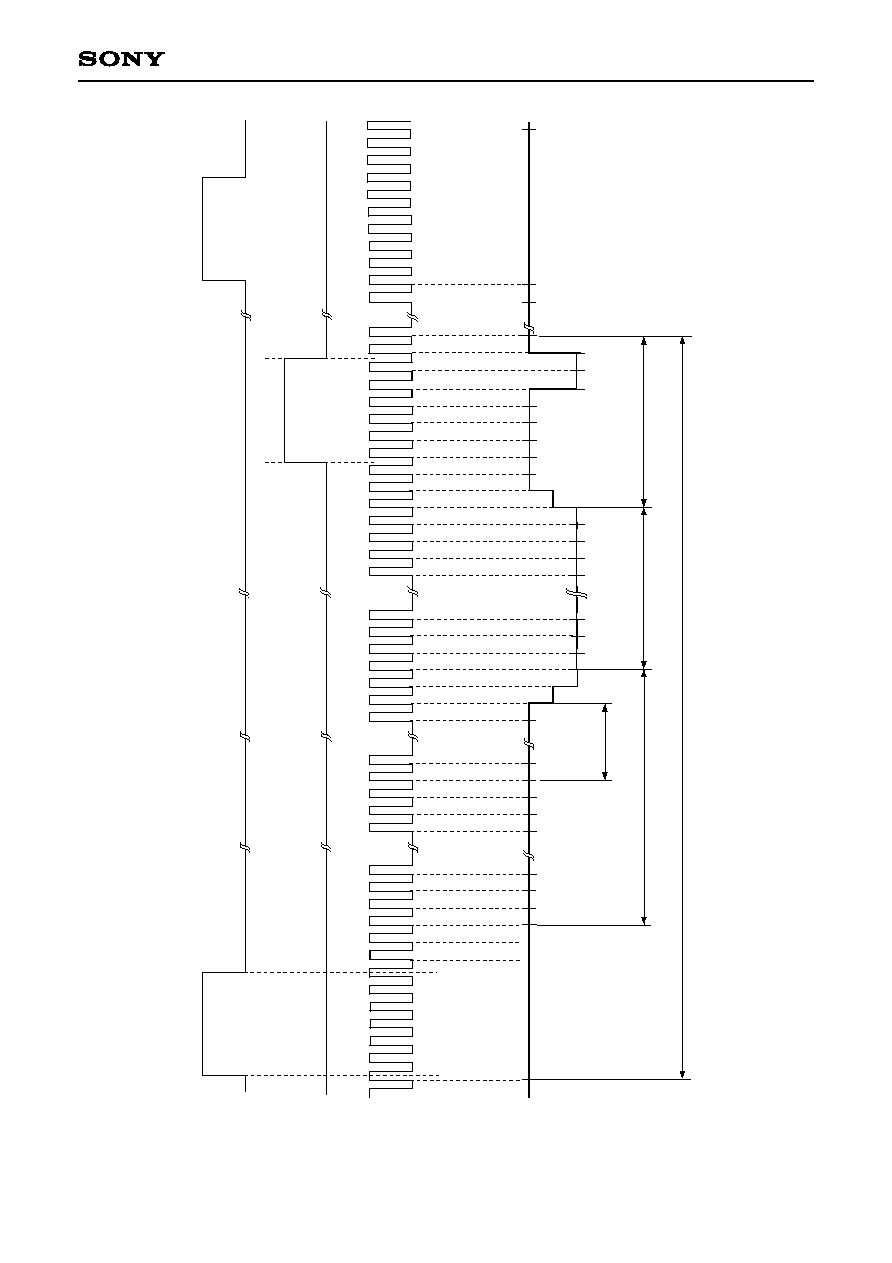
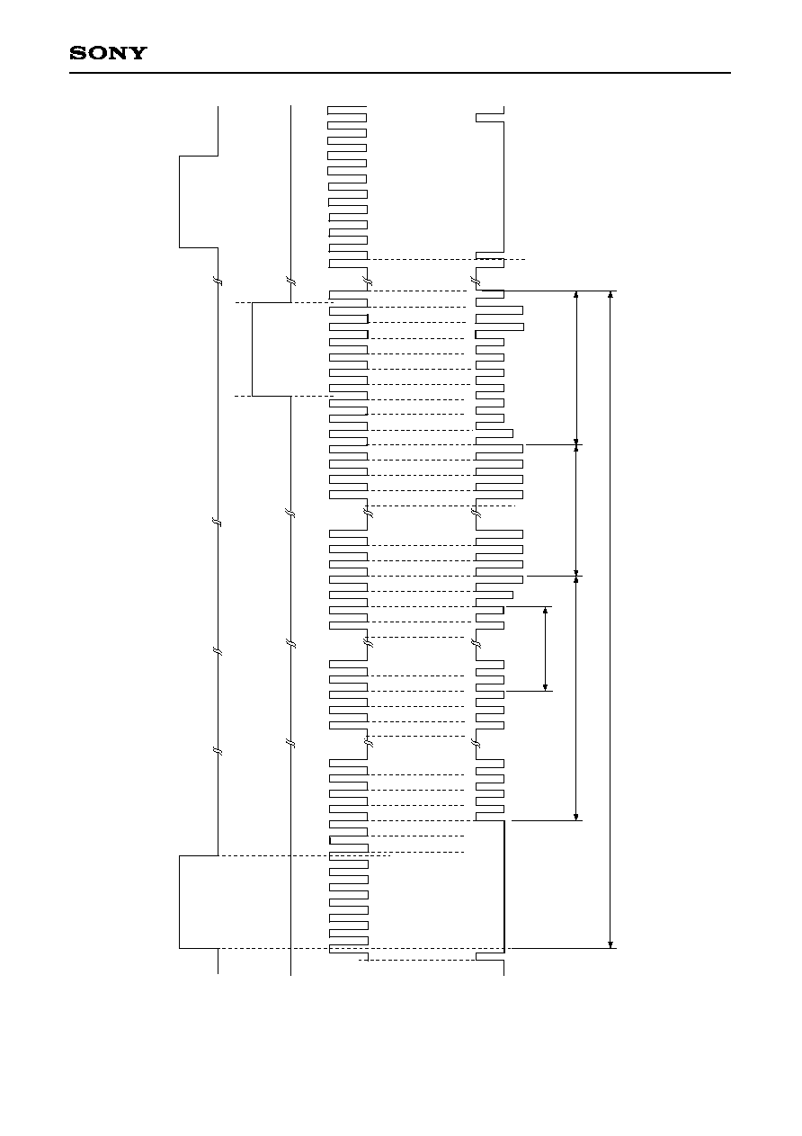
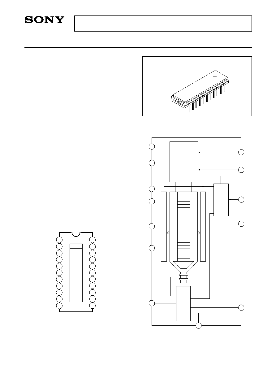
Pin Configuration (Top View)
Internal Structure
≠ 1 ≠
ILX526A
E97803-PS
3000-pixel CCD Linear Image Sensor (B/W)
Sony reserves the right to change products and specifications without prior notice. This information does not convey any license by
any implication or otherwise under any patents or other right. Application circuits shown, if any, are typical examples illustrating the
operation of the devices. Sony cannot assume responsibility for any problems arising out of the use of these circuits.
12
13
14
15
16
17
18
19
20
21
22
2
3
4
5
6
7
8
9
10
11
1
1
3000
S/HSW
GND
V
DD
NC
NC
NC
NC
NC
V
OUT
GND
V
DD
NC
T1
V
DD
GND
SHUT
ROG
NC
NC
NC
CLK
Vgg
Clock-drivers
CCD analog shift register
Readout gate
Readout gate
CCD analog shift register
Clock-drivers
Clock pulse
generator
Readout gate pulse
generator
Shutter pulse
generator
D24
D25
D54
D55
S1
S2
S3
S2999
S3000
D56
D65
1
21
22
14
13
9
8
7
6
2
10
12
20
Output Amplifier
S/H circuit
SHUT
ROG
CLK
T1
S/HSW
Vgg
GND
V
DD
V
DD
GND
V
DD
GND
V
OUT
22 pin DIP (Cer-DIP)
≠ 3 ≠
ILX526A
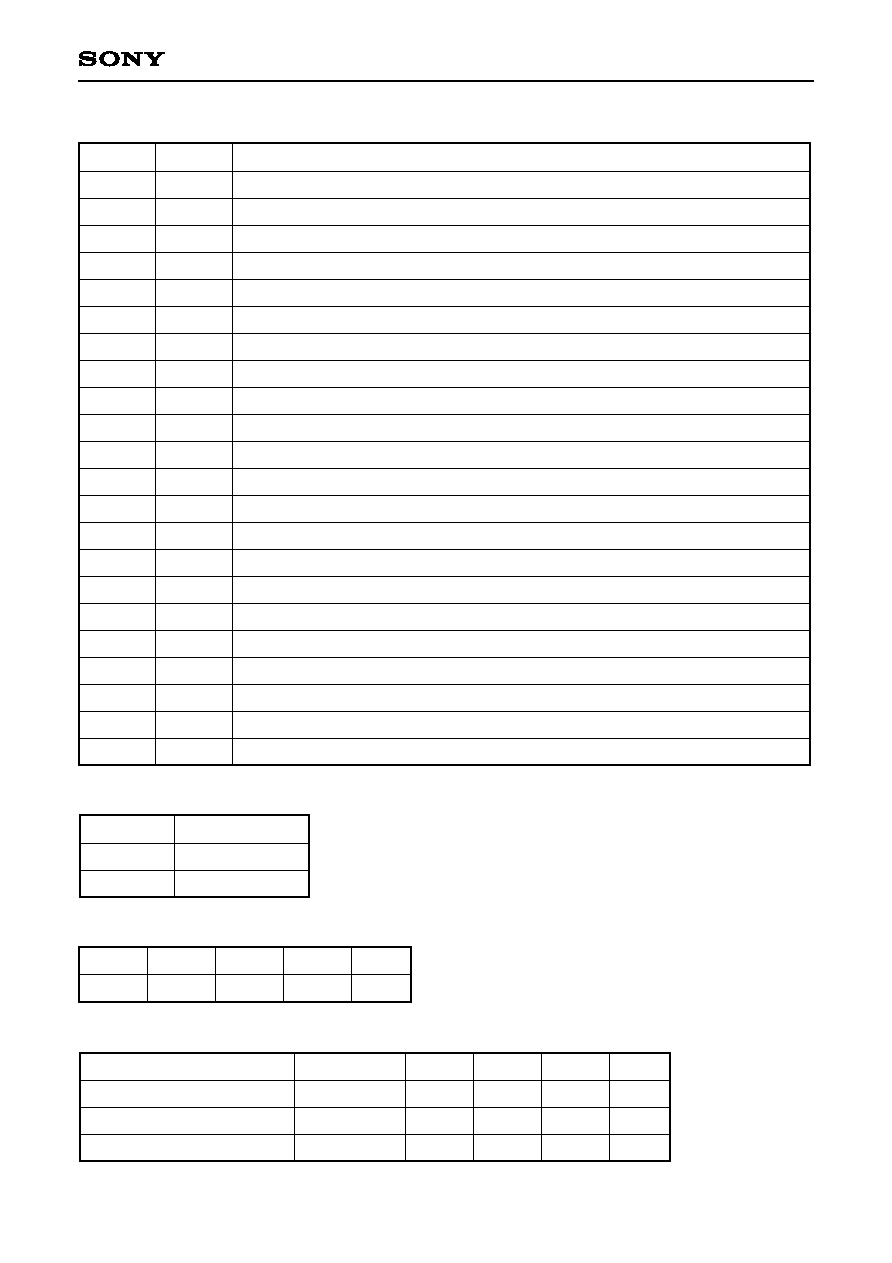
Electro-optical Characteristics (Note 1)
Ta = 25∞C, V
DD
= 5V, Clock frequency: 500kHz, Light source = 3200K,
IR cut filter: CM-500S (t = 1.0mm), Without S/H mode
Item
Symbol
Min.
Typ.
Max.
Unit
Remarks
Sensitivity 1
Sensitivity 2
Sensitivity nonuniformity
Saturation output voltage
Dark voltage average
Dark signal nonuniformity
Image lag
Dynamic range
Saturation exposure
5V current consumption
Total transfer efficiency
Output impedance
Offset level
R1
R2
PRNU
V
SAT
V
DRK
DSNU
IL
DR
SE
I
VDD
TTE
Z
O
V
OS
210
--
--
0.6
--
--
--
--
--
--
92.0
--
--
300
3700
5.0
0.8
2.5
5.0
5.0
320
0.003
7.0
97.0
250
2.5
390
--
10.0
--
6.0
12.0
--
--
--
17.0
--
--
--
V/(lx ∑ s)
V/(lx ∑ s)
%
V
mV
mV
%
--
lx ∑ s
mA
%
V
Note 2
Note 3
Note 4
--
Note 5
Note 6
Note 7
Note 8
Note 9
--
--
--
Note 10
Note)
1. In accordance with the given electrooptical characteristics, the even black level is defined as the average
value of D24, D26 to D52. The odd black level is defined as the average value of D25 , D27 to D53.
2. For the sensitivity test light is applied with a uniform intensity of illumination.
3. Light source: LED
= 660nm
4. PRNU is defined as indicated below. Ray incidence conditions are the same as for Note 2.
PRNU =
◊
100 [%]
Where the 3000 pixels are divided into blocks of even and odd pixels, respectively, the maximum output of
each block is set to V
MAX
, the minimum output to V
MIN
and the average output to V
AVE
.
5. Integration time is 10ms.
6. The difference between the maximum and average values of the dark output voltage is calculated for even
and odd respectively. Integration time is 10ms.
7. Typical value is used for clock pulse and readout pulse. V
OUT
= 500mV.
8.
DR =
When optical integration time is shorter, the dynamic range sets wider because dark voltage is in
proportion to optical integration time.
9.
SE =
10. Vos is defined as indicated below.
(V
MAX
≠ V
MIN
)/2
V
AVE
V
SAT
V
DRK
V
SAT
R1
V
OUT
GND
D52
D53
D51
D55
S1
D54
V
OS