 | –≠–ª–µ–∫—Ç—Ä–æ–Ω–Ω—ã–π –∫–æ–º–ø–æ–Ω–µ–Ω—Ç: ILX551A | –°–∫–∞—á–∞—Ç—å:  PDF PDF  ZIP ZIP |
2048-pixel CCD Linear Sensor (B/W)
Description
The ILX551A is a reduction type CCD linear sensor
designed for facsimile, image scanner and OCR use.
This sensor reads B4 size documents at a density of
200DPI (Dot Per Inch). A built-in timing generator
and clock-drivers ensure direct drive at 5V logic for
easy use.
Features
∑ Number of effective pixels: 2048 pixels
∑ Pixel size: 14µm
◊
14µm (14µm pitch)
∑ Built-in timing generator and clock-drivers
∑ Ultra low lag
∑ Maximum clock frequency: 5MHz
Absolute Maximum Ratings
∑ Supply voltage
V
DD1
11
V
V
DD2
6
V
∑ Operating temperature
≠10 to +55
∞C
∑ Storage temperature
≠30 to +80
∞C
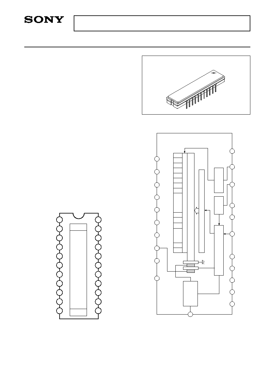
Pin Configuration (Top View)
Block Diagram
≠ 1 ≠
E00439-PS
Sony reserves the right to change products and specifications without prior notice. This information does not convey any license by
any implication or otherwise under any patents or other right. Application circuits shown, if any, are typical examples illustrating the
operation of the devices. Sony cannot assume responsibility for any problems arising out of the use of these circuits.
ILX551A
22 pin DIP (Cer-DIP)
22
20
17
16
15
14
13
12
10
9
11
4
21
19
5
8
7
6
3
2
1
V
OUT
Output amplifier
Sample-and-hold
circuit
V
DD2
18
NC
V
DD1
GND
NC
NC
NC
NC
GND
NC
V
DD2
ROG
SHSW
V
DD2
GND
CLK
V
DD2
NC
NC
NC
NC
Clock pulse generator
Sample-and-hold pulse generator
Mode
selector
Read out gate
pulse generator
Clock-drivers
CCD analog shift register
Read out gate
D14
D15
S1
D33
S2
S2047
S2048
D34
D35
D36
D37
D38
D39
1
22
V
OUT
2
NC
3
NC
4
SHSW
5
CLK
6
NC
7
NC
8
V
DD2
9
V
DD2
10
NC
11
21
20
19
18
17
16
15
14
13
12
ROG
V
DD2
V
DD2
V
DD1
GND
NC
GND
NC
NC
NC
NC
GND
1
2048
≠ 2 ≠
ILX551A
Unit
pF
pF
Max.
--
--
Typ.
10
10
Min.
--
--
Symbol
C
CLK
C
ROG
Item
Input capacity of
CLK pin
Input capacity of
ROG pin
Input Capacity of Pins
Item
Unit
V
V
Max.
9.5
5.25
Typ.
9.0
5.0
Min.
8.5
4.75
Item
V
DD1
V
DD2
Recommended Supply Voltage
Pin condition
Pin 4 SHSW
GND
V
DD2
Mode in use
S/H
Yes
No
Mode Description
Unit
V
V
Max.
5.5
0.5
Typ.
5.0
--
Min.
4.5
0.0
Input clock high level
Input clock low level
Recommended Input Pulse Voltage
Pin Description
Pin
No.
Symbol
Description
1
2
3
4
5
6
7
8
9
10
11
V
OUT
NC
NC
SHSW
CLK
NC
NC
V
DD2
V
DD2
NC
ROG
Signal output
NC
NC
with S/H
GND
Switch
without S/H
V
DD
2
Clock pulse
NC
NC
5V power supply
5V power supply
NC
Clock pulse
Pin
No.
Symbol
Description
12
13
14
15
16
17
18
19
20
21
22
GND
NC
NC
NC
NC
GND
NC
GND
V
DD1
V
DD2
V
DD2
GND
NC
NC
NC
NC
GND
NC
GND
9V power supply
5V power supply
5V power supply
Note) Rules for raising and lowering power supply voltage
To raise power supply voltage, first raise V
DD1
(9V) and then V
DD2
(5V).
To lower voltage, first lower V
DD2
(5V) and then V
DD1
(9V).
{
≠ 3 ≠
ILX551A
Unit
Remarks
Max.
50
8.0
--
2.0
3.0
--
--
--
8.0
5.0
--
--
--
Typ.
40
2.0
1.8
0.3
0.5
0.02
6000
0.045
4.0
1.8
97.0
600
4.0
Min.
30
--
1.5
--
--
--
--
--
--
--
92.0
--
--
Symbol
R
PRNU
V
SAT
V
DRK
DSNU
IL
DR
SE
I
VDD1
I
VDD2
TTE
Z
O
V
OS
Item
Electrooptical Characteristics
(Ta = 25∞C, V
DD1
= 9V, V
DD2
= 5V, Clock frequency = 1MHz, Light source = 3200K, IR cut filter: CM-500S (t = 1.0mm))
Notes)
1. For the sensitivity test light is applied with a uniform intensity of illumination.
2. PRNU is defined as indicated below. Ray incidence conditions are the same as for Note 1.
PRNU =
◊
100 [%]
The maximum output is set to V
MAX
, the minimum output to V
MIN
and the average output to V
AVE
.
3. Integration time is 10ms.
4. V
OUT
= 500mV
5. DR =
When optical accumulated time is shorter, the dynamic range gets wider because dark voltage is in
proportion to optical accumulated time.
6. SE =
7. Vos is defined as indicated below.
(V
MAX
≠ V
MIN
)/2
V
AVE
V
SAT
R
GND
OS
D31
D32
D33
S1
V
OS
,
V/(lx ∑ s)
%
V
mV
mV
%
--
lx ∑ s
mA
mA
%
V
Note 1
Note 2
--
Note 3
Note 3
Note 4
Note 5
Note 6
--
--
--
--
Note 7
Secsitivity
Sensitivity nonuniformity
Saturation output voltage
Dark voltage average
Dark signal nonuniformity
Image lag
Dynamic range
Saturation exposure
9V supply current
5V supply current
Total transfer efficiency
Output impedance
Offset level
V
SAT
V
DRK
≠ 4 ≠
ILX551A
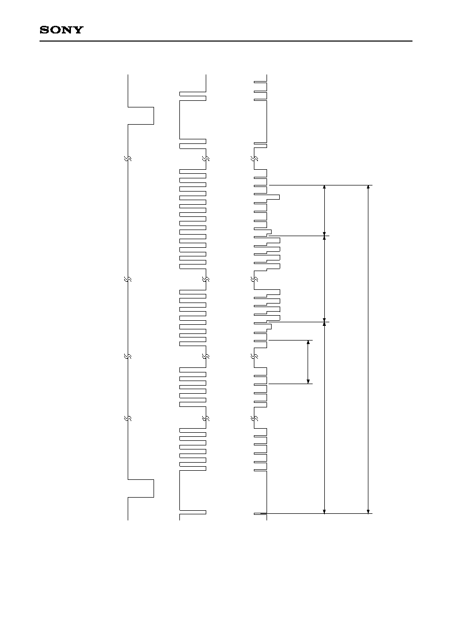
Fig. 1. Clock Timing Diagram (without S/H mode)
D
u
m
m
y
s
i
g
n
a
l
(
3
3
p
i
x
e
l
s
)
O
p
t
i
c
a
l
b
l
a
c
k
(
1
8
p
i
x
e
l
s
)
D
u
m
m
y
s
i
g
n
a
l
(
6
p
i
x
e
l
s
)
E
f
f
e
c
t
i
v
e
p
i
c
t
u
r
e
e
l
e
m
e
n
t
s
s
i
g
n
a
l
(
2
0
4
8
p
i
x
e
l
s
)
1
-
l
i
n
e
o
u
t
p
u
t
p
e
r
i
o
d
(
2
0
8
7
p
i
x
e
l
s
)
1
D2
D3
D4
D5
D6
D1
1
D1
2
D1
3
D1
4
D1
5
D3
1
D3
2
D3
3
S1
S2
S3
S4
S2
04
5
S2
04
6
S2
04
7
S2
04
8
D3
4
D3
5
D3
6
S3
7
S3
8
D3
9
2
3
4
20
87
1
2
5
R
O
G
C
L
K
V
O
U
T
0
5
0
≠ 5 ≠
ILX551A
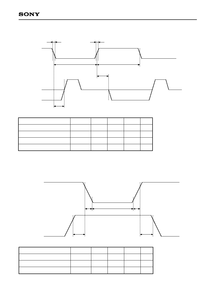
Fig. 2.
CLK, V
OUT
Timing
,,
,
,,
CLK
t3
t4
t2
t1
t5
t6
V
OUT
Item
CLK pulse rise/fall time
CLK pulse duty
1
CLK ≠ V
OUT
1
CLK ≠ V
OUT
2
Symbol
t1, t2
--
t5
t6
Min.
0
40
50
30
Typ.
10
50
80
75
Max.
--
60
110
120
Unit
ns
%
ns
ns
1
100
◊
t3/(t3 + t4)
Fig. 3.
ROG,
CLK Timing
ROG
CLK
t7
t11
t8
t10
t9
Item
ROG,
CLK pulse timing
ROG pulse rise/fall time
ROG pulse period
Symbol
t7, t11
t8, t10
t9
Min.
500
0
500
Typ.
1000
10
1000
Max.
--
--
--
Unit
ns
ns
ns