 | –≠–ª–µ–∫—Ç—Ä–æ–Ω–Ω—ã–π –∫–æ–º–ø–æ–Ω–µ–Ω—Ç: LCX012BL | –°–∫–∞—á–∞—Ç—å:  PDF PDF  ZIP ZIP |
≠ 1 ≠
LCX012BL
E96512-ST
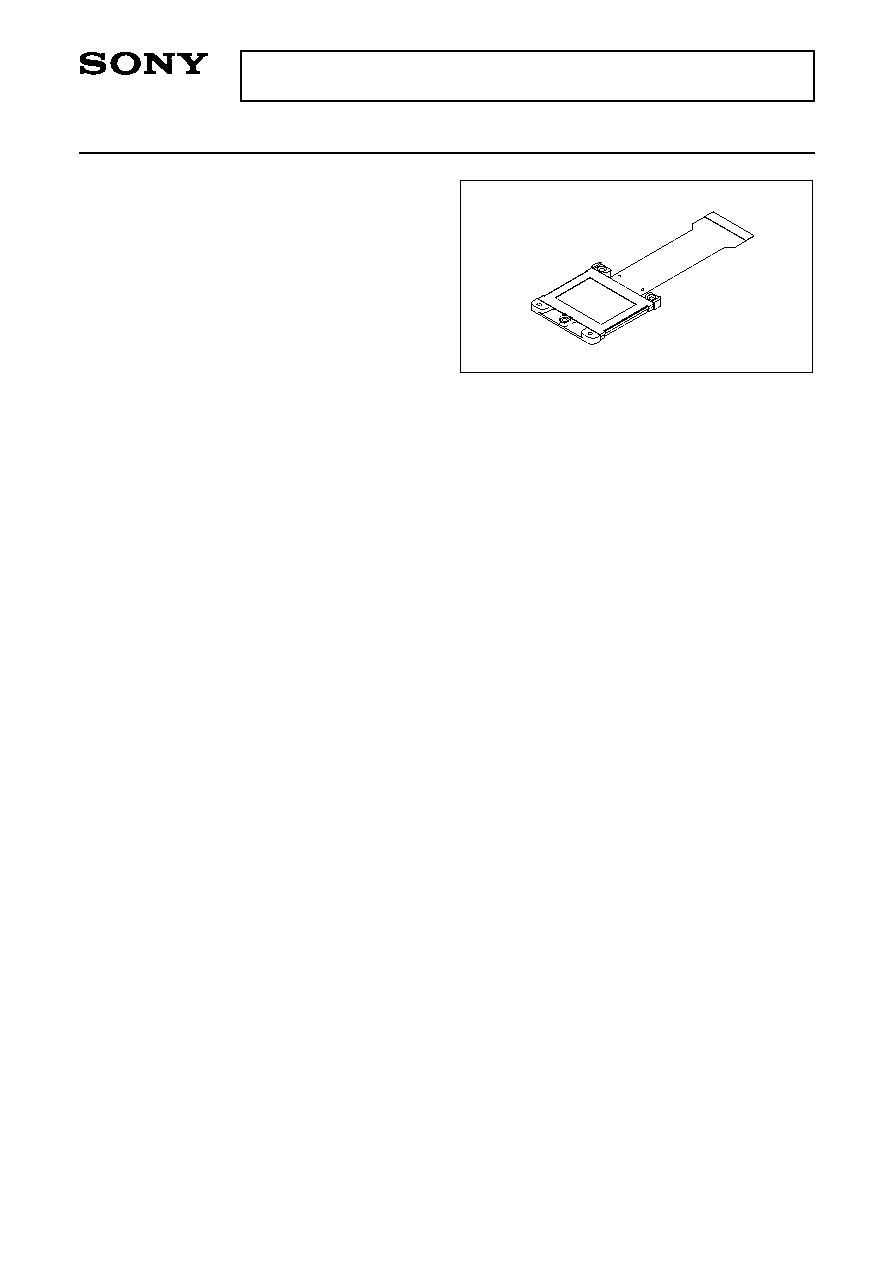
3.3cm (1.3-inch) Black-and-White LCD Panel
Description
The LCX012BL is a 3.3cm diagonal active matrix
TFT-LCD panel addressed by polycrystalline silicon
super thin film transistors with built-in peripheral
driving circuit. Use of three panels in combination
with the LCX012BL provides a full-color represen-
tation. The striped arrangement suitable for data
projectors is capable of displaying fine text and
vertical lines.
The adoption of advanced on-chip black matrix
realizes high picture quality without cross talk by
incorporating high luminance screen and cross talk
free circuit.
This panel has a polysilicon TFT high-speed
scanner and built-in function to display images
up/down and/or right/left inverse. The built-in 5V
interface circuit leads to lower voltage of timing and
control signals.
Using Sony's timing generator "CXD2442Q" sends
timing signal necessary for LCD panel drive by
identificating computer supporting VGA automati-
cally, and supports double-speed processed
NTSC/PAL.
Features
∑ The number of active dots: 312,000 (1.3-inch; 3.3cm in diagonal)
∑ Accepts the computer requirements of VGA platform (640 x 480)
∑ High optical transmittance: 25% (typ.)
∑ Supports NTSC/PAL by processing the video signal at double speed
∑ Built-in cross talk free circuit
∑ High contrast ratio with normally white mode: 250 (typ.)
∑ Built-in H and V drivers (built-in input level conversion circuit, 5V driving possible)
∑ Up/down and/or right/left inverse display function
Element Structure
∑ Dots: 644 (H)
◊
484 (V) = 311,696
∑ Built-in peripheral driver using polycrystalline silicon super thin film transistors.
Applications
∑ Liquid crystal data projectors
∑ Liquid crystal projectors, etc.
Sony reserves the right to change products and specifications without prior notice. This information does not convey any license by
any implication or otherwise under any patents or other right. Application circuits shown, if any, are typical examples illustrating the
operation of the devices. Sony cannot assume responsibility for any problems arising out of the use of these circuits.
≠ 2 ≠
LCX012BL
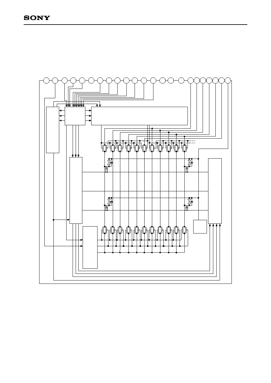
Block Diagram
1
2
11
12
13
17
10
19
18
21
20
15
9
22
14
8
7
6
5
4
3
23
16
Input Signal
Level
Shifter
H Shift Register (Bidrectional Scanning)
Up/Down or Right/Left
Inversion
V Shift Register
(Bidrectional Scanning)
Uniformity Improvement
Signal Control Circuit
COM
PAD
V Shift Register
(Bidrectional Scanning)
COM
SIG6
SIG5
SIG4
SIG3
SIG2
SIG1
Vss
VV
DD
HV
DD
CLR
ENB
DWN
PCG
VCK
VST
RGT
NC
HCK2
HCK1
HST
PSIG
NC
≠ 3 ≠
LCX012BL
Absolute Maximum Ratings (V
SS
= 0V)
∑ H driver supply voltage
HV
DD
≠1.0 to +20
V
∑ V driver supply voltage
VV
DD
≠1.0 to +20
V
∑ Common pad voltage
COM
≠1.0 to +17
V
∑ H shift register input pin voltage
HST, HCK1, HCK2,
≠1.0 to +17
V
RGT
∑ V shift register input pin voltage
VST, VCK, PCG,
≠1.0 to +17
V
CLR, ENB, DWN
∑ Video signal input pin voltage
SIG1, SIG2, SIG3, SIG4,
≠1.0 to +15
V
SIG5, SIG6, PSIG
∑ Operating temperature
Topr
≠10 to +70
∞C
∑ Storage temperature
Tstg
≠30 to +85
∞C
Operating Conditions (V
SS
= 0V)
Supply voltage
HV
DD
15.5 ±0.5 V
VV
DD
15.5 ±0.5 V
Input pulse voltage (Vp-p of all input pins except video signal and uniformity improvement signal input pins)
Vin
5.0 ±0.5
V
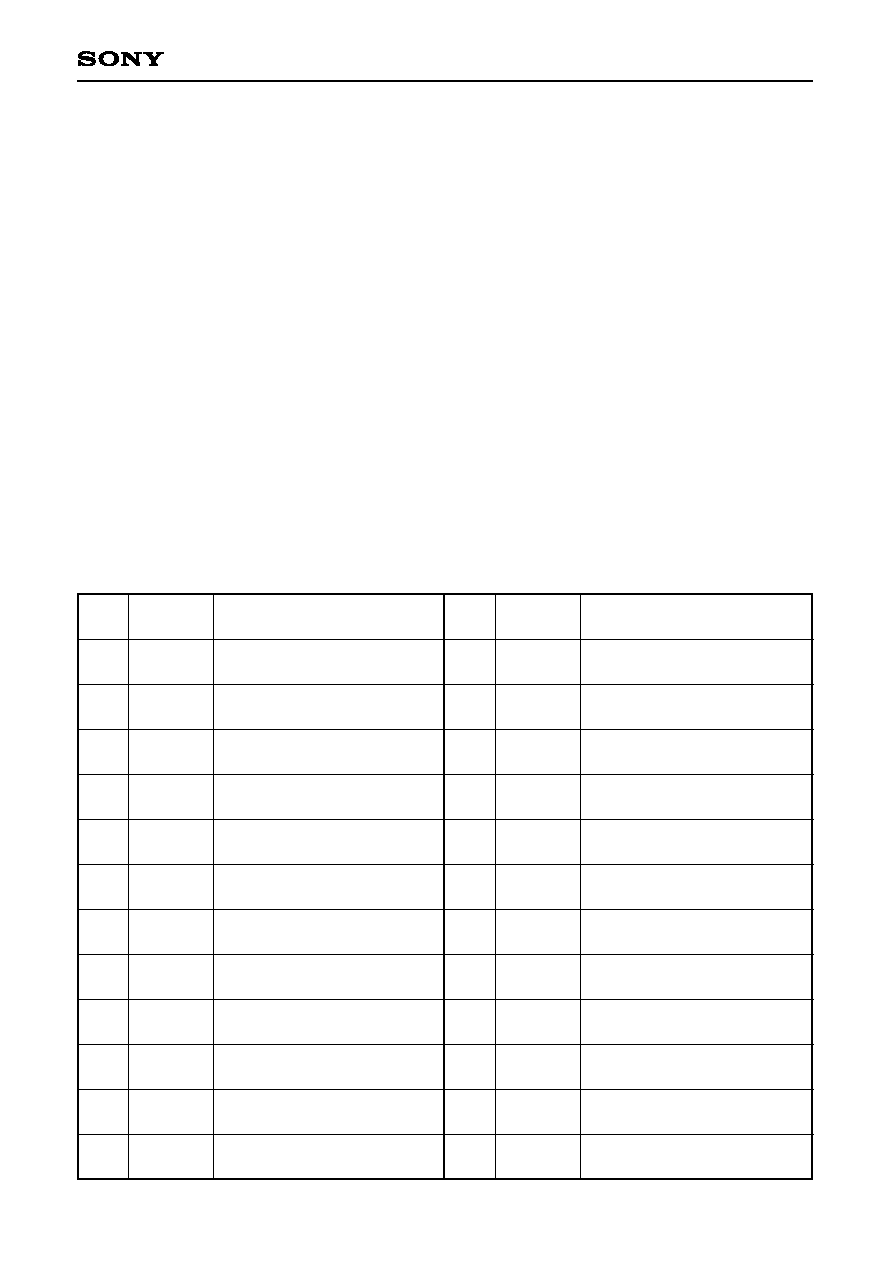
Pin Description
Pin
No.
1
2
3
4
5
6
7
8
9
10
11
12
NC
PSIG
SIG6
SIG5
SIG4
SIG3
SIG2
SIG1
HV
DD
RGT
HST
HCK1
13
14
15
16
17
18
19
20
21
22
23
24
HCK2
V
SS
CLR
ENB
NC
VCK
VST
DWN
PCG
VV
DD
COM
TEST
Clock pulse for H shift register
drive
GND (H, V drivers)
Improvement pulse (1) for
uniformity
Enable pulse for gate selection
NC; Open
Clock pulse for V shift register
drive
Start pulse for V shift register
drive
Drive direction pulse for V shift
register (H: normal, L: reverse)
Improvement pulse (2) for
uniformity
Power supply for V driver
Common voltage of panel
Test; Open
Symbol
Description
Pin
No.
Symbol
Description
NC; Open
Uniformity improvement signal
Video signal 6 to panel
Video signal 5 to panel
Video signal 4 to panel
Video signal 3 to panel
Video signal 2 to panel
Video signal 1 to panel
Power supply for H driver
Driver direction pulse for H shift
register (H: normal, L: reverse)
Start pulse for H shift register
drive
Clock pulse for H shift register
drive
≠ 4 ≠
LCX012BL
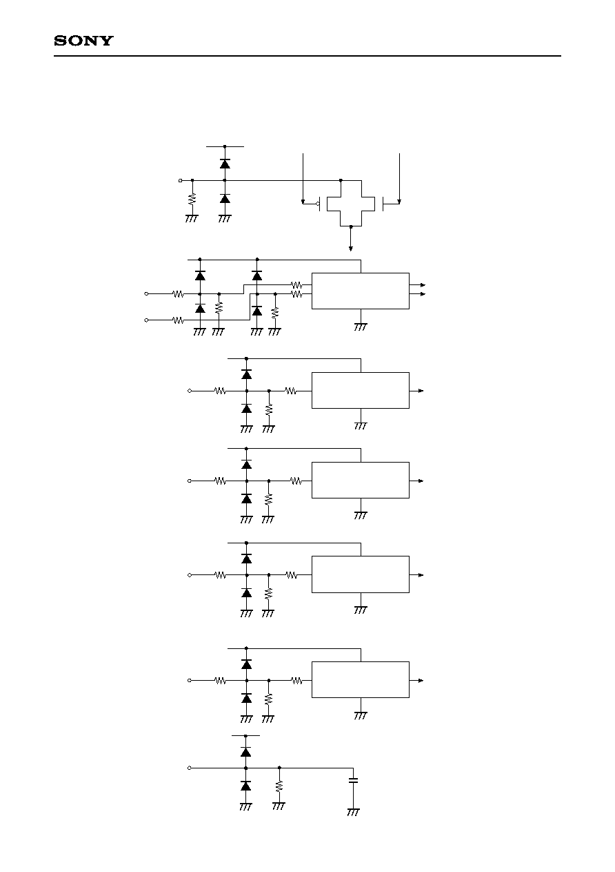
Input Equivalent Circuit
To prevent static charges, protective diodes are provided for each pin except the power supply. In addition,
protective resistors are added to all pins except video signal input. All pins are connected to V
SS
with a high
resistance of 1M
(typ.). The equivalent circuit of each input pin is shown below: (The resistor value: typ.)
Input
LC
Level conversion circuit
(single-phase input)
2.5k
2.5k
VV
DD
Input
Level conversion circuit
(single-phase input)
250
250
HV
DD
Input
Level conversion circuit
(single-phase input)
2.5k
2.5k
HV
DD
Input
HV
DD
250
250
250
250
Level conversion circuit
(2-phase input)
Input
HV
DD
Signal line
(1) SIG1, SIG2, SIG3, SIG4, SIG5, SIG6, PSIG
(2) HCK1, HCK2
(3) RGT
(4) HST
(5) PCG, VCK
(6) VST, CLR, ENB, DWN
(7) COM
1M
Input
1M
1M
1M
Level conversion circuit
(single-phase input)
250
250
VV
DD
Input
1M
1M
1M
VV
DD
1M

≠ 5 ≠
LCX012BL
Input Signals
1. Input signal voltage conditions
(V
SS
= 0V)
Item
H driver input voltage
(Low)
(High)
(Low)
(High)
VHIL
VHIH
VVIL
VVIH
VVC
Vsig
Vcom
Vpsig
≠0.5
4.5
≠0.5
4.5
6.8
VVC ≠ 4.5
VVC ≠ 0.5
VVC ± 3.3
0.0
5.0
0.0
5.0
7.0
7.0
VVC ≠ 0.4
VVC ± 3.5
0.4
5.5
0.4
5.5
7.2
VVC + 4.5
VVC ≠ 0.3
VVC ± 3.7
V
V
V
V
V
V
V
V
V driver input voltage
Video signal center voltage
Video signal input range
1
(SIG1 to 6)
Common voltage of panel
2
Uniformity improvement signal
input voltage (PSIG)
3
Symbol
Min.
Typ.
Max.
Unit
1
input signal shall be symmetrical to VVC.
2
The typical value of the common pad voltage may lower its suitable voltage according to the set
construction to use. In this case, use the voltage of which has maximum contrast as typical value. When the
typical value is lowered, the maximum and minimum values may lower.
3
Input a uniformity improvement signal PSIG in the same polarity with video signals SIG1 to 6 and which is
symmetrical to VVC. Also, the rising and falling of PSIG are synchronized with the rising of PCG pulse, and
the rise time trPSIG and fall time tfPSIG are suppressed within 800ns (as shown in a diagram below).
Input waveform of uniformity improvement signal PSIG
Level Conversion Circuit
The LCX012BL has a built-in level conversion circuit in the clock input unit on the panel. The input signal level
increases to HV
DD
or VV
DD
. The V
CC
of external ICs are applicable to 5 ± 0.5V.
trPSIG
tfPSIG
VVC
PSIG
PCG
90%
10%