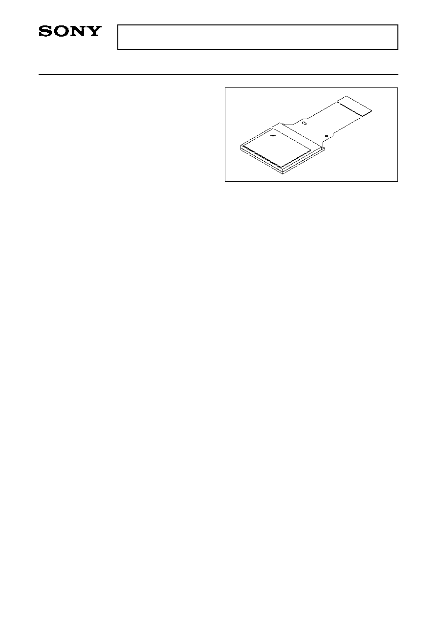
1.8cm (0.7-inch) Color LCD Panel
Description
The LCX020BK is a 1.8cm diagonal active matrix
TFT-LCD panel addressed by polycrystalline silicon
super thin film transistors with built-in peripheral driving
circuit. This panel provides full-color representation.
RGB dots are arranged in a striped pattern optimum
for data applications and capable of displaying fine
text and vertical lines.
The adoption of an advanced on-chip black matrix
realizes a high luminance screen, and high picture
quality is possible with built-in cross talk free and
ghost free circuits.
This panel has a polysilicon TFT high-speed
scanner and built-in function to display images
up/down and/or right/left inverse. In addition, the
built-in 5V interface circuit leads to lower voltage of
timing and control signals.
The panel contains a display area varying circuit
which supports Macintosh16
1
/SVGA/VGA/PC98
2
data signals by changing the display area according
to the type of input signal. In addition, double-speed
processed NTSC/PAL/WIDE can also be supported.
1
"Macintosh" is a trademark of Apple Company Inc.
2
"PC98" is a trademark of NEC.
Features
� Number of active dots: 1,557,000, 1.8cm (0.7-inch) in diagonal
� Supports Macintosh16 (832
�
624), SVGA (800
�
600), VGA (640
�
480) and PC98 (640
�
400) display
� Supports NTSC (640
�
480), PAL (762
�
572) and WIDE (832
�
480) display by processing the video signal
at double speed
� High optical transmittance: 1% (typ.)
� Built-in cross talk free circuit
� High contrast ratio with normally white mode: 70 (typ.)
� Built-in H and V drivers (built-in input level conversion circuit, 5V driving possible)
� Up/down and/or right/left inverse display function
Element Structure
� Dots: 2496 (H)
�
624 (V) = 1,557,504
� Built-in peripheral driving circuit using polycrystalline silicon super thin film transistors
Applications
� Liquid crystal EVFs for personal PCs/DVDs
� Small monitors, etc.
� 1 �
E99210-PS
Sony reserves the right to change products and specifications without prior notice. This information does not convey any license by
any implication or otherwise under any patents or other right. Application circuits shown, if any, are typical examples illustrating the
operation of the devices. Sony cannot assume responsibility for any problems arising out of the use of these circuits.
LCX020BK
� 2 �
LCX020BK
H
S
h
i
f
t
R
e
g
i
s
t
e
r
(
B
i
d
i
r
e
c
t
i
o
n
a
l
S
c
a
n
n
i
n
g
)
Up
/D
ow
n a
nd
/o
r R
ig
ht/
Le
ft
In
ve
rs
io
n C
on
tro
l C
irc
uit
V S
hif
t R
eg
is
te
r (
Bid
ire
cti
on
al
Sc
an
nin
g)
C
O
M
P
a
d
CO
M
SIG
R6
SIG
R5
SIG
R4
SIG
R3
SIG
R2
SIG
R1
V
SS
VV
DD
HV
DD
MO
DE
1
EN
B
DW
N
PC
G
VC
K
VS
T
RG
T
BL
K
HC
K2
HC
K1
HS
T
PS
IG
B
B
l
a
c
k
F
r
a
m
e
C
o
n
t
r
o
l
C
i
r
c
u
i
t
Bla
ck
F
ra
me
C
on
tro
l C
irc
uit
MO
DE
2
MO
DE
3
I
n
p
u
t
S
i
g
n
a
l
L
e
v
e
l
S
h
i
f
t
e
r
C
i
r
c
u
i
t
Pre
ch
arg
e
Co
ntr
ol
Cir
cu
it
1
5
6
7
8
9
1
0
1
1
1
2
1
3
1
4
1
5
1
6
1
7
1
8
1
9
2
0
2
1
2
2
2
3
3
1
4
2
3
2
4
2
5
2
6
2
7
2
8
2
9
3
0
3
2
3
3
3
4
3
5
3
6
3
7
3
8
SIG
G6
SIG
G5
SIG
G4
SIG
G3
SIG
G2
SIG
G1
SIG
B6
SIG
B5
SIG
B4
SIG
B3
SIG
B2
SIG
B1
PS
IG
R
PS
IG
G
V S
hif
t R
eg
is
te
r (
Bid
ire
cti
on
al
Sc
an
nin
g)
Bla
ck
F
ra
me
C
on
tro
l C
irc
uit
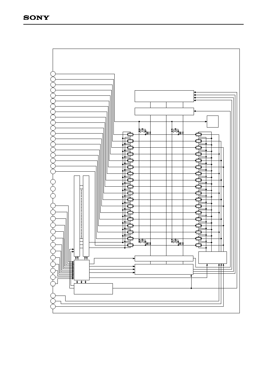
Block Diagram
The Block Diagram of the panel is shown below.
� 3 �
LCX020BK
Absolute Maximum Ratings (Vss = 0V)
� H driver supply voltage
HV
DD
�1.0 to +20
V
� V driver supply voltage
VV
DD
�1.0 to +20
V
� Common pad voltage
COM
�1.0 to +17
V
� H shift register input pin voltage
HST, HCK1, HCK2,
�1.0 to +17
V
RGT
� V shift register input pin voltage
VST, VCK, PCG,
�1.0 to +17
V
BLK, ENB, DWN
MODE1, MODE2, MODE3
� Video signal input pin voltage
SIGR1 to SIGR6,
�1.0 to +15
V
SIGG1 to SIGG6,
SIGB1 to SIGB6,
PSIGR, PSIGG, PSIGB
� Operating temperature
Topr
�10 to +70
�C
� Storage temperature
Tstg
�30 to +85
�C
Operating Conditions (Vss = 0V)
� Supply voltage
HV
DD
15.5 � 0.3V
VV
DD
15.5 � 0.3V
� Input pulse voltage (Vp-p of all input pins except video signal and uniformity improvement signal input pins)
Vin
5.0 � 0.5V
Pin Description
Pin
No.
1
2
3
4
5
6
7
8
9
10
11
12
13
14
COM
PSIGR
PSIGG
PSIGB
SIGR1
SIGR2
SIGR3
SIGR4
SIGR5
SIGR6
SIGG1
SIGG2
SIGG3
SIGG4
Common voltage of panel
Uniformity improvement signal input (R)
Uniformity improvement signal input (G)
Uniformity improvement signal input (B)
Video signal input to panel (R-1)
Video signal input to panel (R-2)
Video signal input to panel (R-3)
Video signal input to panel (R-4)
Video signal input to panel (R-5)
Video signal input to panel (R-6)
Video signal input to panel (G-1)
Video signal input to panel (G-2)
Video signal input to panel (G-3)
Video signal input to panel (G-4)
Symbol
Description
� 4 �
LCX020BK
15
16
17
18
19
20
21
22
23
24
25
26
27
28
29
30
31
32
33
34
35
36
37
38
39
SIGG5
SIGG6
SIGB1
SIGB2
SIGB3
SIGB4
SIGB5
SIGB6
HV
DD
RGT
MODE3
MODE2
MODE1
HST
HCK1
HCK2
V
SS
BLK
ENB
VCK
VST
DWN
PCG
VV
DD
SOUT
Video signal input to panel (G-5)
Video signal input to panel (G-6)
Video signal input to panel (B-1)
Video signal input to panel (B-2)
Video signal input to panel (B-3)
Video signal input to panel (B-4)
Video signal input to panel (B-5)
Video signal input to panel (B-6)
Power supply input for H driver
Drive direction input for H shift register (H: normal, L: reverse)
Display area switching 3 input
Display area switching 2 input
Display area switching 1 input
Start pulse input for H shift register drive
Clock pulse input for H shift register drive
Clock pulse input for H shift register drive
GND (H, V drivers)
Black frame display pulse input
Gate selection pulse enable input
Clock pulse input for V shift register drive
Start pulse input for V shift register drive
Drive direction input for V shift register (H: normal, L: reverse)
Uniformity improvement pulse input
Power supply input for V driver
H and V shift register drive checking (Test pin; no connection.)
Pin
No.
Symbol
Description
� 5 �
LCX020BK
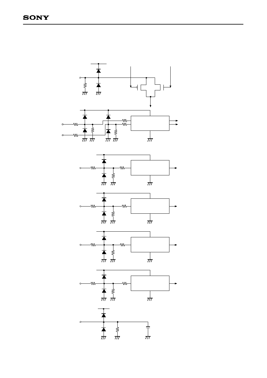
Input Equivalent Circuits
To prevent static charges, protective diodes are provided for each pin except the power supplies. In addition,
protective resistors are added to all pins except video signal inputs. All pins are connected to Vss with a high
resistance of 1M
(typ.). The equivalent circuit of each input pin is shown below: (Resistor value: typ.)
Input
LC
Level conversion circuit
(single-phase input)
2.5k
2.5k
VV
DD
Input
Level conversion circuit
(single-phase input)
250
250
HV
DD
Input
Level conversion circuit
(single-phase input)
2.5k
2.5k
HV
DD
Input
Input
HV
DD
Signal line
(1) SIGR1 to SIGR6, SIGG1 to SIGG6, SIGB1 to SIGB6, PSIGR, PSIGG, PSIGB
(2) HCK1, HCK2
(3) RGT, MODE1, MODE2, MODE3
(4) HST
(5) PCG, VCK
(6) VST, BLK, ENB, DWN
(7) COM
1M
1M
Level conversion circuit
(single-phase input)
250
250
VV
DD
Input
1MW
1M
1M
VV
DD
Input
HV
DD
250
250
250
250
Level conversion circuit
(2-phase input)
1M
1M
1M