 | –≠–ª–µ–∫—Ç—Ä–æ–Ω–Ω—ã–π –∫–æ–º–ø–æ–Ω–µ–Ω—Ç: LCX028BLT | –°–∫–∞—á–∞—Ç—å:  PDF PDF  ZIP ZIP |
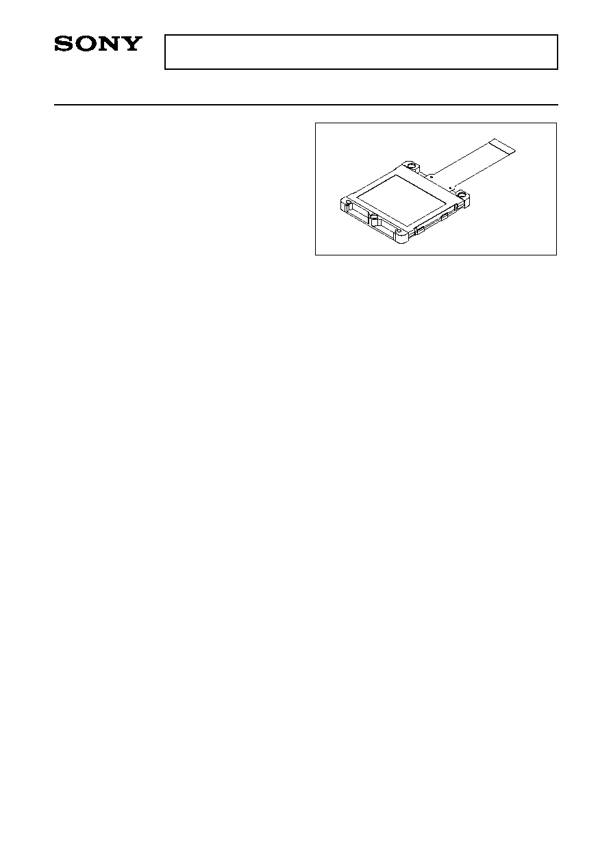
LCX028BLT
4.6cm (1.8-inch) Black-and-White LCD Panel
Description
The LCX028BLT is a 4.6cm diagonal active matrix
TFT-LCD panel addressed by polycrystalline silicon
super thin film transistors with a built-in peripheral
driving circuit. Use of three LCX028BLT panels
provides a full-color representation. The striped
arrangement suitable for data projectors is capable
of displaying fine text and vertical lines.
The adoption of an advanced on-chip black matrix
realizes a high luminance screen. And cross talk free
circuit and ghost free circuit contribute to high
picture quality.
This panel has a polysilicon TFT high-speed
scanner and built-in function to display images
up/down and/or right/left inverse. The built-in 5V
interface circuit leads to lower voltage of timing and
control signals.
The panel contains an active area variable circuit
which supports 4:3 and 16:9 data signals by changing
the active area according to the type of input signal.
Features
∑ Number of active dots: 1,310,720 (1.8-inch, 4.6cm in diagonal)
∑ 4:3 and 16:9 aspect-ratio switching function
4:3 (1280 (H)
◊
960 (V))
16:9 (1280 (H)
◊
720 (V))
∑ High optical transmittance: 20% (typ.)
∑ Built-in cross talk free circuit and ghost free circuit
∑ High contrast ratio with normally white mode: 300 (typ.)
∑ Built-in H and V drivers (built-in input level conversion circuit, 5V driving possible)
∑ Up/down and/or right/left inverse display function
∑ Antidust glass package
∑ Microlens used
Element Structure
∑ Dots: 1280 (H)
◊
1024 (V) = 1,310,720
∑ Built-in peripheral driver using polycrystalline silicon super thin film transistors
Applications
∑ Liquid crystal data projectors
∑ Liquid crystal multimedia projectors
∑ Liquid crystal rear-projector TVs, etc.
≠ 1 ≠
E00637A15
Sony reserves the right to change products and specifications without prior notice. This information does not convey any license by
any implication or otherwise under any patents or other right. Application circuits shown, if any, are typical examples illustrating the
operation of the devices. Sony cannot assume responsibility for any problems arising out of the use of these circuits.
The company's name and product's name in this data sheet is a trademark or a registered trademark of each company.
≠ 2 ≠
LCX028BLT
18
COM
VSIG6
VSIG5
VSIG4
VSIG3
VSIG2
VSIG1
Vss
VV
DD
HV
DD
ENB
DWN
PCG
VCK
VST
RGT
BLK
HCK2
HCK1
HST
V
SS
G
PSIG
17
20
19
22
23
16
2
24
VB1
VB2
25
29
26
28
15
30
27
COMR
9
12
11
10
8
7
4
3
5
13
6
14
VSIG7
VSIG8
VSIG9
VSIG10
VSIG11
VSIG12
1
21
COML
32
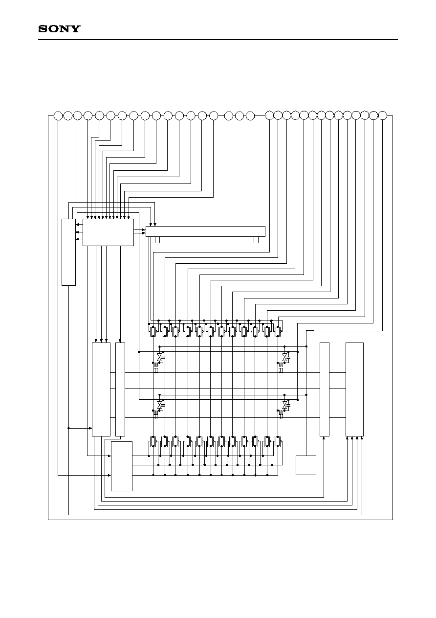
H Shift Register (Bidirectional Scanning)
Up/Down and/or Right/Left
Inversion Control Circuit
V Shift Register
(Bidirectional Scanning)
Precharge Control
Circuit
COM
PAD
V Shift Register
(Bidirectional Scanning)
Black Frame Control Circuit
Black Frame Control Circuit
Input Signal
Level Shifter
Circuit
31
Block Diagram

≠ 3 ≠
LCX028BLT
Absolute Maximum Ratings (V
SS
= 0V)
∑ H driver supply voltage
HV
DD
≠1.0 to +20
V
∑ V driver supply voltage
VV
DD
≠1.0 to +20
V
∑ Common pad voltage
COM, COML, COMR
≠1.0 to +17
V
∑ H shift register input pin voltage HST, HCK1, HCK2,
≠1.0 to +17
V
RGT
∑ V shift register input pin voltage
VST, VCK, PCG,
≠1.0 to +17
V
BLK, ENB, DWN
VB1, VB2
∑ Video signal input pin voltage
SIG1 to 12, PSIG
≠1.0 to +15
V
∑ Operating temperature
Topr
≠10 to +70
∞C
∑ Storage temperature
Tstg
≠30 to +85
∞C
Panel temperature inside the antidust glass
Operating Conditions (V
SS
= 0V)
∑ Supply voltage
HV
DD
15.5 ± 0.5V
VV
DD
15.5 ± 0.5V
∑ Input pulse voltage (Vp-p of all input pins except video signal and uniformity improvement signal input pins)
≠ 4 ≠
LCX028BLT
Pin Description
Pin
No.
1
2
3
4
5
6
7
8
9
10
11
12
13
14
15
16
17
18
19
20
21
22
23
24
25
26
27
28
29
30
31
32
PSIG
COMR
VSIG1
VSIG2
VSIG3
VSIG4
VSIG5
VSIG6
VSIG7
VSIG8
VSIG9
VSIG10
VSIG11
VSIG12
HV
DD
RGT
HST
HCK1
HCK2
V
SS
COML
BLK
ENB
VCK
VST
DWN
VB1
VB2
PCG
VV
DD
V
SS
G
COM
Symbol
Description
Uniformity improvement signal
Voltage for right CS (storage capacity) electrode line
Video signal 1 to panel
Video signal 2 to panel
Video signal 3 to panel
Video signal 4 to panel
Video signal 5 to panel
Video signal 6 to panel
Video signal 7 to panel
Video signal 8 to panel
Video signal 9 to panel
Video signal 10 to panel
Video signal 11 to panel
Video signal 12 to panel
Power supply for H driver
Drive direction pulse for H shift register (H: nomal, L: reverse)
Start pulse for H shift register drive
Clock pulse for H shift register drive 1
Clock pulse for H shift register drive 2
GND (H, V drivers)
Voltage for left CS (storage capacity) electrode line
Black Frame display pulse
Enable pulse for gate selection
Clock pulse for V shift register drive
Start pulse for V shift register drive
Drive direction pulse for V shift register (H: nomal, L: reverse)
Display area switching 1
Display area switching 2
Improvement pulse for uniformity
Power supply for V driver
GND for V gate
Common voltage of panel
≠ 5 ≠
LCX028BLT
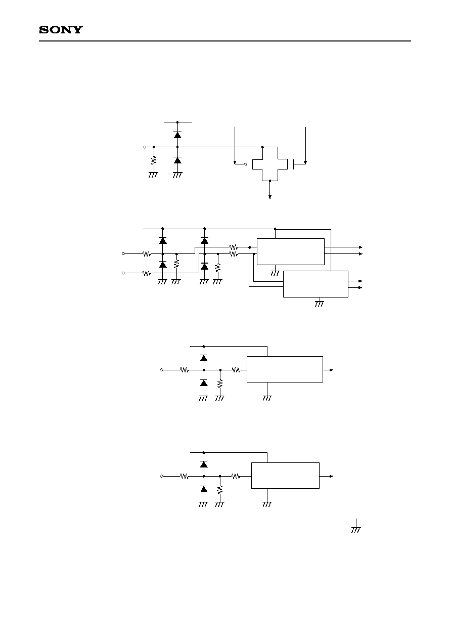
Input Equivalent Circuit
To prevent static charges, protective diodes are provided for each pin except the power supplies. In addition,
protective resistors are added to all pins except the video signal inputs. All pins are connected to V
SS
with a
high resistor of 1M
(typ.). The equivalent circuit of each input pin is shown below: (Resistance value: typ.)
Input
HV
DD
Signal line
1M
(1) VSIG1 to VSIG12, PSIG
HV
DD
250
250
250
250
Level conversion circuit
(2-phase input)
Input
1M
1
Level conversion circuit
(2-phase input)
(2) HCK1,HCK2
Level conversion circuit
(single-phase input)
2.5k
2.5k
HV
DD
Input
1M
(3) RGT
Level conversion circuit
(single-phase input)
250
250
HV
DD
Input
1M
(4) HST
are all Vss