 | –≠–ª–µ–∫—Ç—Ä–æ–Ω–Ω—ã–π –∫–æ–º–ø–æ–Ω–µ–Ω—Ç: MCX18N00B | –°–∫–∞—á–∞—Ç—å:  PDF PDF  ZIP ZIP |
Peripheral ICs
∑ EVR: MB88347 (Fujitsu Limited.)
∑ EEPROM: AK6420 (Asahi Kasei Microsystems
Co., Ltd.)
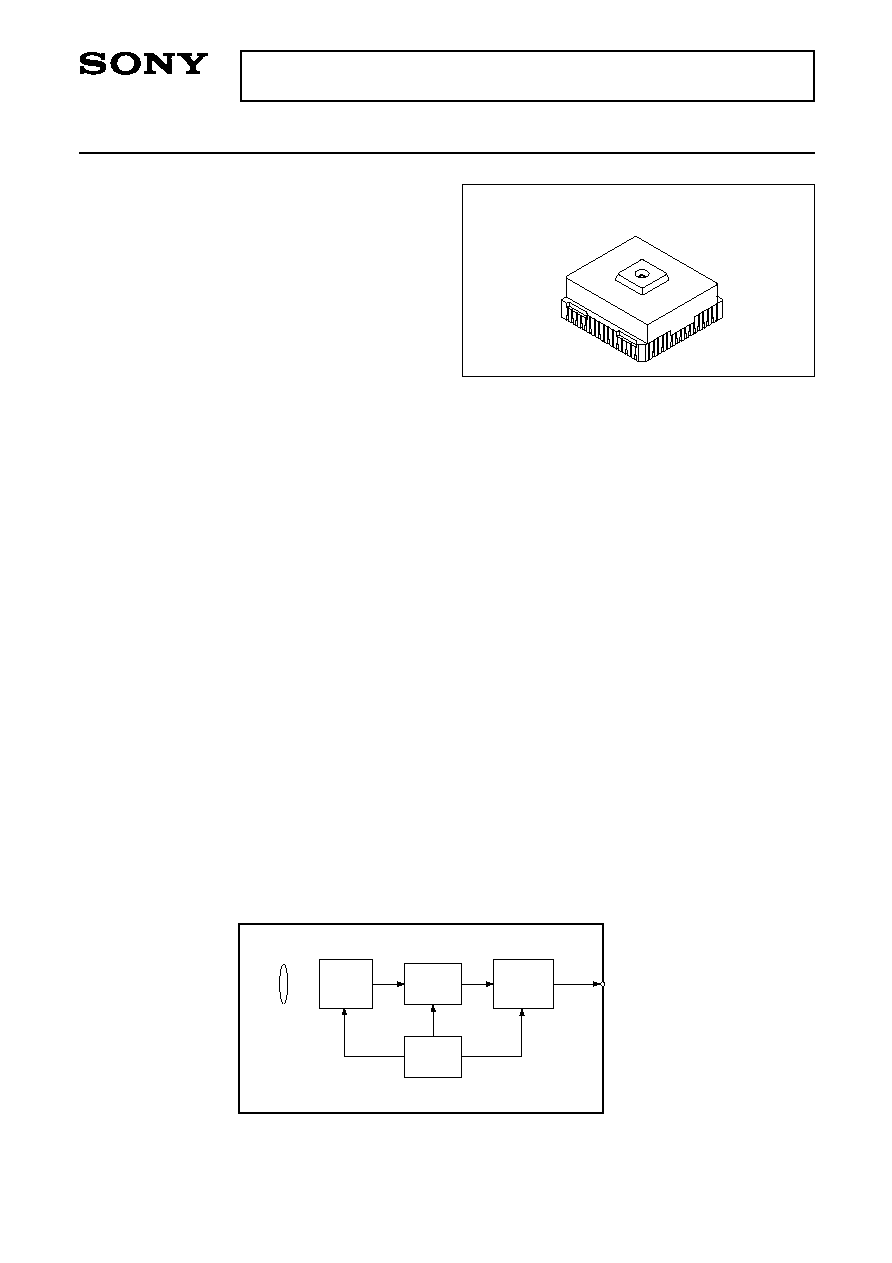
Description
The micro unit CCD is a CCD color camera unit
with built-in CCD image sensor, drive system IC,
sample-and-hold IC, signal processor IC and lens
system.
Features
∑ Ultra-compact size:
MCX18N00A
18.3mm
◊
18.3mm
◊
8.4mm
MCX18N00B
18.3mm
◊
18.3mm
◊
9.6mm
∑ Y/C analog output
∑ Employs a Type 1/5,
180,000-pixel color CCD image sensor
∑ Equipped with a fixed focus lens:
MCX18N00A
F2.8/f = 2.9mm
MCX18N00B
F2.8/f = 4.0mm
Applications
∑ TV conference cameras
∑ Image input cameras
Absolute Maximum Ratings
∑ Supply voltage
V
H
+18
V
DV
DD
1, DV
DD
2, AV
DD
6
+7.0
V
AV
DD
1, AV
DD
2, AV
DD
3
+7.0
V
AV
DD
4, AV
DD
5
+7.0
V
V
CC
+14.0
V
V
L
≠17.5
V
∑ Input voltage
V
I
≠0.5 to DV
DD
+ 0.5
V
∑ Operating temperature
Topr
0 to +40
∞C
∑ Storage temperature
Tstg
≠30 to +80
∞C
Recommended Operating Conditions
∑ Supply voltage
V
H
14.25 to 15.75
V
DV
DD
1, DV
DD
2, AV
DD
6
3.0 to 3.6
V
AV
DD
1, AV
DD
2, AV
DD
3
4.75 to 5.25
V
AV
DD
4, AV
DD
5
4.5 to 5.5
V
V
CC
4.5 to 5.25
V
V
L
≠8.5 to ≠7.5
V
∑ Input voltage
V
DCIN
1.0 to 4.5
V
∑ Operating temperature
Topr
0 to +40
∞C
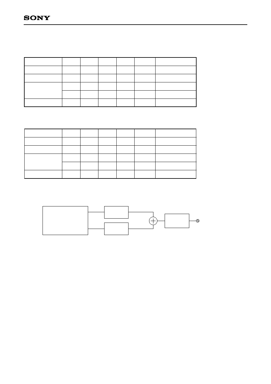
Block Diagram
≠ 1 ≠
MCX18N00A/MCX18N00B
E97432B9X
Micro Unit CCD
Sony reserves the right to change products and specifications without prior notice. This information does not convey any license by
any implication or otherwise under any patents or other right. Application circuits shown, if any, are typical examples illustrating the
operation of the devices. Sony cannot assume responsibility for any problems arising out of the use of these circuits.
64 pin QFN (Ceramic)
Lens
Y/C
CCD
Image
Sensor
S/H
Digital
Signal
Process
Timing
Generator
≠ 2 ≠
MCX18N00A/MCX18N00B
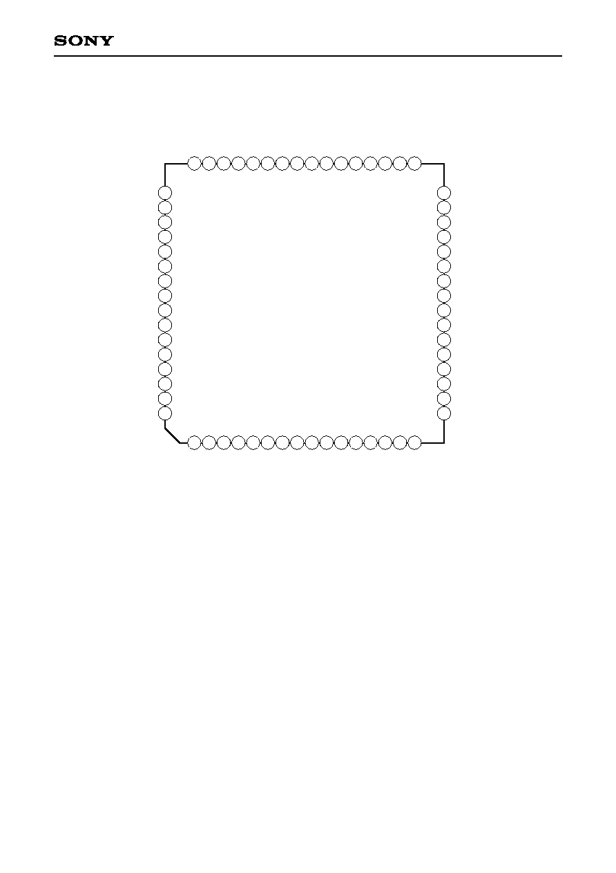
Pin Configuration
40
39
38
37
36
35
34
31
32
33
41
42
43
44
45
46
47
48
49
50
51
52
53
54
55
56
57
58
59
60
63
64
61
62
2
3
4
5
6
7
8
9 10 11 12 13 14 15 16 17 18 19 20 21 22 23 24
25
26
27
28
29
30
1
D
V
D
D
2
A
G
N
D
V
H
A
G
N
D
A
V
D
D
4
V
C
C
T
E
S
T
S
U
B
I
N
A
G
C
C
O
N
T
O
F
F
S
E
T
A
V
D
D
1
A
V
D
D
2
A
V
D
D
3
D
C
I
N
D
C
O
U
T
S
U
B
O
U
T
I
R
E
F
C
V
R
E
F
C
V
B
C
C
C
D
O
U
T
D
G
N
D
D
G
N
D
D
G
N
D
H
D
V
D
P
C
O
M
P
A
G
N
D
4
F
S
C
O
4
F
S
C
I
A
V
D
D
6
X
C
L
R
S
C
K
SI
SO
CASI
CSROM
RESETTG
DGND
OSCI
OSCO
CK
DV
DD
1
XCS
CASCK
CASO
CSEVR
DGND
VL
VGC
AV
DD
5
IOC
IOY
VGY
IREFY
VREFY
VBY
DGND
DGND
DGND
SHOUT
SHIN
AGND
AGND
SIFSEL
≠ 3 ≠
MCX18N00A/MCX18N00B
Pin Description
Pin
No.
Symbol
I/O
Description
1
2
3
4
5
6
7
8
9
10
11
12
13
14
15
16
17
18
19
20
21
22
23
24
25
26
27
28
29
30
31
32
33
34
35
DGND
DGND
DGND
SHOUT
SHIN
AGND
AGND
SIFSEL
DV
DD
2
AGND
VH
AGND
AV
DD
4
V
CC
TEST
SUBIN
AGCCONT
OFFSET
AV
DD
1
AV
DD
2
AV
DD
3
DCIN
DCOUT
SUBOUT
VL
DGND
CSEVR
CASO
CASCK
XCS
DV
DD
1
CK
OSCO
OSCI
DGND
--
--
--
O
I
--
I
I
--
--
--
--
--
--
I
I
I
I
--
--
--
I
O
O
--
--
O
O
O
I
--
I
O
I
--
Digital GND
Digital GND
Digital GND
Sample-and-hold output. Connect directly to Pin 5.
Sample-and-hold input.
Analog GND
Analog GND
Serial communication mode selection: Microcomputer (low)/RS232C (high).
+3.3V power supply for signal processing system.
Analog GND
+15V power supply for CCD image sensor drive.
Analog GND
+5V power supply for A/D converter.
+5V power supply for sample-and-hold.
Test pin. Connect to V
CC
.
CCD image sensor SUB voltage input.
AGC control.
OFFSET control.
+5V power supply for sample-and-hold pulse.
+5V power supply for RG pulse.
+5V power supply for H pulse.
DC amplifier input.
DC amplifier output.
SUB pulse output.
≠8V power supply for CCD image sensor drive.
Digital GND
EVR chip select.
Serial communication data output for peripheral ICs (EVR, EEPROM).
Serial communication clock output for peripheral ICs (EVR, EEPROM).
Switched by the SIFSEL setting.
Chip select during microcomputer mode.
Baud rate setting (4800bps (low)/9600bps (high)) during RS232C mode.
+3.3V power supply for timing generator.
27MHz clock input.
27MHz oscillator output.
27MHz oscillator input.
Digital GND
≠ 4 ≠
MCX18N00A/MCX18N00B
36
37
38
39
40
41
42
43
44
45
46
47
48
49
50
51
52
53
54
55
56
57
58
59
60
61
62
63
64
RESETTG
CSROM
CASI
SO
SI
SCK
XCLR
AV
DD
6
4FSCI
4FSCO
AGND
PCOMP
VD
HD
DGND
DGND
DGND
CCDOUT
VBC
VREFC
IREFC
VGC
AV
DD
5
IOC
IOY
VGY
IREFY
VREFY
VBY
I
O
I
O
I
I
I
--
I
O
--
O
O
O
--
--
--
O
I
--
O
O
I
Reset pin (active low) with pull-up resistor for timing generator.
EEPROM chip select.
Serial communication data input for peripheral ICs (EVR, EEPROM).
Serial communication data output.
Serial communication data input.
Serial communication clock input.
Initialization pin (active low). EEPROM re-read.
+3.3V power supply for 4fsc oscillator.
4fsc oscillator input.
4fsc oscillator output.
Analog GND
Phase comparison output for PLL lock.
Vertical sync output.
Horizontal sync output.
Digital GND
Digital GND
Digital GND
CCD image sensor buffer output.
D/A converter peripheral circuit connection pins for chroma signal.
+5V power supply for D/A converter.
Chroma signal output.
Luminance signal output.
D/A converter peripheral circuit connection pins for luminance signal.
Pin
No.
Symbol
I/O
Description
≠ 5 ≠
MCX18N00A/MCX18N00B
Item
Electrical Characteristics
DC Characteristics
Symbol
Unit
Min.
Typ.
Max.
Pins
Conditions
Input voltage 1
Input voltage 2
Input voltage 3
Input voltage 4
Input voltage 5
DV
DD
1
DV
DD
2
AV
DD
1
AV
DD
2
AV
DD
3
AV
DD
4
AV
DD
5
AV
DD
6
V
CC
V
H
V
L
I
DD
1
I
DD
2
IA
DD
1
IA
DD
2
IA
DD
3
IA
DD
4
IA
DD
5
IA
DD
6
I
CC
I
H
I
L
V
T+
V
T≠
V
IH
1
V
IL
1
V
DCIN
V
SUB
V
IH
2
V
IL
2
5
,
7
1
,
6
DCIN
SUBIN
4FSCI
A/D input amplitude = 2Vp-p
D/A output amplitude = 2Vp-p
DV
DD
1 = 3.3V
DV
DD
2 = 3.3V
AV
DD
1 = 5.0V
AV
DD
2 = 5.0V
AV
DD
3 = 5.0V
AV
DD
4 = 5.0V
AV
DD
5 = 5.0V
AV
DD
6 = 3.3V
V
CC
= 5.0V
V
H
= 15.0V
V
L
= ≠8.0V
V
V
V
V
V
V
V
V
V
V
V
mA
mA
mA
mA
mA
mA
mA
mA
mA
mA
mA
V
V
V
V
V
3.0
3.0
4.75
4.75
4.75
4.5
4.5
3.0
4.5
14.25
≠8.5
DV
DD
2
◊
0.8
DV
DD
1
◊
0.7
1.0
Display
value ≠ 0.1
AV
DD
4
◊
0.7
3.3
3.3
5.00
5.00
5.00
5.0
5.0
3.3
5.0
15.00
≠8.0
7.2
36
3.1
1.0
4.9
15
24
1.0
54
6.9
1.4
Display
value
3.6
3.6
5.25
5.25
5.25
5.5
5.5
3.6
5.25
15.75
≠7.5
DV
DD
2
◊
0.2
DV
DD
1
◊
0.3
4.5
Display
value + 0.1
AV
DD
4
◊
0.3
Operating
current
Supply voltage
≠ 6 ≠
MCX18N00A/MCX18N00B
2
3
4
SUBOUT
4FSCO
OSC
4FSC
OSC
SIFSEL
7
5
TEST
6
4FSCI
Item
Symbol
Unit
Min.
Typ.
Max.
Pins
Conditions
Output voltage 1
Output voltage 2
Output voltage 3
Output voltage 4
Output voltage 5
Hysteresis 1
Hysteresis 2
Threshold value 1
Threshold value 2
Threshold value 3
Feedback resistance 1
Feedback resistance 2
Input amplitude
Pull-up resistance
DC amplifier gain
Input leak current 1
Input leak current 2
V
OH
1
V
OL
1
V
OH
2
V
OL
2
V
OH
3
V
OL
3
V
OH
4
V
OL
4
V
OH
5
V
OL
5
V
TH
1
V
TH
2
V
TH
3
RFE1
RFE2
RPU
G
I
I
3
I
I
2
I
OH
1 = ≠1.2mA
I
OL
1 = 2.4mA
I
OH
2 = ≠2.4mA
I
OL
2 = 4.8mA
I
OH
3 = ≠8mA
I
OL
3 = 8mA
I
OH
4 = ≠4mA
I
OL
4 = 5.4mA
I
OH
5 = ≠3mA
I
OL
5 = 3mA
OSCI = DV
DD
1 or GND
4FSCI = AV
DD
4 or GND
50MHz sine wave
VIN = DV
DD
2
VIN = GND or DV
DD
2
V
V
V
V
V
V
V
V
V
V
Vp-p
µA
µA
DV
DD
2 ≠ 0.8
DV
DD
2 ≠ 0.8
DV
DD
1/2
V
H
≠ 0.25
AV
DD
4/2
500k
250k
0.5
50k
12
≠10
0.5
0.6
1.35
DV
DD
1/2
AV
DD
4/2
2M
1M
100k
4.4
30
0.4
0.4
DV
DD
1/2
V
L
+ 0.25
AV
DD
4/2
5M
2.5M
150k
75
10
1
RESETTG
2
CSEVR, CSROM, SO, PCOMP, VD, HD
3
CASO, CASCK
4
OSCO
5
XCS, SI, SCK, XCLR, CASI
6
OSCI, CK
7
SIFSEL
1
5
≠ 7 ≠
MCX18N00A/MCX18N00B
Note) VSUB display value
The VSUB display value is displayed by a code on the rear surface of the MUC.
Symbol
--
Actual voltage (V) 5.00
=
5.25
0
5.50
1
5.75
2
6.00
3
6.25
4
6.50
6
6.75
7
7.00
8
7.25
9
7.50
A
7.75
C
8.00
D
8.25
Symbol
E
Actual voltage (V) 8.50
f
8.75
G
9.00
h
9.25
J
9.50
K
9.75
L
10.00
m
10.25
N
10.50
P
10.75
R
11.00
S
11.25
U
11.50
V
11.75
Symbol
W
Actual voltage (V) 12.00
X
12.25
Y
12.50
Z
12.75
Minimum low interval
Minimum low interval
SCK input pulse width (high interval)
SCK input pulse width (low interval)
XCS input setup time, activated by the falling edge
of SCK
XCS input hold time, activated by the rising edge of
SCK
SI input setup time, activated by the rising edge of
SCK
SI input hold time, activated by the rising edge of
SCK
SO output transition time (Hi-Z
Data active),
activated by the falling edge of XCS
SO transition time (Data active
Hi-Z),
activated by the rising edge of XCS
SO output delay time, activated by the falling edge
of SCK
T
W
CLR
T
W
RST
T
WH
SCK
T
WL
SCK
T
SU
XCS
T
H
XCS
T
SU
SI
T
H
SI
T
ZD
SO
T
DZ
SO
T
PD
SO
500
35
430
430
430
640
140
140
70
70
70
--
--
--
--
--
--
--
--
--
--
--
--
--
--
--
--
--
--
--
200
200
240
ns
ns
ns
ns
ns
ns
ns
ns
ns
ns
ns
Serial
communication
XCLR
RESETTG
Classification
Item
Symbol
Min.
Typ.
Max. Unit
T
SU
XCS
T
H
XCS
T
WL
SCK
T
WH
SCK
T
ZD
SO
T
PD
SO
T
DZ
SO
DATA
DATA
DATA
DATA
DATA
T
H
SI
DATA
T
SU
SI
SI
SO
SCK
XCS
AC Characteristics
≠ 8 ≠
MCX18N00A/MCX18N00B
Image Sensor Characteristics
(Ta = 25∞C)
Item
Sensitivity
Saturation signal
Smear
Dark signal
Dark signal shading
S
Ysat
Sm
Ydt
Ydt
285
700
360
0.007
0.012
2
1
mV
mV
%
mV
mV
1
2
3
4
5
Center of screen
Ta = 60∞C, center of screen
Ta = 60∞C
Ta = 60∞C
Symbol
Min.
Typ.
Max.
Unit
Measure-
ment
method
Remarks
Measurement System
C.D.S
LPF1
AMP
CCD OUT
Y signal output
(3dB down 4MHz)
[
Y]
[
A]
Note) Adjust the amplifier gain so that the gain between [
A] and [
Y] equals 1.
Micro unit CCD

≠ 9 ≠
MCX18N00A/MCX18N00B
Image Sensor Characteristics Measurement Method
Measurement conditions
(1) In the following measurements, each supply voltage is at the typical values.
(2) In the following measurements, spot blemishes are excluded and, unless otherwise specified, the optical
black level (OB) is used as the reference for the signal output, which is taken as the value of Y signal
output of the measurement system.
Definition of Standard Imaging Conditions
1) Standard imaging condition
I
: Use a pattern box (luminance 706cd/m2, color temperature of 3200K halogen
source) as a subject. (Pattern for evaluation is not applicable.) Use a ND2 filter and image at F5.6 or
equivalent. The luminous intensity to the sensor receiving surface at this point is defined as the standard
sensitivity testing luminous intensity.
2) Standard imaging condition
II
: Image a light source with a uniformity of brightness within 2% at all angles
(color temperature of 3200K).
1. Sensitivity
Set to standard imaging condition
I
. After selecting the electronic shutter mode with a shutter speed of
1/250s, measure the Y signal (Ys) at the center of the screen and substitute the values into the following
formula.
S = Ys
◊
[mV]
2. Saturation signal
Set to standard imaging condition
II
. After adjusting the luminous intensity to 10 times the intensity applying
with an average value of Y signal output, 200mV, measure the minimum value of the Y signal.
3. Smear
Set to standard imaging condition
II
. With using ND2 filter and the lens diaphragm at F5.6 or equivalent,
adjust the luminous intensity to 500 times the intensity applying with an average value of Y signal output,
200mV. When the readout clock is stopped and the charge drain is executed by the electronic shutter at
the respective H blankings, measure the maximum value YSm [mV] of the Y signal output, and substitute
the values into the following formula.
4. Dark signal
Measure the average value of the Y signal output (Ydt [mV]) with the device ambient temperature of 60∞C
and the device in the light-obstructed state, using the horizontal idle transfer level as a reference.
5. Dark signal shading
After measuring 4, measure the maximum (Ydmax [mV]) and minimum (Ydmin [mV]) values of the Y signal
output, and substitute the values into the following formula.
Ydt = Ydmax ≠ Ydmin [mV]
Sm =
◊
100 [%] (1/10V method conversion value)
◊
◊
200
YSm
500
1
10
1
60
250
≠ 10 ≠
MCX18N00A/MCX18N00B
Measurement System
VIDEO OUT
Micro unit CCD
AMP
LPF
BPF
IOY
IOC
Optical Characteristics
MCX18N00A
Item
Focus length
Aperture
Shading
Resolution
f
F
SH
SV
R
2.9
2.8
220
50
25
%
%
TV lines
Horizontal
Vertical
Center of screen
Symbol
Min.
Typ.
Max.
Unit
Remarks
MCX18N00B
Item
Focus length
Aperture
Shading
Resolution
f
F
SH
SV
R
4.0
2.8
220
30
15
%
%
TV lines
Horizontal
Vertical
Center of screen
Symbol
Min.
Typ.
Max.
Unit
Remarks
≠ 11 ≠
MCX18N00A/MCX18N00B
Communication Code Table
1
1
1
1
1
1
1
1
1
1
1
1
1
1
1
1
2
2
2
2
2
2
2
2
2
2
2
2
2
2
3
3
3
3
3
3
1
2
3
3
4
4
5
6
7
8
9
10
11
12
13
14
1
2
3
4
5
6
7
7
7
7
8
9
10
11
1
2
3
4
5
6
0 to 7
0 to 7
0 to 3
4 to 7
0 to 3
4 to 7
0 to 7
0 to 7
0 to 7
0 to 7
0 to 7
0 to 7
0 to 7
0 to 7
0 to 7
0 to 7
0 to 7
0 to 7
0 to 7
0 to 7
0 to 7
0 to 7
0 to 3
4
5
6 to 7
0 to 7
0 to 7
0 to 7
0 to 7
0 to 7
0 to 7
0 to 7
0 to 7
0 to 7
0 to 7
YDLY
RMATY
RMATC
BMATY
BMATC
YGAIN
RBQUAD
CONGAIN
CONHUE
RYGAIN
BYGAIN
RYHUE
BYHUE
SHOFST
Setup level
Luminance signal delay adjustment
Matrix coefficient
Matrix coefficient
Matrix coefficient
Matrix coefficient
Luminance signal gain
Linear matrix quadrant control
Linear matrix gain
Linear matrix hue
Linear matrix coefficient
Linear matrix coefficient
Linear matrix coefficient
Linear matrix coefficient
Sample-and-hold output offset
00
01
D
6
E
4
24
34
0B
32
F8
32
D3
0C
00
00
86
AA
26
84
04
FC
F
1
1
0
20
11
D0
F8
00
00
00
3D
89
00
00
01
0
6
E
8
24
34
0B
2A
12
3E
CA
0C
00
FF
86
AA
26
84
04
FC
--
--
--
--
Adjustment value
Adjustment value
Adjustment value
Adjustment value
00
00
00
3D
89
00
01
02
03
03
04
04
05
06
07
08
09
0A
0B
0C
0D
0E
0F
10
11
12
13
14
4F, 51, 53, 55
50, 52, 54, 56
57, 59, 5B, 5D
58, 5A, 5C, 5E
15
16
17
18
19
1A
Cate-
gory
Byte
Bit
Symbol
Description
EEPROM
Address (H)
Recommended
value (H)
Initial
value (H)
≠ 12 ≠
MCX18N00A/MCX18N00B
3
4
4
4
4
5
5
5
5
5
5
5
5
5
5
6
6
6
6
6
7
7
7
7
7
8
8
8
8
8
8
8
8
8
8
7
1
2
3
4
1
2
3
3
3
3
4
5
6
7
1
2
3
4
5
1
2
3
4
5
1
1
1
1
2
2
2
2
2
3
0 to 7
0 to 7
0 to 7
0 to 7
0 to 7
0 to 7
0 to 7
0
1
2
3 to 7
0 to 7
0 to 7
0 to 7
0 to 7
0 to 7
0 to 7
0 to 7
0 to 7
0 to 7
0 to 7
0 to 7
0 to 7
0 to 7
0 to 7
0 to 2
3
4 to 6
7
0
1
2
3
4 to 7
0 to 7
VREFY
VREFC
VSUB
AGCCONT
SHTSPDM
SHTHL
SHTON
SHTSPDL
WBR
WBG
WBB
AWB
AEADJUST
AE
MCR
SPRS
SW
VREFY adjustment
VREFC adjustment
VSUB adjustment
Gain control
Shutter speed (bit 8)
Electronic shutter high speed/
low speed switching
Electronic shutter OFF/ON
Shutter speed (bit 0 to bit 7)
White balance control
White balance control
White balance control
AWB control
AE adjustment mode switching
AE control
Microcontroller control
Suppress control
External switch control
00
70
66
80
80
1E
FF
0
0
0
10
00
00
00
00
3A
26
48
D0
04
00
14
05
55
74
0
0
0
0
0
0
0
0
0
00
00
Adjustment value
Adjustment value
Adjustment value
80
1E
FF
--
--
--
--
--
--
--
--
3A
26
48
--
--
00
14
05
55
74
--
--
--
--
--
--
--
--
--
--
1B
1C
1D
1E
1F
20
21
22
23
24
25
26
27
28
29
Cate-
gory
Byte
Bit
Symbol
Description
EEPROM
Address (H)
Recommended
value (H)
Initial
value (H)
≠ 13 ≠
MCX18N00A/MCX18N00B
8
8
8
8
8
8
8
8
8
8
8
8
8
8
8
8
8
8
8
8
9
9
9
9
9
10
10
10
10
10
10
10
10
10
10
10
4
4
4
4
4
4
5
5
5
5
5
5
5
5
6
7
8
9
10
11
1
2
3
4
5
1
2
2
3
3
3
3
4
4
4
4
0
1
2 to 4
5
6
7
0
1
2
3
4
5
6
7
0 to 7
0 to 7
0 to 7
0 to 7
0 to 7
0 to 7
0 to 7
0 to 7
0 to 7
0 to 7
0 to 7
0 to 7
0 to 6
7
0 to 1
2
3
4 to 7
0
1
2
3
FLON
BLCOF
AWB1
AWB2
AWB3
E2WR
E2WEN
E2RSW
E2RAL1
E2RAL2
E2RAL3
E2RAL4
E2CODE
E2ADRS
E2DATA
SPCODE
SPCDAT
ADJSTH
ADJSTVL
ADJSTVM
PGON1
PGON2
PGON3
Flickerless ON/OFF
Backlight compensation ON/OFF
AWB mode selection
AWB mode selection
AWB mode selection
EEPROM write control
EEPROM write enable transmit
EEPROM read control
EEPROM read range specification
EEPROM read range specification
EEPROM read range specification
EEPROM read range specification
EEPROM control code
EEPROM address
EEPROM data
SPEC code
SPEC data
Horizontal position specification
Vertical position specification
Vertical position specification
Pattern generator ON/OFF
Pattern generator ON/OFF
Pattern generator ON/OFF
0
0
0
0
0
0
0
0
0
0
0
0
0
0
00
00
00
00
00
00
07
00
02
00
80
00
00
0
0
0
0
0
0
0
0
0
--
--
--
--
--
--
--
--
--
--
--
--
--
--
--
--
--
--
--
--
07
00
02
00
80
--
--
--
--
--
--
--
--
--
--
--
2A
2B
2C
2D
2E
Cate-
gory
Byte
Bit
Symbol
Description
EEPROM
Address (H)
Recommended
value (H)
Initial
value (H)
≠ 14 ≠
MCX18N00A/MCX18N00B
10
10
10
10
10
10
10
10
10
10
10
10
4
4
5
5
5
5
5
5
6
7
8
9
4
5 to 7
0
1
2 to 3
4
5
6 to 7
0 to 7
0 to 7
0 to 7
0 to 7
PGCOLSEL
PGCOL
PGHV
PGRSTR
PGPTSL
PGON4
PGGAIN
Color bar monochrome switching
Color specification
Horizontal/vertical switching
Raster setting
Pattern switching
Pattern generator ON/OFF
Output level
0
0
0
0
0
0
0
0
00
00
00
00
--
--
--
--
--
--
--
--
--
--
--
--
Cate-
gory
Byte
Bit
Symbol
Description
EEPROM
Address (H)
Recommended
value (H)
Initial
value (H)
≠ 15 ≠
MCX18N00A/MCX18N00B
Code (H)
1
2
3
4
5
6
7
8
9
0A
0B
0C
11
12
13
14
15
16
17
18
21
22
23
24
25
31
32
33
34
35
36
Address
(H)
2F
30
31
32
33
34
35
36
37
38
39
3A
3B
3C
3D
3E
3F
40
41
42
43
44
45
46
47
48
49
4A
4B
4C
4D
Symbol
[AE] SPD
[AE] MAX
[AE] MIN
[AE] LIM
[AE] BLC
[AE] HIST
[AWB] SPD
[AWB] FRM
[AWB] RSFT
[AWB] BSFT
[AWB] USRR
[AWB] USRB
[AWB] PRER
[AWB] PREB
08
04
BB
11
07
EE
0C
00
01
01
03
03
02
00
03
02
4C
58
3A
90
08
05
05
04
07
52
80
8A
3D
80
00
08
04
BB
Adjustment value
07
EE
0C
00
01
01
03
03
02
12
03
02
4C
58
Adjustment value
Adjustment value
08
05
05
04
07
52
80
8A
3D
80
00
Description
AE response speed
AE maximum gain
AE minimum gain
AE shutter speed upper limit
Backlight compensation control
Histogram backlight compensation control
AWB response speed
AWB detection window setting
SPEC Code Table
Recommended
value (H)
Initial
value (H)

≠ 16 ≠
MCX18N00A/MCX18N00B
Notes on Handling
1) Static charge prevention
Micro unit CCDs are easily damaged by static discharge. Before handling be sure to take the following
protective measures.
a) Either handle bare handed or use non-chargeable gloves, clothes or material.
Also use conductive shoes.
b) When handling directly use an earth band.
c) Install a conductive mat on the floor or working table to prevent the generation of static electricity.
d) Ionized air is recommended for discharge when handling micro unit CCDs.
e) For the shipment of mounted substrates, use boxes treated for the prevention of static charges.
2) Please use IC socket for mounting of micro unit CCDs.
IC socket : HS6401-K YAMATO SCIENTIFIC CO.,LTD.
3) Dust and dirt protection
a) Operate in clean environments.
b) Do not either touch lens by hand or have any object come in contact with lens surfaces.
Should dirt stick to a lens surface, blow it off with an air blower.
(For dirt stuck through static electricity ionized air is recommended.)
c) Clean with a cotton bud and ethyl alcohol if the grease stained. Be careful not to scratch the lens.
d) Keep in a case to protect from dust and dirt. To prevent dew condensation, preheat or precool when
moving to a room with great temperature differences.
4) Do not expose to strong light (sun rays) for long periods.
5) Exposure to high temperature or humidity will affect the characteristics.
Accordingly avoid storage or usage in such conditions.
6) Micro unit CCDs are precise optical equipment that should not be subject to mechanical shocks.
≠ 17 ≠
MCX18N00A/MCX18N00B
L
1
0
1
1
0
µ
H
C
1
0
5
0
.
1
C
1
0
4
1
/
1
0
V
C
1
0
2
0
.
1
C
1
0
1
1
0
/
6
.
3
V
C
1
2
8
0
.
1
R
1
0
7
1
0
C
1
2
7
0
.
1
R
1
0
8
2
2
0
0
.
5
%
R
1
0
9
2
2
0
0
.
5
%
R
1
1
0
1
0
R
1
1
1
3
.
3
k
0
.
5
%
C
1
2
9
0
.
1
C
1
3
0
0
.
1
R
1
1
4
1
k
IN
GN
D
OU
T
1
2
3
R
1
1
3
3
.
3
k
R
1
1
5
1
k
R
1
1
6
3
.
3
k
+
5
V
Y
Q
1
0
2
2
S
D
2
2
1
6
J
-
Q
R
1
1
8
1
k
IN
GN
D
OU
T
1
2
3
R
1
1
7
3
.
3
k
R
1
2
0
3
3
k
R
1
2
2
2
.
2
k
C
Q
1
0
4
2
S
D
2
2
1
6
J
-
Q
Q
1
0
3
2
S
A
1
5
8
6
Y
G
L
P
F
(
3
.
0
M
H
z
)
C
1
3
3
2
7
p
R
1
2
1
4
7
k
C
1
1
9
1
0
0
0
p
X
1
0
1
2
7
M
H
z
R
1
0
3
2
7
0
C
1
2
0
1
0
p
C
1
2
1
1
0
p
L
1
1
0
1
0
µ
H
C
1
2
3
0
.
1
C
1
2
2
0
.
1
C
1
2
5
1
8
p
C
1
2
4
1
8
p
R1
04
1
00
k
X
1
0
2
1
4
.
3
1
8
1
8
M
H
z
R
1
0
5
2
2
0
L1
08
1
0µ
H
C
1
2
6
0
.
1
R
1
0
6
3
.
3
k
0
.
5
%
C
1
1
8
0
.
1
C
1
1
7
1
0
/
1
6
V
C
1
1
0
0
.
1
C
1
0
9
2
.
2
/
2
0
V
C
1
0
8
0
.
1
C
1
0
7
0
.
1
C
1
0
6
0
.
1
L1
05
1
0µ
H
L
1
0
6
1
0
µ
H
C
1
1
2
6
.
8
1
6
V
L1
07
1
00
µH
C
1
1
3
1
3
5
V
R
1
0
1
1
0
0
k
C
1
1
4
0
.
1
2
5
V
R
1
0
2
1
M
C
1
1
6
0
.
1
C
1
1
5
1
0
0
0
p
5
0
V
D
1
0
1
M
A
1
5
9
A
-
T
X
(
2
/
2
)
C
1
3
2
0
.
1
S
O
S
I
2
3
4
5
6
7
8
9
1
0
1
1
1
2
1
3
1
4
1
5
1
6
1
V
D
D
A
O
7
A
O
6
A
O
5
A
O
4
A
O
3
A
O
2
V
S
S
V
C
C
A
O
8
D
O
L
D
C
L
K
D
I
A
O
1
G
N
D
I
C
1
0
2
M
B
8
8
3
4
7
P
F
V
2
3
4
5
6
7
8
1
D
O
D
I
S
K
C
S
G
N
D
R
E
S
E
T
B
U
S
Y
V
C
C
I
C
1
0
3
A
K
6
4
2
0
A
M
+
3
.
3
V
G
N
D
+
1
5
V
+
5
V
≠
8
V
4
0
3
9
3
8
3
7
3
6
3
5
3
4
3
1
3
2
3
3
4
1
4
2
4
3
4
4
4
5
4
6
4
7
4
8
4
9
5
0
5
1
5
2
5
3
5
4
5
5
5
6
5
7
5
8
5
9
6
0
6
3
6
4
6
1
6
2
2
3
4
5
6
7
8
9
1
0
1
1
1
2
1
3
1
4
1
5
1
6
1
7
1
8
1
9
2
0
2
1
2
2
2
3
2
4
2
5
2
6
2
7
2
8
2
9
3
0
1
DV
DD
2
AG
ND
VH
AG
ND
AV
DD
4
V
CC
TE
ST
SU
BIN
AG
CC
ON
T
OF
FS
ET
AV
DD
1
AV
DD
2
AV
DD
3
DC
IN
DC
OU
T
SU
BO
UT
IR
EF
C
VR
EF
C
VB
C
CC
DO
UT
DG
ND
DG
ND
DG
ND
HD
VD
PC
OM
P
AG
ND
4F
SC
O
4F
SC
I
AV
DD
6
XC
LR
SC
K
S
I
S
O
C
A
S
I
C
S
R
O
M
R
E
S
E
T
T
G
D
G
N
D
O
S
C
I
O
S
C
O
C
K
D
V
D
D
1
X
C
S
C
A
S
C
K
C
A
S
O
C
S
E
V
R
D
G
N
D
V
L
V
G
C
A
V
D
D
5
I
O
C
I
O
Y
V
G
Y
I
R
E
F
Y
V
R
E
F
Y
V
B
Y
I
C
1
0
1
M
C
X
1
8
N
0
0
A
/
B
D
G
N
D
D
G
N
D
D
G
N
D
S
H
O
U
T
S
H
I
N
A
G
N
D
A
G
N
D
S
I
F
S
E
L
C
1
1
1
2
2
/
2
0
V
F
L
1
0
1
B
P
F
(
3
.
5
8
M
H
z
)
L1
02
1
00
µH
L1
03
1
0µ
H
L1
04
1
0µ
H
L
1
0
9
1
0
µ
H
C
1
0
3
2
.
2
/
2
0
V
D
1
0
1
M
A
1
5
9
A
-
T
X
(
1
/
2
)
R
1
1
9
1
k
Q
1
0
1
2
S
A
1
5
8
6
Y
G
T
P
1
0
2
C
C
D
O
U
T
R
1
1
2
1
0
k
C
1
3
1
0
.
1
OU
T
V
DD
V
SS
1
2
3
I
C
1
0
4
S
-
8
0
7
3
0
A
N
T
P
1
0
1
S
/
H
O
U
T
R
S
-
2
3
2
C
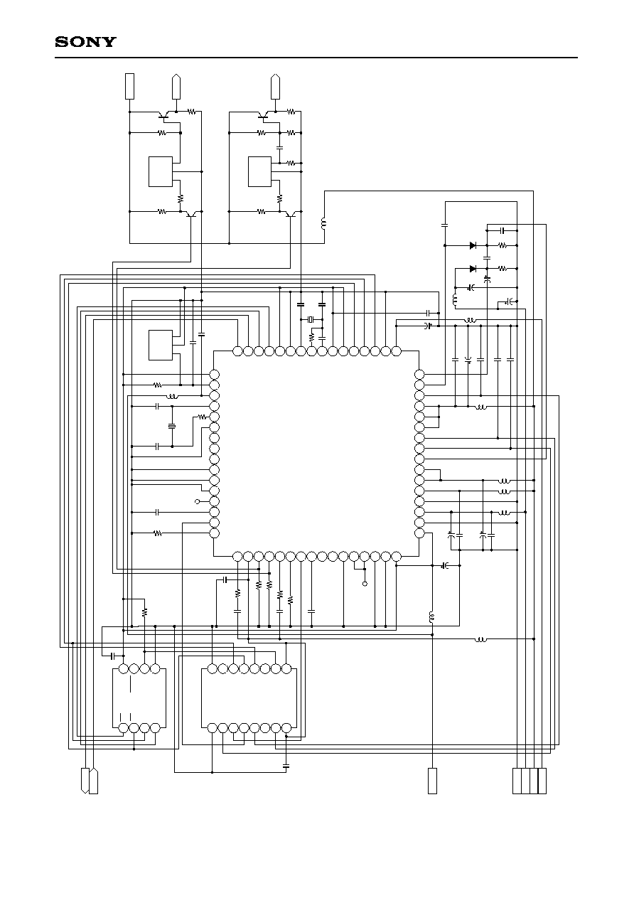
Application Circuit
Application circuits shown are typical examples illustrating the operation of the devices. Sony cannot assume responsibility fo
r
any problems arising out of the use of these circuits or for any infringement of third party patent and other right due to same
.
≠ 18 ≠
MCX18N00A/MCX18N00B
P
A
C
K
A
G
E
S
T
R
U
C
T
U
R
E
P
A
C
K
A
G
E
M
A
T
E
R
I
A
L
L
E
A
D
T
R
E
A
T
M
E
N
T
L
E
A
D
M
A
T
E
R
I
A
L
P
A
C
K
A
G
E
W
E
I
G
H
T
1
6
.
0
8
±
0
.
2
1
s
t
.
p
i
n
I
n
d
e
x
.
5
6
16
.2
64
-
0.8
0
7.6
3.5
±
0
.4
7.3
0 ±
0
.5
8.3
7 ±
0
.5
18
.2
8 ±
0
.3
3
5
∞
2
∞
0
.
3
0
m
i
n
5
.
5
0
m
a
x
3.2
0m
ax
.
5.5
0m
ax
2
-
1
.
5
0
m
a
x
2-1
.5
0m
ax
1
8
.
2
8
±
0
.
3
7
.
6
4
0
4
1
2
5
2
4
ÿ
1.
04
9
8
1
6
4
5
7
3
.
2
0
m
a
x
.
6
4
-
R
(
0
.
2
5
)
P
1
.
0
1
6
X
1
5
=
1
5
.
2
4
6
4
-
0
.
5
0
6
4
p
i
n
Q
F
N
(
7
2
0
m
i
l
)
A
u
4
.
2
0
g
c
e
r
a
m
i
c
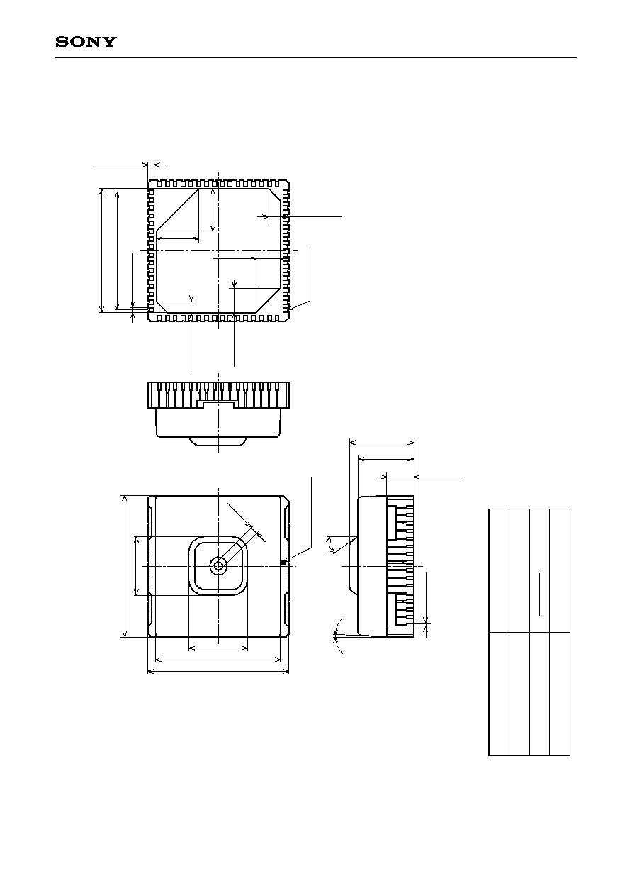
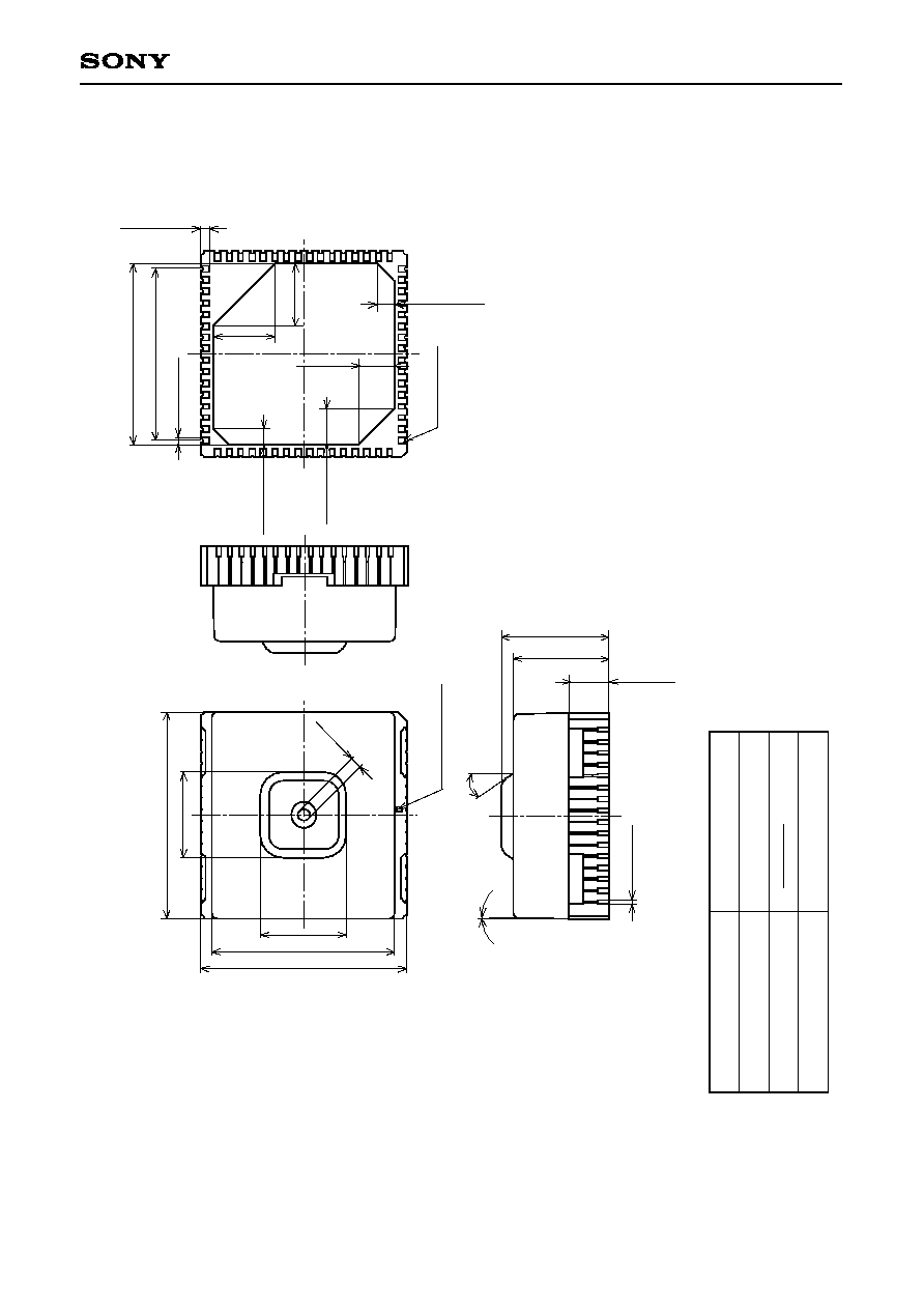
Package Outline
Unit: mm
MCX18N00A
≠ 19 ≠
MCX18N00A/MCX18N00B
P
A
C
K
A
G
E
S
T
R
U
C
T
U
R
E
P
A
C
K
A
G
E
M
A
T
E
R
I
A
L
L
E
A
D
T
R
E
A
T
M
E
N
T
L
E
A
D
M
A
T
E
R
I
A
L
P
A
C
K
A
G
E
W
E
I
G
H
T
1
6
.
0
8
±
0
.
2
1
s
t
.
p
i
n
I
n
d
e
x
.
5
6
16
.2
64
-
0.8
0
7.6
3.5
±
0
.4
8.5
0 ±
0
.5
9.5
7 ±
0
.5
18
.2
8 ±
0
.3
3
5
∞
2
∞
0
.
3
0
m
i
n
5
.
5
0
m
a
x
3.2
0m
ax
.
5.5
0m
ax
2
-
1
.
5
0
m
a
x
2-1
.5
0m
ax
1
8
.
2
8
±
0
.
3
7
.
6
4
0
4
1
2
5
2
4
ÿ
1.
04
9
8
1
6
4
5
7
3
.
2
0
m
a
x
.
6
4
-
R
(
0
.
2
5
)
P
1
.
0
1
6
X
1
5
=
1
5
.
2
4
6
4
-
0
.
5
0
6
4
p
i
n
Q
F
N
(
7
2
0
m
i
l
)
A
u
4
.
2
0
g
c
e
r
a
m
i
c
Package Outline
Unit: mm
MCX18N00B