 | –≠–ª–µ–∫—Ç—Ä–æ–Ω–Ω—ã–π –∫–æ–º–ø–æ–Ω–µ–Ω—Ç: SGM2013N | –°–∫–∞—á–∞—Ç—å:  PDF PDF  ZIP ZIP |
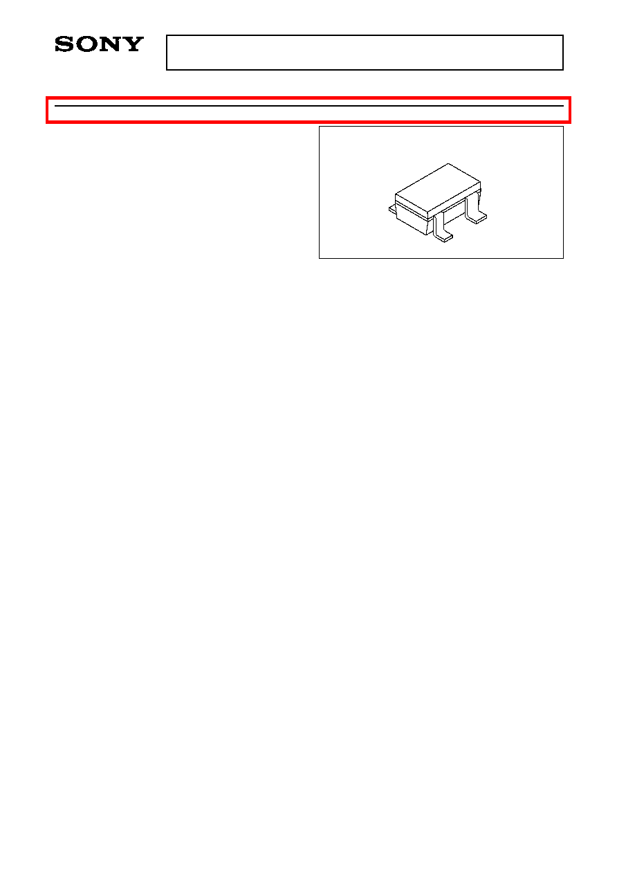
GaAs N-channel Dual-Gate MES FET
Description
The SGM2013N is an N-channel dual-gate GaAs
MES FET for UHF-band low-noise amplification. This
FET is suitable for a wide range of applications
including cellular/cordless phone.
Features
∑ Ultra-small package
∑ Low voltage operation
∑ Low noise NF = 1.4dB (Typ) at 900MHz, NF = 1.7dB (Typ) at 1.5GHz
∑ High gain Ga = 18dB (Typ) at 900MHz, Ga = 16dB (Typ) at 1.5GHz
∑ High stability
∑ Built-in gate protection diode
Application
UHF-band high-frequency amplifier and mixer
Structure
GaAs, N-channel, dual-gate metal semiconductor field-effect transistor
Absolute Maximum Ratings (Ta = 25∞C)
∑ Drain to source voltage
V
DSX
6
V
∑ Gate 1 to source voltage
V
G1S
≠4
V
∑ Gate 2 to source voltage
V
G2S
≠4
V
∑ Drain current
I
D
18
mA
∑ Allowable power dissipation
P
D
100
mW
∑ Channel temperature
Tch
125
∞C
∑ Storage temperature
Tstg
≠55 to +150
∞C
≠ 1 ≠
E97144-PS
Sony reserves the right to change products and specifications without prior notice. This information does not convey any license by
any implication or otherwise under any patents or other right. Application circuits shown, if any, are typical examples illustrating the
operation of the devices. Sony cannot assume responsibility for any problems arising out of the use of these circuits.
SGM2013N
M-281
For the availability of this product, please contact the sales office.
≠ 2 ≠
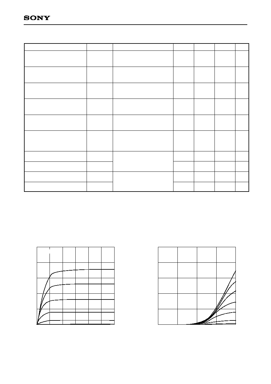
SGM2013N
I
D
vs. V
DS
V
DS
≠ Drain to source voltage [V]
0
1
2
3
4
5
6
0
4
8
12
16
20
(V
G2S
= 0.5V)
I
D
≠
D
r
a
i
n
c
u
r
r
e
n
t
[
m
A
]
I
D
vs. V
G1S
V
G1S
≠ Gate 1 to source voltage [V]
≠2.0
≠1.5
≠1.0
≠0.5
0
0
4
8
12
16
20
(V
DS
= 2V)
I
D
≠
D
r
a
i
n
c
u
r
r
e
n
t
[
m
A
]
≠1.0V
≠0.75V
≠0.5V
≠0.25V
0V
0.25V
V
G2S
= 0.5V
≠1.0V
≠0.8V
≠0.6V
≠0.4V
≠0.2V
V
G1S
= 0V
Typical Characteristics (Ta = 25∞C)
Electrical Characteristics
(Ta = 25∞C)
Item
Gate 1 to source current
Gate 2 to source current
Drain saturation current
Gate 1 to source cut-off
voltage
Gate 2 to source cut-off
voltage
Forward transfer admittance
Input capacitance
Feedback capacitance
Noise figure
NF associated gain
I
G1SS
I
G2SS
I
DSS
V
G1S
(OFF)
V
G2S
(OFF)
gm
Ciss
Crss
NF
Ga
V
G1S
= ≠3V
V
G2S
= 0V
V
DS
= 0V
V
G2S
= ≠3V
V
G1S
= 0V
V
DS
= 0V
V
DS
= 2V
V
G1S
= 0V
V
G2S
= 0V
V
DS
= 2V
I
D
= 100µA
V
G2S
= 0V
V
DS
= 2V
I
D
= 100µA
V
G1S
= 0V
V
DS
= 2V
I
D
= 2mA
V
G2S
= 0.5V
f = 1kHz
V
DS
= 2V
I
D
= 2mA
V
G2S
= 0.5V
f = 1MHz
V
DS
= 2V
I
D
= 2mA
V
G2S
= 0.5V
f = 900MHz
4
8
15
11
0.55
15
1.4
18
≠4
≠4
16
≠1.5
≠1.5
1
30
2.5
µA
µA
mA
V
V
ms
pF
fF
dB
dB
Symbol
Conditions
Min.
Typ.
Max.
Unit
≠ 3 ≠
SGM2013N
I
D
vs. V
G2S
V
G2S
≠ Gate 2 to source voltage [V]
≠2.0
≠1.5
≠1.0
≠0.5
0
0
2
4
6
8
10
(V
DS
= 2V)
I
D
≠
D
r
a
i
n
c
u
r
r
e
n
t
[
m
A
]
≠1.0V
≠0.8V
≠0.6V
≠0.4V
≠0.2V
V
G1S
= 0V
gm vs. V
G1S
V
G1S
≠ Gate 1 source voltage [V]
≠2.0
≠1.5
≠1.0
≠0.5
0
0
5
10
15
20
25
(V
DS
= 2V)
g
m
≠
F
o
r
w
a
r
d
t
r
a
n
s
f
e
r
a
d
m
i
t
t
a
n
c
e
[
m
s
]
≠0.75V
≠0.5V
≠0.25V
0V
0.25V
V
G2S
= 0.5V
NF, Ga vs. V
G1S
V
G1S
≠ Gate 1 to source voltage [V]
≠1.0
≠0.6
≠0.2
0.2
0
1
2
3
4
5
(V
DS
= 2V, V
G2S
= 0.5V, f = 900MHz)
N
F
≠
N
o
i
s
e
f
i
g
u
r
e
[
d
B
]
0
5
10
15
20
25
≠0.8
≠0.4
0
G
a
≠
A
s
s
o
c
i
a
t
e
d
g
a
i
n
[
d
B
]
Ga
NF
NF, Ga vs. V
DS
V
DS
≠ Drain to source voltage [V]
0
2
4
0
1
2
3
4
5
N
F
≠
N
o
i
s
e
f
i
g
u
r
e
[
d
B
]
0
5
10
15
20
25
1
3
5
G
a
≠
A
s
s
o
c
i
a
t
e
d
g
a
i
n
[
d
B
]
Ga
NF
NF, Ga vs. I
D
I
D
≠ Drain current [mA]
0
4
8
11
0
1
2
3
4
5
(V
DS
= 2V, V
G2S
= 0.5V, f = 900MHz)
N
F
≠
N
o
i
s
e
f
i
g
u
r
e
[
d
B
]
0
5
10
15
20
25
2
6
10
G
a
≠
A
s
s
o
c
i
a
t
e
d
g
a
i
n
[
d
B
]
Ga
NF
1
5
9
3
7
NF, Ga vs. f
f ≠ Frequency [GHz]
0
0.8
1.6
2.2
0
1.0
1.5
2.0
2.5
3.0
(V
DS
= 2V, V
G2S
= 0.5V, I
D
= 2mA)
N
F
m
i
n
≠
M
i
n
i
m
u
m
n
o
i
s
e
f
i
g
u
r
e
[
d
B
]
0
5
10
15
25
30
0.4
1.2
2.0
G
a
≠
A
s
s
o
c
i
a
t
e
d
g
a
i
n
[
d
B
]
Ga
0.2
1.0
1.8
0.6
1.4
20
0.5
NFmin
≠ 4 ≠
SGM2013N
S-parameter vs. Frequency Characteristics (V
DS
= 2V, V
G2S
= 0.5V, I
D
= 2mA)
f
(MHz)
200
300
400
500
600
700
800
900
1000
1100
1200
1300
1400
1500
1600
1700
1800
1900
2000
0.98
0.98
0.98
0.98
0.98
0.98
0.98
0.98
0.97
0.97
0.96
0.96
0.96
0.96
0.96
0.96
0.95
0.95
0.95
≠2.0
≠3.1
≠4.0
≠5.2
≠6.1
≠7.2
≠8.3
≠9.7
≠10.5
≠11.7
≠12.7
≠13.8
≠14.8
≠15.9
≠16.9
≠18.0
≠19.0
≠20.0
≠20.6
S22
MAG
ANG
0.00
0.00
0.00
0.00
0.00
0.01
0.01
0.01
0.01
0.01
0.01
0.01
0.01
0.01
0.01
0.01
0.01
0.01
0.01
87.0
85.4
84.7
83.0
81.9
80.3
78.9
77.8
76.9
75.8
75.0
73.8
72.9
72.8
72.5
71.5
70.9
69.7
68.6
S12
MAG
ANG
1.01
1.01
1.01
1.01
1.01
1.01
1.01
1.01
1.01
1.00
1.00
1.00
0.99
0.99
0.99
0.98
0.98
0.97
0.97
172.8
169.3
165.9
162.2
158.7
155.1
151.5
147.8
144.3
140.6
137.2
133.6
130.0
126.5
122.8
119.4
115.7
112.1
108.8
S21
MAG
ANG
0.99
0.99
0.99
0.99
0.98
0.98
0.97
0.96
0.96
0.95
0.94
0.93
0.92
0.91
0.90
0.89
0.88
0.86
0.85
≠4.3
≠6.4
≠8.5
≠10.7
≠12.8
≠15.0
≠17.2
≠19.3
≠21.5
≠23.7
≠26.0
≠28.1
≠30.3
≠32.6
≠34.9
≠37.0
≠39.0
≠41.4
≠43.6
S11
MAG
ANG
Noise Figure Characteristics (V
DS
= 2V, V
G2S
= 0.5V, I
D
= 2mA)
f
(MHz)
200
300
400
500
600
700
800
900
1000
1100
1200
1300
1400
1500
1600
1700
1800
1900
2000
4.2
6.1
8.0
9.8
11.5
13.2
14.8
16.4
18.0
19.6
21.1
22.6
24.2
25.8
27.4
29.1
30.8
32.5
34.4
85.0
83.9
82.9
81.9
80.9
79.9
79.0
78.1
77.2
76.3
75.5
74.7
74.0
73.3
72.6
71.9
71.3
70.7
70.1
MAG
Rn
(
)
0.76
0.80
0.85
0.90
0.96
1.01
1.06
1.11
1.16
1.21
1.26
1.31
1.36
1.41
1.45
1.51
1.56
1.61
1.67
0.99
0.99
0.99
0.98
0.96
0.95
0.93
0.91
0.89
0.87
0.85
0.84
0.82
0.81
0.80
0.80
0.80
0.80
0.80
Gamma Optimum
NFmin
(dB)
ANG
≠ 5 ≠
SGM2013N
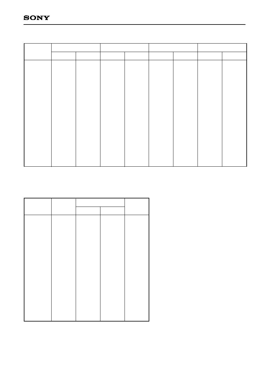
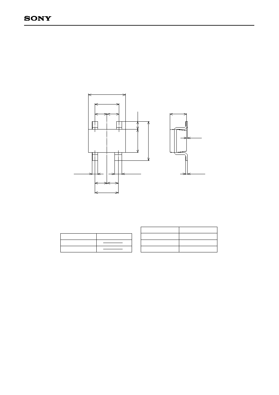
Package Outline
Unit: mm
SONY CODE
EIAJ CODE
JEDEC CODE
PACKAGE MATERIAL
LEAD TREATMENT
LEAD MATERIAL
PACKAGE WEIGHT
EPOXY RESIN
SOLDER PLATING
COPPER
M-281
0.1g
M-281
2.0 ± 0.2
1.3
(0.65)
(0.65)
(0.65)
(0.6)
0.3 ≠ 0.05
+ 0.1
0.4 ≠ 0.05
+ 0.1
0.9 ± 0.1
0 ± 0.1
0.1 ≠ 0.01
+ 0.1
1.25
1
.
2
5
±
0
.
1
2
.
1
±
0
.
2
2
3
4
1
0
.
4
2
5
1 : Source
2 : Gate 1
3 : Gate 2
4 : Drain