 | –≠–ª–µ–∫—Ç—Ä–æ–Ω–Ω—ã–π –∫–æ–º–ø–æ–Ω–µ–Ω—Ç: SLD322V-3 | –°–∫–∞—á–∞—Ç—å:  PDF PDF  ZIP ZIP |
High Power Density 0.5W Laser Diode
Description
The SLD322V is a high power, gain-guided laser diode produced by MOCVD method
1
. Compared to the
SLD300 Series, this laser diode has a high brightness output with a doubled optical density which can be
achieved by QW-SCH structure
2
.
1
MOCVD: Metal Organic Chemical Vapor Deposition
2
QW-SCH: Quantum Well Separate Confinement Heterostructure
Features
∑ High power
Recommended optical power output: Po = 0.5W
∑ Low operating current: Iop = 0.75A (Po = 0.5W)
Applications
∑ Solid state laser excitation
∑ Medical use
∑ Material processes
∑ Measurement
Structure
GaAlAs quantum well structure laser diode
Absolute Maximum Ratings (Tc = 25∞C)
∑ Optical power output
Po
0.55
W
∑ Reverse voltage
V
R
LD
2
V
PD
15
V
∑ Operating temperature (Tc) Topr
≠10 to +30
∞C
∑ Storage temperature
Tstg
≠40 to +85
∞C
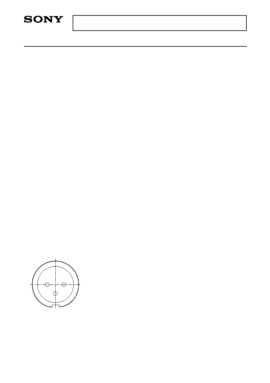
Pin Configuration
≠ 1 ≠
E93205A81-PS
Sony reserves the right to change products and specifications without prior notice. This information does not convey any license by
any implication or otherwise under any patents or other right. Application circuits shown, if any, are typical examples illustrating the
operation of the devices. Sony cannot assume responsibility for any problems arising out of the use of these circuits.
SLD322V
2
Bottom View
1. LD cathode
2. PD anode
3. COMMON
1
3
≠ 2 ≠
SLD322V
Electrical and Optical Characteristics
(Tc: Case temperature, Tc = 25∞C)
Handling Precautions
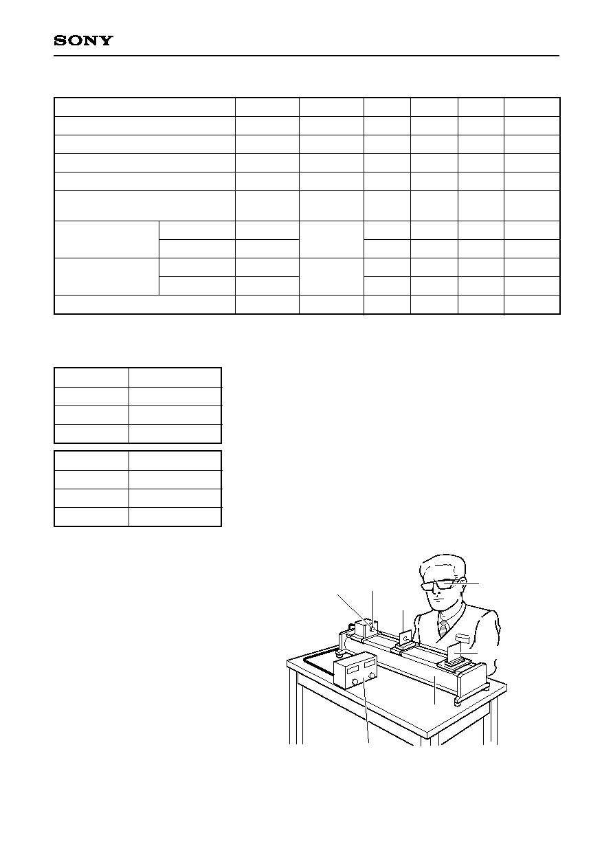
Eye protection against laser beams
The optical output of laser diodes ranges from
several mW to 3W. However the optical power
density of the laser beam at the diode chip
reaches 1MW/cm
2
. Unlike gas lasers, since
laser diode beams are divergent, uncollimated
laser diode beams are fairly safe at a laser
diode. For observing laser beams, ALWAYS use
safety goggles that block infrared rays. Usage of
IR scopes, IR cameras and fluorescent plates is
also recommended for monitoring laser beams
safely.
1
Wavelength Selection Classification
Type
SLD322V-1
SLD322V-2
SLD322V-3
Wavelength (nm)
795 ± 5
810 ± 10
830 ± 10
Type
SLD322V-21
SLD322V-24
SLD322V-25
Wavelength (nm)
798 ± 3
807 ± 3
810 ± 3
AP
C
ATC
Safety goggles for
protection from
laser beam
IR fluorescent plate
Optical
material
Optical power output control device
temperature control device
Lens
Laser diode
Optical boad
Item
Symbol
Conditions
Min.
Typ.
Max.
Unit
Ith
Iop
Vop
p
Imon
//
X,
Y
D
Threshold current
Operating current
Operating voltage
Wavelength
1
Monitor current
Radiation angle
(F. W. H. M.
)
Positional accuracy
Differential efficiency
P
O
= 0.5W
P
O
= 0.5W
P
O
= 0.5W
P
O
= 0.5W
V
R
= 10V
P
O
= 0.5W
P
O
= 0.5W
P
O
= 0.5W
790
0.15
20
4
0.5
0.18
0.75
2.1
0.8
30
9
0.9
0.3
1.2
3.0
840
3.0
40
17
±50
±3
A
A
V
nm
mA
degree
degree
µm
degree
W/A
Perpendicular
Parallel
Position
Angle
F. W. H. M. : Full Width at Half Maximum
≠ 3 ≠
SLD322V
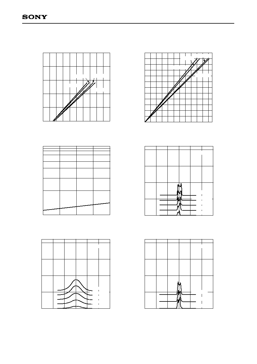
Example of Representative Characteristics
Optical power output vs. Forward current characteristics
I
F
≠ Forward current [mA]
0
200
400
600
800
1000
200
400
600
800
1000
P
o
≠
O
p
t
i
c
a
l
p
o
w
e
r
o
u
t
p
u
t
[
m
W
]
T
C
= ≠10
∞
C
T
C
= 0
∞
C
T
C
= 25
∞
C
T
C
= 30
∞
C
Optical power output vs. Monitor current characteristics
Imon ≠ Monitor current [mA]
0
0.5
1.0
0
250
500
P
o
≠
O
p
t
i
c
a
l
p
o
w
e
r
o
u
t
p
u
t
[
m
W
]
T
C
= ≠10
∞
C
T
C
= 0
∞
C
T
C
= 25
∞
C
T
C
= 30
∞
C
Threshold current vs. Temperature characteristics
Tc ≠ Case temperature [
∞
C]
≠10
0
10
20
30
100
500
1000
I
t
h
≠
T
h
r
e
s
h
o
l
d
c
u
r
r
e
n
t
[
m
A
]
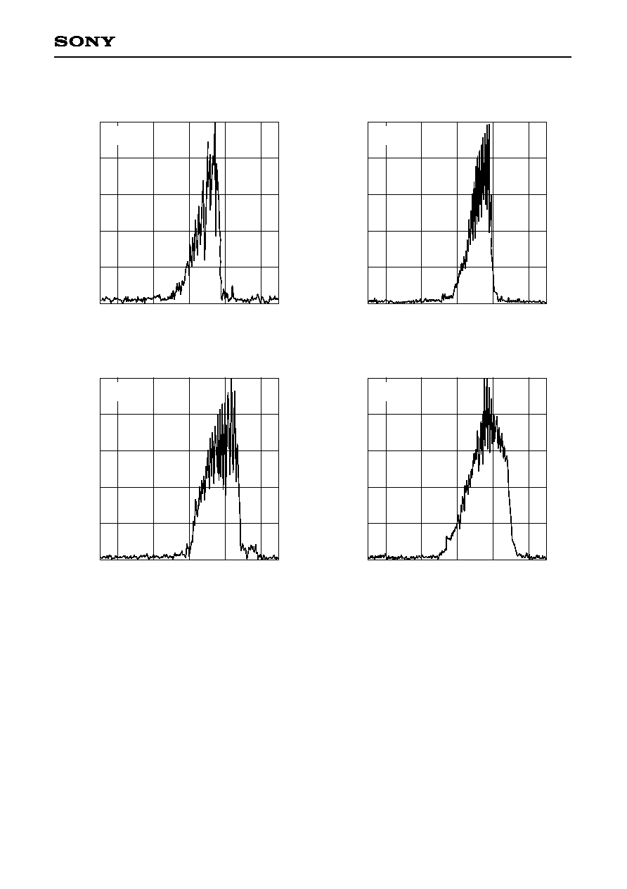
Temperature dependence of far field pattern
(Parallel to junction)
Angle [degree]
≠90
≠60
≠30
0
30
60
90
R
a
d
i
a
t
i
o
n
i
n
t
e
n
s
i
t
y
(
o
p
t
i
o
n
a
l
s
c
a
l
e
)
P
O
= 500mW
T
C
= ≠5
∞
C
T
C
= 10
∞
C
T
C
= 25
∞
C
Power dependence of far field pattern (Parallel to junction)
Angle [degree]
≠90
≠60
≠30
0
30
60
90
R
a
d
i
a
t
i
o
n
i
n
t
e
n
s
i
t
y
(
o
p
t
i
o
n
a
l
s
c
a
l
e
)
T
C
= 25
∞
C
P
O
= 500mW
P
O
= 400mW
P
O
= 300mW
P
O
= 200mW
P
O
= 100mW
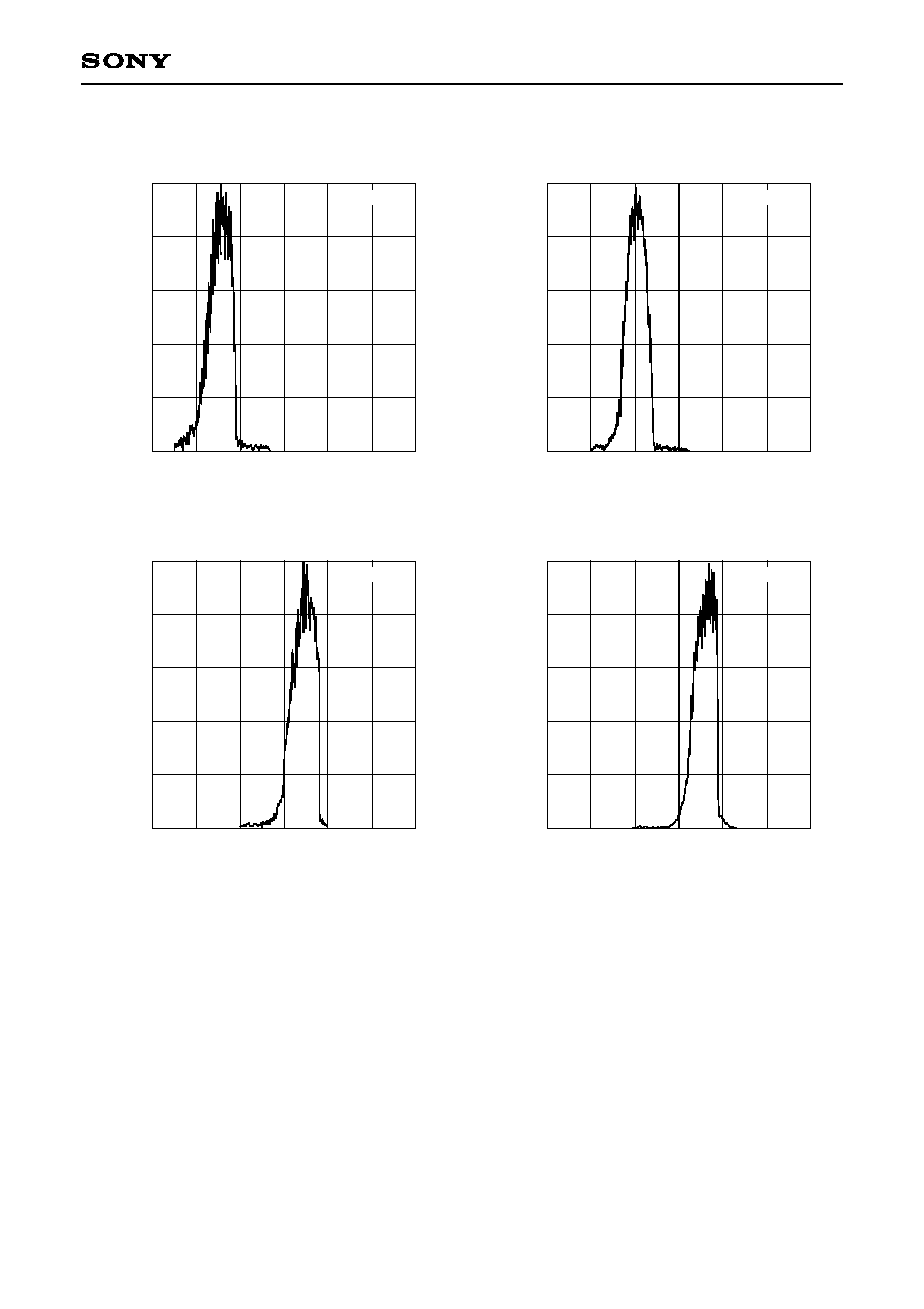
Power dependence of far field pattern
(Perpendicular to junction)
Angle [degree]
≠90
≠60
≠30
0
30
60
90
R
a
d
i
a
t
i
o
n
i
n
t
e
n
s
i
t
y
(
o
p
t
i
o
n
a
l
s
c
a
l
e
)
T
C
= 25
∞
C
P
O
= 500mW
P
O
= 400mW
P
O
= 300mW
P
O
= 200mW
P
O
= 100mW
≠ 4 ≠
SLD322V
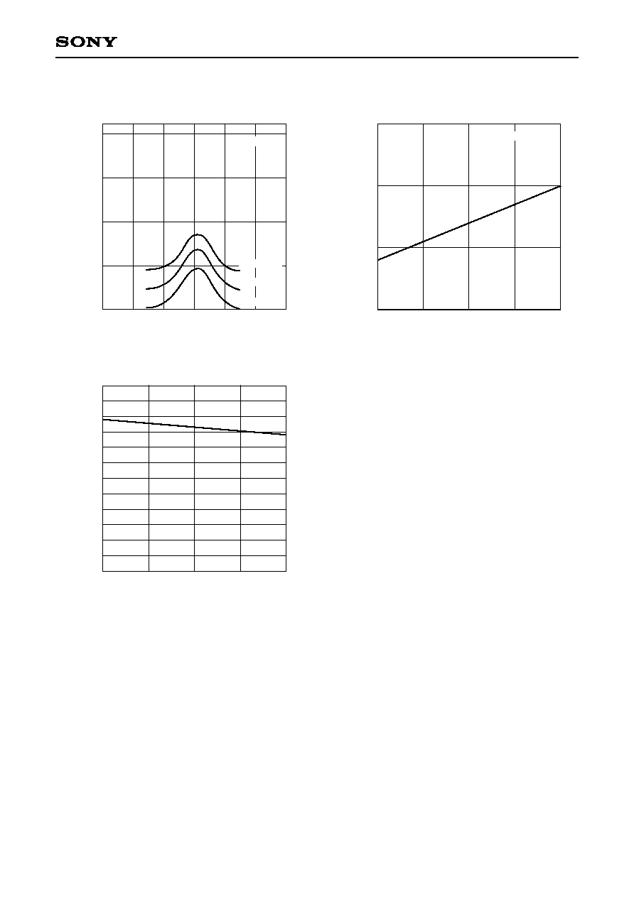
Temperature dependence of far field pattern
(Perpendicular to junction)
Angle [degree]
≠90
≠60
≠30
0
30
60
90
R
a
d
i
a
t
i
o
n
i
n
t
e
n
s
i
t
y
(
o
p
t
i
o
n
a
l
s
c
a
l
e
)
P
O
= 500mW
T
C
= 25
∞
C
T
C
= 10
∞
C
T
C
= ≠5
∞
C
790
800
820
810
p
≠
W
a
v
e
l
e
n
g
t
h
[
n
m
]
Dependence of wavelength
Tc ≠ Case temperature [
∞
C]
≠10
0
10
20
30
Po = 500mW
0
0.5
1.0
D
≠
D
i
f
f
e
r
e
n
t
i
a
l
e
f
f
i
c
i
e
n
c
y
[
m
W
/
m
A
]
Differential efficiency vs. Temperature characteristics
Tc ≠ Case temperature [
∞
C]
≠10
0
10
20
30
≠ 5 ≠
SLD322V
Wavelength [nm]
796
0.2
0.4
0.6
0.8
1.0
804
802
800
798
R
e
l
a
t
i
v
e
r
a
d
i
a
n
t
i
n
t
e
n
s
i
t
y
Tc = 25
∞
C
Po = 0.2W
Wavelength [nm]
796
0.2
0.4
0.6
0.8
1.0
804
802
800
798
R
e
l
a
t
i
v
e
r
a
d
i
a
n
t
i
n
t
e
n
s
i
t
y
Tc = 25
∞
C
Po = 0.4W
Wavelength [nm]
796
0.2
0.4
0.6
0.8
1.0
804
802
800
798
R
e
l
a
t
i
v
e
r
a
d
i
a
n
t
i
n
t
e
n
s
i
t
y
Tc = 25
∞
C
Po = 0.3W
Wavelength [nm]
796
0.2
0.4
0.6
0.8
1.0
804
802
800
798
R
e
l
a
t
i
v
e
r
a
d
i
a
n
t
i
n
t
e
n
s
i
t
y
Tc = 25
∞
C
Po = 0.5W
Power dependence of spectrum
≠ 6 ≠
SLD322V
Wavelength [nm]
790
0.2
0.4
0.6
0.8
1.0
815
810
805
800
785
795
R
e
l
a
t
i
v
e
r
a
d
i
a
n
t
i
n
t
e
n
s
i
t
y
Tc = ≠10
∞
C
Wavelength [nm]
790
0.2
0.4
0.6
0.8
1.0
815
810
805
800
785
795
R
e
l
a
t
i
v
e
r
a
d
i
a
n
t
i
n
t
e
n
s
i
t
y
Tc = 25
∞
C
Wavelength [nm]
790
0.2
0.4
0.6
0.8
1.0
815
810
805
800
785
795
R
e
l
a
t
i
v
e
r
a
d
i
a
n
t
i
n
t
e
n
s
i
t
y
Tc = 30
∞
C
Wavelength [nm]
790
0.2
0.4
0.6
0.8
1.0
815
810
805
800
785
795
R
e
l
a
t
i
v
e
r
a
d
i
a
n
t
i
n
t
e
n
s
i
t
y
Tc = 0
∞
C
Temperature dependence of spectrum (Po = 0.5W)
≠ 7 ≠
SLD322V
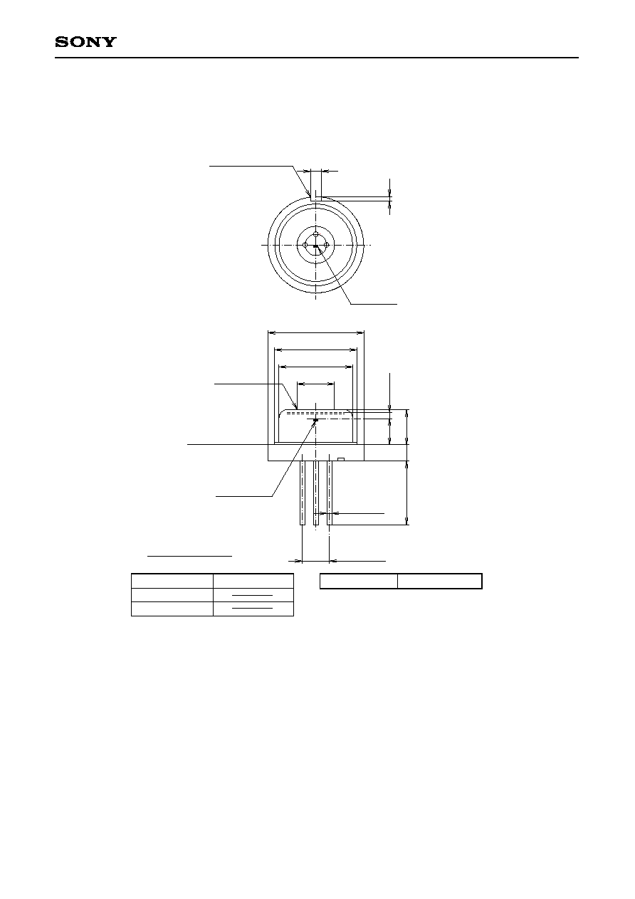
Package Outline
Unit: mm
M-248 (LO-11)
Reference
Slot
1.0
0
.
4
Photo
Diode
2
3
1
Window
Glass
Reference
Plane
LD Chip
9.0 ≠ 0.015
0
7.7 MAX
6.9 MAX
3.5
0
.
6
M
A
X
2
.
4
5
3
.
4
M
A
X
1
.
5
7
.
0
M
A
X
3 ≠
0.45
PCD
2.54
Optical
Distance = 2.55 ± 0.05
SONY CODE
EIAJ CODE
JEDEC CODE
M-248
PACKAGE WEIGHT
1.2g