0.5W High Power Laser Diode
Description
The SLD322XT is a high power, gain-guided laser diode produced
by MOCVD method
1
. Compared to the SLD300 Series, this laser
diode has a high brightness output with a doubled optical density
which can be achived by QW-SCH structure
2
.
Fine adjustment of the oscillation wavelength is possible by controlling
the temperature using the built-in TE cooler (Peltier element).
1
MOCVD: Metal Organic Chemical Vapor Deposition
2
QW-SCH: Quantum Well Separate Confinement Heterostructure
Features
∑ High power
Recommended optical power output: Po = 0.5W
∑ Low operating current: Iop = 0.75A (Po = 0.5W)
∑ Flat package with built-in photodiode, TE cooler, and thermistor
Applications
∑ Solid state laser excitation
∑ Medical use
∑ Material processes
∑ Measurement
Structure
AlGaAs quantum well structure laser diode
Operating Lifetime
MTTF 10,000H (effective value) at Po = 0.5W, Tth = 25∞C
Absolute Maximum Ratings (Tth = 25∞C)
∑ Optical power output
Po
0.55
W
∑ Reverse voltage
V
R
LD
2
V
PD
15
V
∑ Operating temperature (Tth)
Topr
≠10 to +30
∞C
∑ Storage temperature
Tstg
≠40 to +85
∞C
≠ 1 ≠
E93206B02-PS
Sony reserves the right to change products and specifications without prior notice. This information does not convey any license by
any implication or otherwise under any patents or other right. Application circuits shown, if any, are typical examples illustrating the
operation of the devices. Sony cannot assume responsibility for any problems arising out of the use of these circuits.
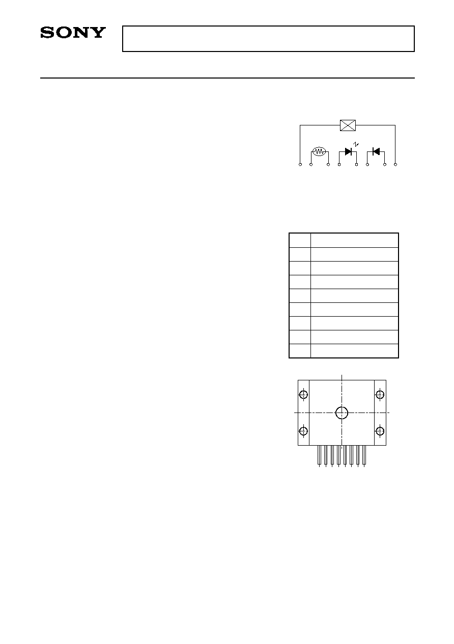
SLD322XT
1
2
T
H
LD
TE Cooler
PD
P
N
3
4
5
6
7
8
1
8
Equivalent Circuit
No.
1
2
3
4
5
6
7
8
Function
TE cooler (negative)
Thermistor lead 1
Thermistor lead 2
Laser diode (anode)
Laser diode (cathode)
Photodiode (cathode)
Photodiode (anode)
TE cooler (positive)
Pin Configuration (Top View)
Warranty
This warranty period shall be 90 days after receipt of the product or
1,000 hours operation time whichever is shorter.
Sony Quality Assurance Department shall analyze any product that
fails during said warranty period, and if the analysis results show
that the product failed due to material or manufacturing defects on
the part of Sony, the product shall be replaced free of charge.
Laser diodes naturally have differing lifetimes which follow a Weibull
distribution.
Special warranties are also available.

≠ 2 ≠
SLD322XT
Electrical and Optical Characteristics
(Tth: Thermistor temperature, Tth = 25∞C)
Handling Precautions
Eye protection against laser beams
The optical output of laser diodes ranges from
several mW to 3W. However the optical power
density of the laser beam at the diode chip
reaches 1MW/cm
2
. Unlike gas lasers, since
laser diode beams are divergent, uncollimated
laser diode beams are fairly safe at a laser
diode. For observing laser beams, ALWAYS use
safety goggles that block infrared rays. Usage of
IR scopes, IR cameras and fluorescent plates is
also recommended for monitoring laser beams
safely.
Item
Symbol
Conditions
Min.
Typ.
Max.
Unit
Ith
Iop
Vop
p
Imon
//
X,
Y
D
Rth
Threshold current
Operating current
Operating voltage
Wavelength
Monitor current
Radiation angle
Positional accuracy
Differential efficiency
Thermistor resistance
P
O
= 0.5W
P
O
= 0.5W
P
O
= 0.5W
P
O
= 0.5W
V
R
= 10V
P
O
= 0.5W
P
O
= 0.5W
P
O
= 0.5W
Tth = 25∞C
790
0.15
20
4
0.5
0.18
0.75
2.1
0.8
30
9
0.9
10
0.3
1.2
3.0
840
3.0
40
17
±100
±3
A
A
V
nm
mA
degree
degree
µm
degree
W/A
k
Perpendicular
Parallel
Position
Angle
Wavelength Selection Classification
Type
SLD322XT-1
SLD322XT-2
SLD322XT-3
Wavelength (nm)
795 ± 5
810 ± 10
830 ± 10
Type
SLD322XT-21
SLD322XT-24
SLD322XT-25
Wavelength (nm)
798 ± 3
807 ± 3
810 ± 3
AP
C
ATC
Safety goggles for
protection from
laser beam
IR fluorescent plate
Optical
material
Optical power output control device
temperature control device
Lens
Laser diode
Optical boad
≠ 3 ≠
SLD322XT
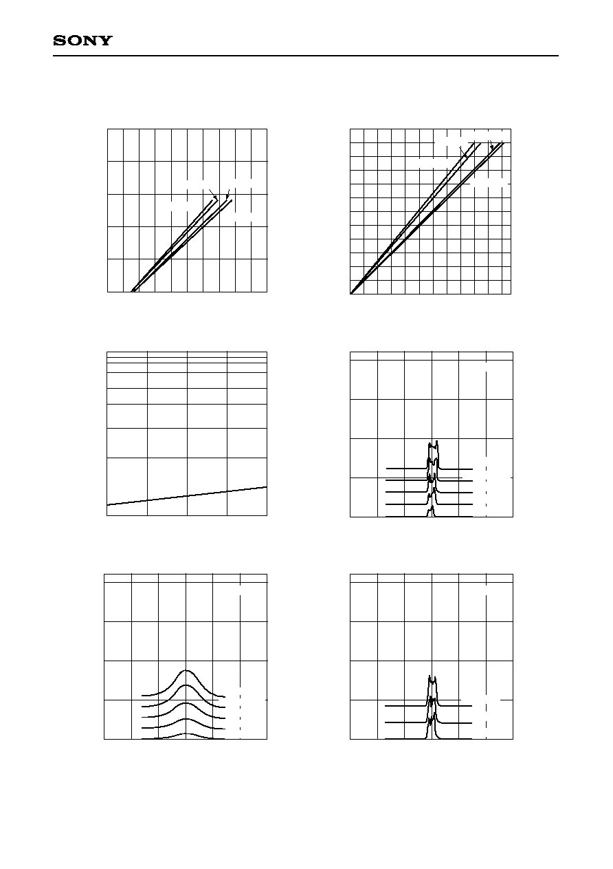
Example of Representative Characteristics
Optical power output vs. Forward current characteristics
I
F
≠ Forward current [mA]
0
200
400
600
800
1000
200
400
600
800
1000
P
o
≠
O
p
t
i
c
a
l
p
o
w
e
r
o
u
t
p
u
t
[
m
W
]
Tth = ≠10
∞
C
Tth = 0
∞
C
Tth = 25
∞
C
Tth = 30
∞
C
Optical power output vs. Monitor current characteristics
Imon ≠ Monitor current [mA]
0
0.5
1.0
0
250
500
P
o
≠
O
p
t
i
c
a
l
p
o
w
e
r
o
u
t
p
u
t
[
m
W
]
Tth = ≠10
∞
C
Tth = 0
∞
C
Tth = 25
∞
C
Tth = 30
∞
C
Threshold current vs. Temperature characteristics
Tth ≠ Thermistor temperature [
∞
C]
≠10
0
10
20
30
100
500
1000
I
t
h
≠
T
h
r
e
s
h
o
l
d
c
u
r
r
e
n
t
[
m
A
]
Temperature dependence of far field pattern
(Parallel to junction)
Angle [degree]
≠90
≠60
≠30
0
30
60
90
R
a
d
i
a
t
i
o
n
i
n
t
e
n
s
i
t
y
(
o
p
t
i
o
n
a
l
s
c
a
l
e
)
P
O
= 500mW
Tth = ≠5
∞
C
Tth = 10
∞
C
Tth = 25
∞
C
Power dependence of far field pattern
(Parallel to junction)
Angle [degree]
≠90
≠60
≠30
0
30
60
90
R
a
d
i
a
t
i
o
n
i
n
t
e
n
s
i
t
y
(
o
p
t
i
o
n
a
l
s
c
a
l
e
)
Tth = 25
∞
C
P
O
= 500mW
P
O
= 400mW
P
O
= 300mW
P
O
= 200mW
P
O
= 100mW
Power dependence of far field pattern
(Perpendicular to junction)
Angle [degree]
≠90
≠60
≠30
0
30
60
90
R
a
d
i
a
t
i
o
n
i
n
t
e
n
s
i
t
y
(
o
p
t
i
o
n
a
l
s
c
a
l
e
)
Tth = 25
∞
C
P
O
= 500mW
P
O
= 400mW
P
O
= 300mW
P
O
= 200mW
P
O
= 100mW
≠ 4 ≠
SLD322XT
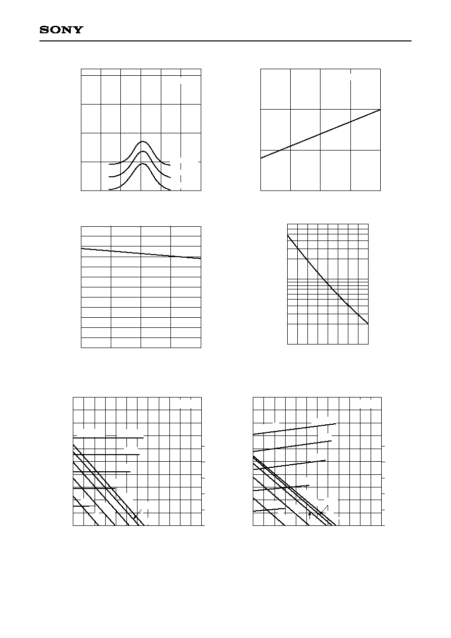
Temperature dependence of far field pattern
(Perpendicular to junction)
Angle [degree]
≠90
≠60
≠30
0
30
60
90
R
a
d
i
a
t
i
o
n
i
n
t
e
n
s
i
t
y
(
o
p
t
i
o
n
a
l
s
c
a
l
e
)
P
O
= 500mW
Tth = 25
∞
C
Tth = 10
∞
C
Tth = ≠5
∞
C
790
800
820
810
l
p
≠
W
a
v
e
l
e
n
g
t
h
[
n
m
]
Dependence of wavelength
Tth ≠ Thermistor temperature [
∞
C]
≠10
0
10
20
30
Po = 500mW
0
0.5
1.0
D
≠
D
i
f
f
e
r
e
n
t
i
a
l
e
f
f
i
c
i
e
n
c
y
[
W
/
A
]
Differential efficiency vs. Temperature characteristics
Tth ≠ Thermistor temperature [
∞
C]
≠10
0
10
20
30
10
5
0
50
0
T [
∞
C]
TE cooler characteristics 2
Q
≠
A
b
s
o
r
b
e
d
h
e
a
t
[
W
]
100
Tth = 25
∞
C
2.0A
1.5A
2.5
A
2.0A
1.5A
1
.0
A
0
.5
A
T
VS
V
T
VS
Q
0.5A
5
4
3
2
1
0
V
T
≠
P
i
n
v
o
l
t
a
g
e
[
V
]
1.0A
I
T
= 2.5A
0
10
5
0
50
T ≠ Temperature difference [
∞
C]
T: Tc ≠ Tth
Tth: Thermistor temperature
Tc: Case temperature
TE cooler characteristics 1
Q
≠
A
b
s
o
r
b
e
d
h
e
a
t
[
W
]
100
Tc = 33
∞
C
2.0A
1.5A
2
.5
A
2.0A
0
.5
A
1
.0
A
1
.5
A
T
VS
V
T
T
V
S
Q
0.5A
5
4
3
2
1
0
V
T
≠
P
i
n
v
o
l
t
a
g
e
[
V
]
1.0A
I
T
= 2.5A
R
t
h
≠
T
h
e
r
m
i
s
t
o
r
r
e
s
i
s
t
a
n
c
e
[
k
]
50
10
5
1
≠10 0
10 20 30 40 50 60 70
Thermistor characteristics
Tth ≠ Thermistor temperature [
∞
C]
TE cooler characteristics
≠ 5 ≠
SLD322XT
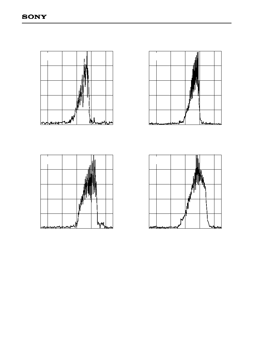
Wavelength [nm]
796
0.2
0.4
0.6
0.8
1.0
804
802
800
798
R
e
l
a
t
i
v
e
r
a
d
i
a
n
t
i
n
t
e
n
s
i
t
y
Tth = 25
∞
C
Po = 0.2W
Wavelength [nm]
796
0.2
0.4
0.6
0.8
1.0
804
802
800
798
R
e
l
a
t
i
v
e
r
a
d
i
a
n
t
i
n
t
e
n
s
i
t
y
Tth = 25
∞
C
Po = 0.4W
Wavelength [nm]
796
0.2
0.4
0.6
0.8
1.0
804
802
800
798
R
e
l
a
t
i
v
e
r
a
d
i
a
n
t
i
n
t
e
n
s
i
t
y
Tth = 25
∞
C
Po = 0.3W
Wavelength [nm]
796
0.2
0.4
0.6
0.8
1.0
804
802
800
798
R
e
l
a
t
i
v
e
r
a
d
i
a
n
t
i
n
t
e
n
s
i
t
y
Tth = 25
∞
C
Po = 0.5W
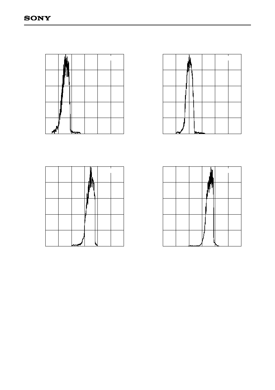
Power dependence of spectrum
≠ 6 ≠
SLD322XT
Wavelength [nm]
790
0.2
0.4
0.6
0.8
1.0
815
810
805
800
785
795
R
e
l
a
t
i
v
e
r
a
d
i
a
n
t
i
n
t
e
n
s
i
t
y
Tth = ≠10
∞
C
Wavelength [nm]
790
0.2
0.4
0.6
0.8
1.0
815
810
805
800
785
795
R
e
l
a
t
i
v
e
r
a
d
i
a
n
t
i
n
t
e
n
s
i
t
y
Tth = 25
∞
C
Wavelength [nm]
790
0.2
0.4
0.6
0.8
1.0
815
810
805
800
785
795
R
e
l
a
t
i
v
e
r
a
d
i
a
n
t
i
n
t
e
n
s
i
t
y
Tth = 30
∞
C
Wavelength [nm]
790
0.2
0.4
0.6
0.8
1.0
815
810
805
800
785
795
R
e
l
a
t
i
v
e
r
a
d
i
a
n
t
i
n
t
e
n
s
i
t
y
Tth = 0
∞
C
Temperature dependence of spectrum (Po = 0.5W)

≠ 7 ≠
SLD322XT
Package Outline
Unit: mm
M ≠ 273(LO ≠ 10)
SONY CODE
EIAJ CODE
JEDEC CODE
PACKAGE STRUCTURE
M-273(LO-10)
33.0 ± 0.05
1
5
.
0
±
0
.
0
5
ÿ5.0
4 ≠ R1.2 ± 0.3
Window
Glass
8 ≠ ÿ0.6
2.54
*
7
.
5
±
0
.
1
1
4
.
0
2
8
.
0
±
0
.
5
38.0 ± 0.5
19.0
LD Chip
28.0 ± 0.5
16.5 ± 0.1
3
.
0
7
.
5
±
0
.
2
1
1
.
3
5
±
0
.
1
0
.
6
5
M
A
X
1
0
.
4
Reference Plane
*
*Distance between pilot hole and emittng area
4 ≠ ÿ3.0
0
+ 0.05
+
2
.
0
8
.
0
≠
1
.
0
PACKAGE WEIGHT
43g
Sony Corporation