
July 2003
The following document specifies Spansion memory products that are now offered by both Advanced
Micro Devices and Fujitsu. Although the document is marked with the name of the company that orig-
inally developed the specification, these products will be offered to customers of both AMD and
Fujitsu.
Continuity of Specifications
There is no change to this datasheet as a result of offering the device as a Spansion product. Any
changes that have been made are the result of normal datasheet improvement and are noted in the
document revision summary, where supported. Future routine revisions will occur when appropriate,
and changes will be noted in a revision summary.
Continuity of Ordering Part Numbers
AMD and Fujitsu continue to support existing part numbers beginning with "Am" and "MBM". To order
these products, please use only the Ordering Part Numbers listed in this document.
For More Information
Please contact your local AMD or Fujitsu sales office for additional information about Spansion
memory solutions.
Am29LV640MT/B
Data Sheet
Publication Number 26190 Revision C Amendment +3 Issue Date February 12, 2004
For new designs, S29GL064M supercedes Am29LV640MT/B and is the factory-recommended migra-
tion path for this device. Please refer to the S29GLxxxM Family Datasheet for specifications and
ordering information.

This document contains information on a product under development at Advanced Micro Devices. The information
is intended to help you evaluate this product. AMD reserves the right to change or discontinue work on this proposed
product without notice.
Publication# 26190
Rev: C Amendment/+3
Issue Date: February 12, 2004
Refer to AMD's Website (www.amd.com) for the latest information.
For new designs, S29GL064M supercedes Am29LV640MT/B and is the factory-recommended migration path
for this device. Please refer to the S29GLxxxM Family Datasheet for specifications and ordering information.
Am29LV640MT/B
64 Megabit (4 M x 16-Bit/8 M x 8-Bit) MirrorBit
TM
3.0 Volt-only Boot Sector Flash Memory
DISTINCTIVE CHARACTERISTICS
ARCHITECTURAL ADVANTAGES
Single power supply operation
-- 3 V for read, erase, and program operations
Manufactured on 0.23 µm MirrorBit process
technology
SecSi
TM
(Secured Silicon) Sector region
-- 128-word/256-byte sector for permanent, secure
identification through an 8-word/16-byte random
Electronic Serial Number, accessible through a
command sequence
-- May be programmed and locked at the factory or by
the customer
Flexible sector architecture
-- One hundred twenty-seven 32 Kword/64-Kbyte
sectors
-- Eight 4 Kword/8 Kbyte boot sectors
Compatibility with JEDEC standards
-- Provides pinout and software compatibility for
single-power supply flash, and superior inadvertent
write protection
Minimum 100,000 erase cycle guarantee per sector
20-year data retention at 125
∞
C
PERFORMANCE CHARACTERISTICS
High performance
-- 90 ns access time
-- 25 ns page read times
-- 0.5 s typical sector erase time
-- 22 µs typical effective write buffer word programming
time: 16-word/32-byte write buffer reduces overall
programming time for multiple-word/byte updates
-- 4-word/8-byte page read buffer
-- 16-word/32-byte write buffer
Low power consumption (typical values at 3.0 V, 5
MHz)
-- 30 mA typical active read current
-- 50 mA typical erase/program current
-- 1 µA typical standby mode current
Package options
-- 48-pin TSOP
-- 63-ball Fine-pitch BGA
-- 64-ball Fortified BGA
SOFTWARE & HARDWARE FEATURES
Software features
-- Program Suspend & Resume: read other sectors
before programming operation is completed
-- Erase Suspend & Resume: read/program other
sectors before an erase operation is completed
-- Data# polling & toggle bits provide status
-- Unlock Bypass Program command reduces overall
multiple-word programming time
-- CFI (Common Flash Interface) compliant: allows host
system to identify and accommodate multiple flash
devices
Hardware features
-- Sector Group Protection: hardware-level method of
preventing write operations within a sector group
-- Temporary Sector Unprotect: V
ID
-level method of
changing code in locked sectors
-- WP#/ACC input:
Write Protect input (WP#) protects top or bottom two
sectors regardless of sector protection settings
ACC (high voltage) accelerates programming time for
higher throughput during system production
-- Hardware reset input (RESET#) resets device
-- Ready/Busy# output (RY/BY#) indicates program or
erase cycle completion

2
Am29LV640MT/B
February 12, 2004
A D V A N C E I N F O R M A T I O N
GENERAL DESCRIPTION
The Am29LV640MT/B is a 64 Mbit, 3.0 volt single
power supply flash memory device organized as
4,194,304 words or 8,388,608 bytes. The device has
an 8-bit/16-bit bus and can be programmed either in
the host system or in standard EPROM programmers.
An access time of 90, 100, 110, or 120 ns is available.
Note that each access time has a specific operating
voltage range (V
CC
) and an I/O voltage range (V
IO
), as
specified in the
Product Selector Guide
and the
Order-
ing Information
sections. The device is offered in a
48-pin TSOP, 63-ball Fine-pitch BGA or 64-ball Forti-
fied BGA package. Each device has separate chip en-
able (CE#), write enable (WE#) and output enable
(OE#) controls.
Each device requires only a single 3.0 volt power
supply for both read and write functions. In addition to
a V
CC
input, a high-voltage accelerated program
(ACC) function provides shorter programming times
through increased current on the WP#/ACC input. This
feature is intended to facilitate factory throughput dur-
ing system production, but may also be used in the
field if desired.
The device is entirely command set compatible with
the JEDEC single-power-supply Flash standard.
Commands are written to the device using standard
microprocessor write timing. Write cycles also inter-
nally latch addresses and data needed for the pro-
gramming and erase operations.
The sector erase architecture allows memory sec-
tors to be erased and reprogrammed without affecting
the data contents of other sectors. The device is fully
erased when shipped from the factory.
Device programming and erasure are initiated through
command sequences. Once a program or erase oper-
ation has begun, the host system need only poll the
DQ7 (Data# Polling) or DQ6 (toggle) status bits or
monitor the Ready/Busy# (RY/BY#) output to deter-
mine whether the operation is complete. To facilitate
programming, an Unlock Bypass mode reduces com-
mand sequence overhead by requiring only two write
cycles to program data instead of four.
Hardware data protection measures include a low
V
CC
detector that automatically inhibits write opera-
tions during power transitions. The hardware sector
protection feature disables both program and erase
operations in any combination of sectors of memory.
This can be achieved in-system or via programming
equipment.
The Erase Suspend/Erase Resume feature allows
the host system to pause an erase operation in a given
sector to read or program any other sector and then
complete the erase operation. The Program Sus-
pend/Program Resume feature enables the host sys-
tem to pause a program operation in a given sector to
read any other sector and then complete the program
operation.
The hardware RESET# pin terminates any operation
in progress and resets the device, after which it is then
ready for a new operation. The RESET# pin may be
tied to the system reset circuitry. A system reset would
thus also reset the device, enabling the host system to
read boot-up firmware from the Flash memory device.
T h e d evice re d uce s p ow er co ns ump ti on i n th e
standby mode when it detects specific voltage levels
on CE# and RESET#, or when addresses have been
stable for a specified period of time.
The Write Protect (WP#) feature protects the top or
bottom two sectors by asserting a logic low on the
WP#/ACC pin. The protected sector will still be pro-
tected even during accelerated programming.
The SecSi
TM
(Secured Silicon) Sector provides a
128-word/256-byte area for code or data that can be
permanently protected. Once this sector is protected,
no further changes within the sector can occur.
AMD MirrorBit flash technology combines years of
Flash memory manufacturing experience to produce
the highest levels of quality, reliability and cost effec-
tiveness. The device electrically erases all bits within a
sector simultaneously via hot-hole assisted erase. The
data is programmed using hot electron injection.
February 12, 2004
Am29LV640MT/B
3
A D V A N C E I N F O R M A T I O N
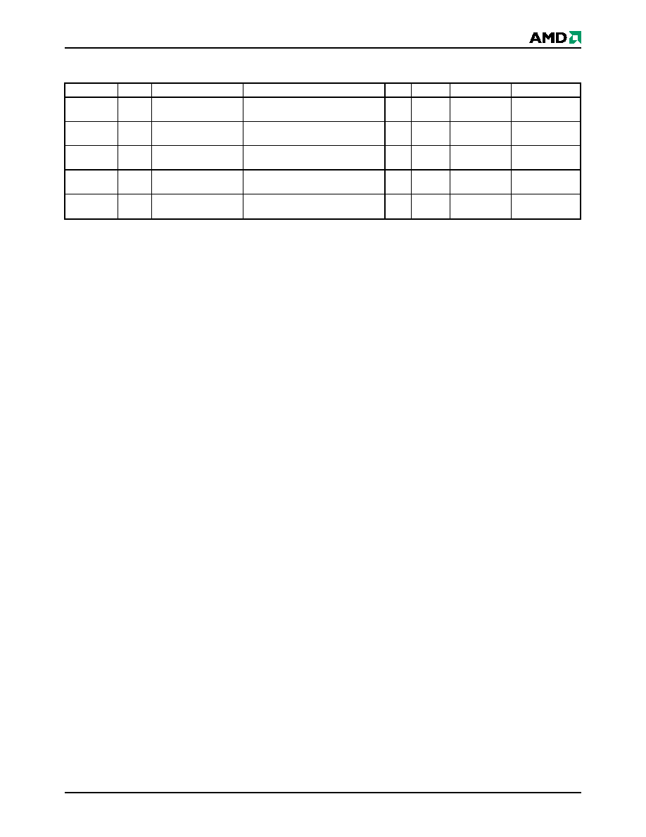
MIRRORBIT 64 MBIT DEVICE FAMILY
RELATED DOCUMENTS
To download related documents, click on the following
links or go to www.amd.com
Flash Memory
Prod-
uct Information
MirrorBit
Flash Information
Tech-
nical Documentation.
MirrorBitTM Flash Memory Write Buffer Programming
and Page Buffer Read
Implementing a Common Layout for AMD MirrorBit
and Intel StrataFlash Memory Devices
Migrating from Single-byte to Three-byte Device IDs
AMD MirrorBitTM White Paper
Device
Bus
Sector Architecture
Packages
V
IO
RY/BY#
WP#, ACC
WP# Protection
LV065MU
x8
Uniform (64 Kbyte)
48-pin TSOP (std. & rev. pinout),
63-ball FBGA
Yes
Yes
ACC only
No WP#
LV640MT/B
x8/x16
Boot (8 x 8 Kbyte
at top & bottom)
48-pin TSOP, 63-ball Fine-pitch BGA,
64-ball Fortified BGA
No
Yes
WP#/ACC pin
2 x 8 Kbyte
top or bottom
LV640MH/L
x8/x16
Uniform (64 Kbyte)
56-pin TSOP (std. & rev. pinout),
64-ball Fortified BGA
Yes
Yes
WP#/ACC pin
1 x 64 Kbyte
high or low
LV641MH/L
x16
Uniform (32 Kword)
48-pin TSOP (std. & rev. pinout)
Yes
No
Separate WP#
and ACC pins
1 x 32 Kword
top or bottom
LV640MU
x16
Uniform (32 Kword)
64-ball Fortified BGA,
63-ball Fine-pitch BGA
Yes
Yes
ACC only
No WP#
