
July 2003
The following document specifies Spansion memory products that are now offered by both Advanced
Micro Devices and Fujitsu. Although the document is marked with the name of the company that orig-
inally developed the specification, these products will be offered to customers of both AMD and
Fujitsu.
Continuity of Specifications
There is no change to this datasheet as a result of offering the device as a Spansion product. Any
changes that have been made are the result of normal datasheet improvement and are noted in the
document revision summary, where supported. Future routine revisions will occur when appropriate,
and changes will be noted in a revision summary.
Continuity of Ordering Part Numbers
AMD and Fujitsu continue to support existing part numbers beginning with "Am" and "MBM". To order
these products, please use only the Ordering Part Numbers listed in this document.
For More Information
Please contact your local AMD or Fujitsu sales office for additional information about Spansion
memory solutions.
Am29LV652D
Data Sheet
Publication Number 24961 Revision A Amendment +4 Issue Date October 29, 2004

THIS PAGE LEFT INTENTIONALLY BLANK.

PRELIMINARY
This Data Sheet states AMD's current technical specifications regarding the Products described herein. This Data
Sheet may be revised by subsequent versions or modifications due to changes in technical specifications.
Publication# 24961
Rev: A Amendment/+4
Issue Date: October 29, 2004
Refer to AMD's Website (www.amd.com) for the latest information.
Am29LV652D
128 Megabit (16 M x 8-Bit) CMOS 3.0 Volt-only
Uniform Sector Flash Memory with VersatileIO
TM Control
DISTINCTIVE CHARACTERISTICS
Two 64 Megabit (Am29LV065D) in a single 63-ball 11
x 12 mm FBGA package (Note: Features will be
described for each internal Am29LV065D)
Two Chip Enable inputs
-- Each CE# controls selection of one internal
Am29LV065D device
Single power supply operation
-- 3.0 to 3.6 volt read, erase, and program operations
VersatileIO
TM control
-- Device generates output voltages and tolerates input
voltages on DQ I/Os as determined by the voltage on
V
IO
input
High performance
-- Access times as fast as 90 ns
Manufactured on 0.23 µm process technology
CFI (Common Flash Interface) compliant
-- Provides device-specific information to the system,
allowing host software to easily reconfigure for
different Flash devices
Ultra low power consumption (typical values at 3.0 V,
5 MHz) for the part
-- 9 mA typical active read current
-- 26 mA typical erase/program current
-- 400 nA typical standby mode current
Flexible sector architecture
-- Two hundred fifty-six 64 Kbyte sectors
Sector Protection
-- A hardware method to lock a sector to prevent
program or erase operations within that sector
-- Sectors can be locked in-system or via programming
equipment
-- Temporary Sector Unprotect feature allows code
changes in previously locked sectors
Embedded Algorithms
-- Embedded Erase algorithm automatically
preprograms and erases the entire chip or any
combination of designated sectors
-- Embedded Program algorithm automatically writes
and verifies data at specified addresses
Compatibility with JEDEC standards
-- Except for the added CE2#, the FBGA is pinout and
software compatible with single-power supply Flash
-- Superior inadvertent write protection
Minimum 1 million erase cycle guarantee per sector
63-ball FBGA Package
Erase Suspend/Erase Resume
-- Suspends an erase operation to read data from, or
program data to, a sector that is not being erased,
then resumes the erase operation
Data# Polling and toggle bits
-- Provides a software method of detecting program or
erase operation completion
Unlock Bypass Program command
-- Reduces overall programming time when issuing
multiple program command sequences
Ready/Busy# output (RY/BY#)
-- Provides a hardware method of detecting program or
erase cycle completion
Hardware reset input (RESET#)
-- Hardware method to reset the device for reading array
data
ACC input
-- Accelerates programming time for higher throughput
during system production
Program and Erase Performance (V
HH
not applied to
the ACC input)
-- Byte program time: 5 µs typical
-- Sector erase time: 1.6 s typical for each 64 Kbyte
sector
20-year data retention at 125
∞C
-- Reliable operation for the life of the system

2
Am29LV652D
October 29, 2004
P R E L I M I N A R Y
GENERAL DESCRIPTION
The Am29LV652D is a 128 Mbit, 3.0 Volt (3.0 V to 3.6
V) single power supply flash memory device organized
as two Am29LV065D dice in a single 63-ball FBGA
package. Each Am29LV065D is a 64 Mbit, 3.0 Volt
(3.0 V to 3.6 V) single power supply flash memory de-
vice organized as 8,388,608 bytes. Data appears on
DQ0-DQ7. The device is designed to be programmed
in-system with the standard system 3.0 volt V
CC
sup-
ply. A 12.0 volt V
PP
is not required for program or
erase operations. The Am29LV652D is equipped with
two CE#s for flexible selection between the two inter-
nal 64 Mb devices. The device can also be pro-
grammed in standard EPROM programmers.
The Am29LV652D offers access times of 90 and 120
ns and is offered in a 63-ball FBGA package. To elimi-
nate bus contention the Am29LV652D device contains
two separate chip enables (CE# and CE2#). Each chip
enable (CE# or CE2#) is connected to only one of the
two dice in the Am29LV652D package. To the sys-
tem, this device is the same as two independent
Am29LV065D on the same board. The only differ-
ence is that they are now packaged together to re-
duce board space.
Each device requires only a single 3.0 Volt power
supply (3.0 V to 3.6 V) for both read and write func-
tions. Internally generated and regulated voltages are
provided for the program and erase operations.
The device is entirely command set compatible with
the JEDEC single-power-supply Flash standard.
Commands are written to the command register using
standard microprocessor write timing. Register con-
tents serve as inputs to an internal state-machine that
controls the erase and programming circuitry. Write
cycles also internally latch addresses and data
needed for the programming and erase operations.
Reading data out of the device is similar to reading
from other Flash or EPROM devices.
Device programming occurs by executing the program
command sequence. This initiates the Embedded
Program algorithm--an internal algorithm that auto-
matically times the program pulse widths and verifies
proper cell margin. The Unlock Bypass mode facili-
tates faster programming times by requiring only two
write cycles to program data instead of four.
Device erasure occurs by executing the erase com-
mand sequence. This initiates the Embedded Erase
algorithm--an internal algorithm that automatically
preprograms the array (if it is not already pro-
grammed) before executing the erase operation. Dur-
ing erase, the device automatically times the erase
pulse widths and verifies proper cell margin.
The VersatileI/OTM (V
IO
) control allows the host sys-
tem to set the voltage levels that the device generates
at its data outputs and the voltages tolerated at its data
inputs to the same voltage level that is asserted on
V
IO
. This allows the device to operate in a 3 V or 5 V
system environment as required. For voltage levels
below 3 V, contact an AMD representative for more in-
formation.
The host system can detect whether a program or
erase operation is complete by observing RY/BY#, by
reading the DQ7 (Data# Polling), or DQ6 (toggle) sta-
tus bits. After a program or erase cycle is completed,
the device is ready to read array data or accept an-
other command.
The sector erase architecture allows memory sec-
tors to be erased and reprogrammed without affecting
the data contents of other sectors. The device is fully
erased when shipped from the factory.
Hardware data protection measures include a low
V
CC
detector that automatically inhibits write opera-
tions during power transitions. The hardware sector
protection feature disables both program and erase
operations in any combination of sectors of memory.
This can be achieved in-system or via programming
equipment.
The Erase Suspend/Erase Resume feature enables
the user to put erase on hold for any period of time to
read data from, or program data to, any sector that is
not selected for erasure. True background erase can
thus be achieved.
The hardware RESET# terminates any operation in
progress and resets the internal state machine to
reading array data. RESET# may be tied to the system
reset circuitry. A system reset would thus also reset
the device, enabling the system microprocessor to
read boot-up firmware from the Flash memory device.
The device offers a standby mode as a power-saving
feature. Once the system places the device into the
standby mode power consumption is greatly reduced.
The accelerated program (ACC) feature allows the
system to program the device at a much faster rate.
When ACC is pulled high to V
HH
, the device enters the
Unlock Bypass mode, enabling the user to reduce the
time needed to do the program operation. This feature
is intended to increase factory throughput during sys-
tem production, but may also be used in the field if de-
sired.
AMD's Flash technology combines years of Flash
memory manufacturing experience to produce the
highest levels of quality, reliability and cost effective-
ness. The device electrically erases all bits within a
sector simultaneously via Fowler-Nordheim tunnelling.
The data is programmed using hot electron injection.

October 29, 2004
Am29LV652D
3
P R E L I M I N A R Y
TABLE OF CONTENTS
Distinctive Characteristics . . . . . . . . . . . . . . . . . . 1
General Description . . . . . . . . . . . . . . . . . . . . . . . . 2
Product Selector Guide . . . . . . . . . . . . . . . . . . . . . 4
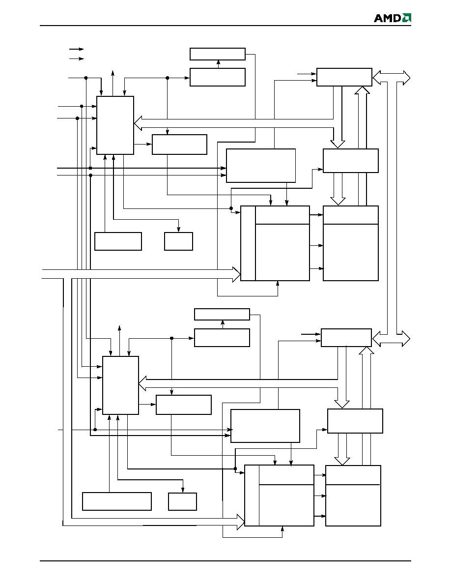
Block Diagram . . . . . . . . . . . . . . . . . . . . . . . . . . . . 5
Connection Diagram . . . . . . . . . . . . . . . . . . . . . . . . 6
Pin Description . . . . . . . . . . . . . . . . . . . . . . . . . . . . 7
Logic Symbol . . . . . . . . . . . . . . . . . . . . . . . . . . . . . 7
Ordering Information . . . . . . . . . . . . . . . . . . . . . . . 8
Device Bus Operations . . . . . . . . . . . . . . . . . . . . . . 9
Table 1. Am29LV652D Device Bus Operations ................................9
VersatileIO
TM (V
IO
) Control ....................................................... 9
Requirements for Reading Array Data ..................................... 9
Writing Commands/Command Sequences ............................ 10
Accelerated Program Operation .......................................... 10
Autoselect Functions ........................................................... 10
Standby Mode ........................................................................ 10
Automatic Sleep Mode ........................................................... 10
RESET#: Hardware Reset Pin ............................................... 10
Output Disable Mode .............................................................. 11
Table 2. Sector Address Table for CE# ..........................................11
Table 3. Sector Address Table for CE2# ........................................15
Autoselect Mode ..................................................................... 19
Table 4. Am29LV652D Autoselect Codes, (High Voltage Method) 19
Sector Group Protection and Unprotection ............................. 20
Table 5. Sector Group Protection/Unprotection Address Table .....20
Temporary Sector Group Unprotect ....................................... 21
Figure 1. Temporary Sector Group Unprotect Operation................ 21
Figure 2. In-System Sector Group Protect/Unprotect Algorithms ... 22
Hardware Data Protection ...................................................... 23
Low VCC Write Inhibit ......................................................... 23
Write Pulse "Glitch" Protection ............................................ 23
Logical Inhibit ...................................................................... 23
Power-Up Write Inhibit ......................................................... 23
Common Flash Memory Interface (CFI) . . . . . . . 23
Table 6. CFI Query Identification String .......................................... 23
System Interface String................................................................... 24
Table 8. Device Geometry Definition .............................................. 24
Table 9. Primary Vendor-Specific Extended Query ........................ 25
Command Definitions . . . . . . . . . . . . . . . . . . . . . 25
Reading Array Data ................................................................ 25
Reset Command ..................................................................... 26
Autoselect Command Sequence ............................................ 26
Byte Program Command Sequence ....................................... 26
Unlock Bypass Command Sequence .................................. 26
Figure 3. Program Operation .......................................................... 27
Chip Erase Command Sequence ........................................... 27
Sector Erase Command Sequence ........................................ 28
Erase Suspend/Erase Resume Commands ........................... 28
Figure 4. Erase Operation............................................................... 29
Table 10. Am29LV652D Command Definitions ............................. 30
Write Operation Status . . . . . . . . . . . . . . . . . . . . 31
DQ7: Data# Polling ................................................................. 31
Figure 5. Data# Polling Algorithm .................................................. 31
RY/BY#: Ready/Busy# ............................................................ 32
DQ6: Toggle Bit I .................................................................... 32
Figure 6. Toggle Bit Algorithm........................................................ 32
DQ2: Toggle Bit II ................................................................... 33
Reading Toggle Bits DQ6/DQ2 ............................................... 33
DQ5: Exceeded Timing Limits ................................................ 33
DQ3: Sector Erase Timer ....................................................... 33
Table 11. Write Operation Status ................................................... 34
Absolute Maximum Ratings . . . . . . . . . . . . . . . . 35
Operating Ranges . . . . . . . . . . . . . . . . . . . . . . . . 35
Figure 7. Maximum Negative Overshoot Waveform ..................... 35
Figure 8. Maximum Positive Overshoot Waveform....................... 35
DC Characteristics (for two Am29LV065 devices)
36
Figure 9. I
CC1
Current vs. Time (Showing Active and
Automatic Sleep Currents) ............................................................. 37
Figure 10. Typical I
CC1
vs. Frequency ............................................ 37
Test Conditions . . . . . . . . . . . . . . . . . . . . . . . . . . 38
Figure 11. Test Setup.................................................................... 38
Table 12. Test Specifications ......................................................... 38
Figure 12. Input Waveforms and Measurement Levels ................. 38
Key to Switching Waveforms. . . . . . . . . . . . . . . . 38
AC Characteristics . . . . . . . . . . . . . . . . . . . . . . . . 39
Read-Only Operations ........................................................... 39
Figure 13. Read Operation Timings ............................................... 39
Hardware Reset (RESET#) .................................................... 40
Figure 14. Reset Timings ............................................................... 40
Erase and Program Operations .............................................. 41
Figure 15. Program Operation Timings.......................................... 42
Figure 16. Accelerated Program Timing Diagram.......................... 42
Figure 17. Chip/Sector Erase Operation Timings .......................... 43
Figure 18. Data# Polling Timings (During Embedded Algorithms). 44
Figure 19. Toggle Bit Timings (During Embedded Algorithms)...... 45
Figure 20. DQ2 vs. DQ6................................................................. 45
Temporary Sector Unprotect .................................................. 46
Figure 21. Temporary Sector Group Unprotect Timing Diagram ... 46
Figure 22. Sector Group Protect and Unprotect Timing Diagram .. 47
Figure 23. Alternate CE# Controlled Write
(Erase/Program) Operation Timings .............................................. 49
Erase And Programming Performance . . . . . . . 50
Latchup Characteristics . . . . . . . . . . . . . . . . . . . . 50
Data Retention. . . . . . . . . . . . . . . . . . . . . . . . . . . . 50
Physical Dimensions . . . . . . . . . . . . . . . . . . . . . . 51
FSA063--63-Ball Fine-Pitch Ball Grid Array (FBGA) 11 x 12 mm
package .................................................................................. 51
Revision Summary . . . . . . . . . . . . . . . . . . . . . . . . 52

4
Am29LV652D
October 29, 2004
P R E L I M I N A R Y
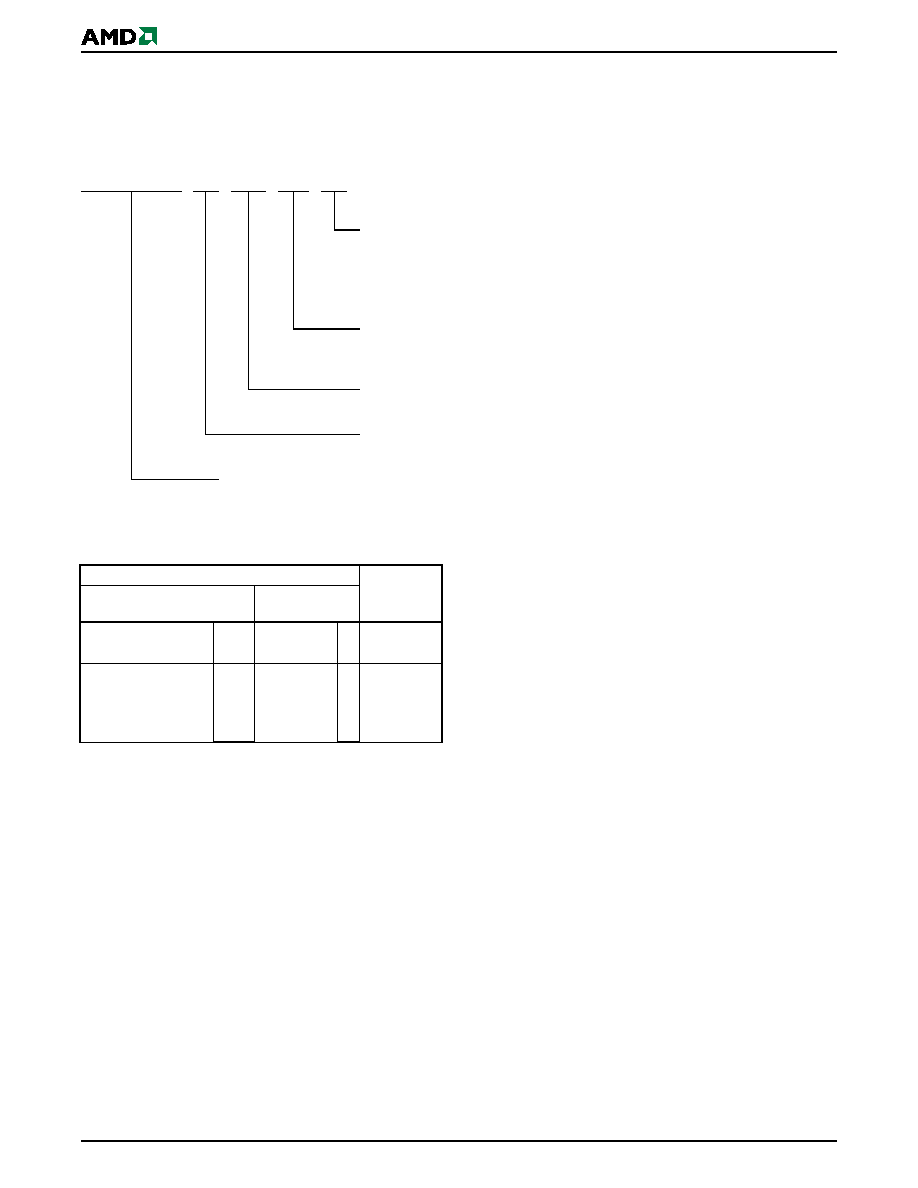
PRODUCT SELECTOR GUIDE
Note: See
"AC Characteristics" on page 39
for full specifications.
Part Number
Am29LV652D
Speed Option
Regulated Voltage Range: V
CC
= 3.0≠3.6 V
90R
12R
Max Access Time (ns)
90
120
CE# Access Time (ns)
90
120
OE# Access Time (ns)
35
50
October 29, 2004
Am29LV652D
5
P R E L I M I N A R Y
BLOCK DIAGRAM
Input/Output
Buffers
X-Decoder
Y-Decoder
Chip Enable
Output Enable
Logic
Erase Voltage
Generator
PGM Voltage
Generator
Timer
V
CC
Detector
State
Control
Command
Register
V
CC
V
SS
WE#
ACC
CE#
OE#
STB
STB
DQ0
≠
DQ7
Sector Switches
RY/BY#
RESET#
Data
Latch
Y-Gating
Cell Matrix
Addr
ess
L
a
tc
h
V
IO
Input/Output
Buffers
X-Decoder
Y-Decoder
Chip Enable
Output Enable
Logic
Erase Voltage
Generator
PGM Voltage
Generator
Timer
V
CC
Detector
State
Control
Command
Register
STB
STB
DQ0
≠
DQ7
Sector Switches
RY/BY#
Data
Latch
Y-Gating
Cell Matrix
Addre
s
s
La
tch
V
IO
A0≠A22
A0≠
A
22
A0≠A22
CE#2
6
Am29LV652D
October 29, 2004
P R E L I M I N A R Y
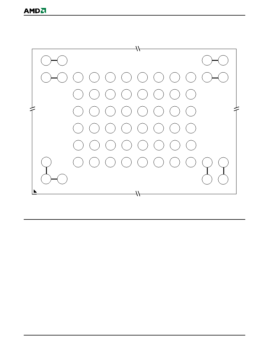
CONNECTION DIAGRAM
Special Handling Instructions for FBGA
Package
Special handling is required for Flash Memory products
in FBGA packages.
Flash memory devices in FBGA packages may be
damaged if exposed to ultrasonic cleaning methods.
The package and/or data integrity may be compromised
if the package body is exposed to temperatures above
150
∞C for prolonged periods of time.
C2
D2
C3
D3
E2
E3
F2
F3
G2
G3
H2
H3
J2
J3
K2
A3
A4
A2
A1
A0
CE#
OE#
V
SS
A7
A18
A6
A5
DQ0
NC
CE2#
DQ1
RY/BY#
ACC
NC
NC
DQ2
DQ3
V
IO
A21
WE#
RESET#
A22
NC
DQ5
NC
V
CC
DQ4
A9
A8
A11
A12
A19
A10
DQ6
DQ7
A14
A13
A15
A16
A17
NC
A20
V
SS
C4
D4
E4
A1
B1
A2
NC*
NC*
NC*
F4
G4
H4
J4
K4
C5
D5
E5
F5
G5
H5
J5
K5
C6
D6
E6
F6
G6
H6
J6
K6
C7
D7
E7
NC*
NC*
NC*
NC*
A7
B7
A8
B8
F7
G7
H7
J7
K7
NC*
NC*
NC*
NC*
L7
M7
L8
M8
K3
L1
L2
M1
NC*
NC*
NC*
NC*
M2
* Balls are shorted together via the substrate but not connected to the die.
63-Ball FBGA
Top View, Balls Facing
Down
October 29, 2004
Am29LV652D
7
P R E L I M I N A R Y
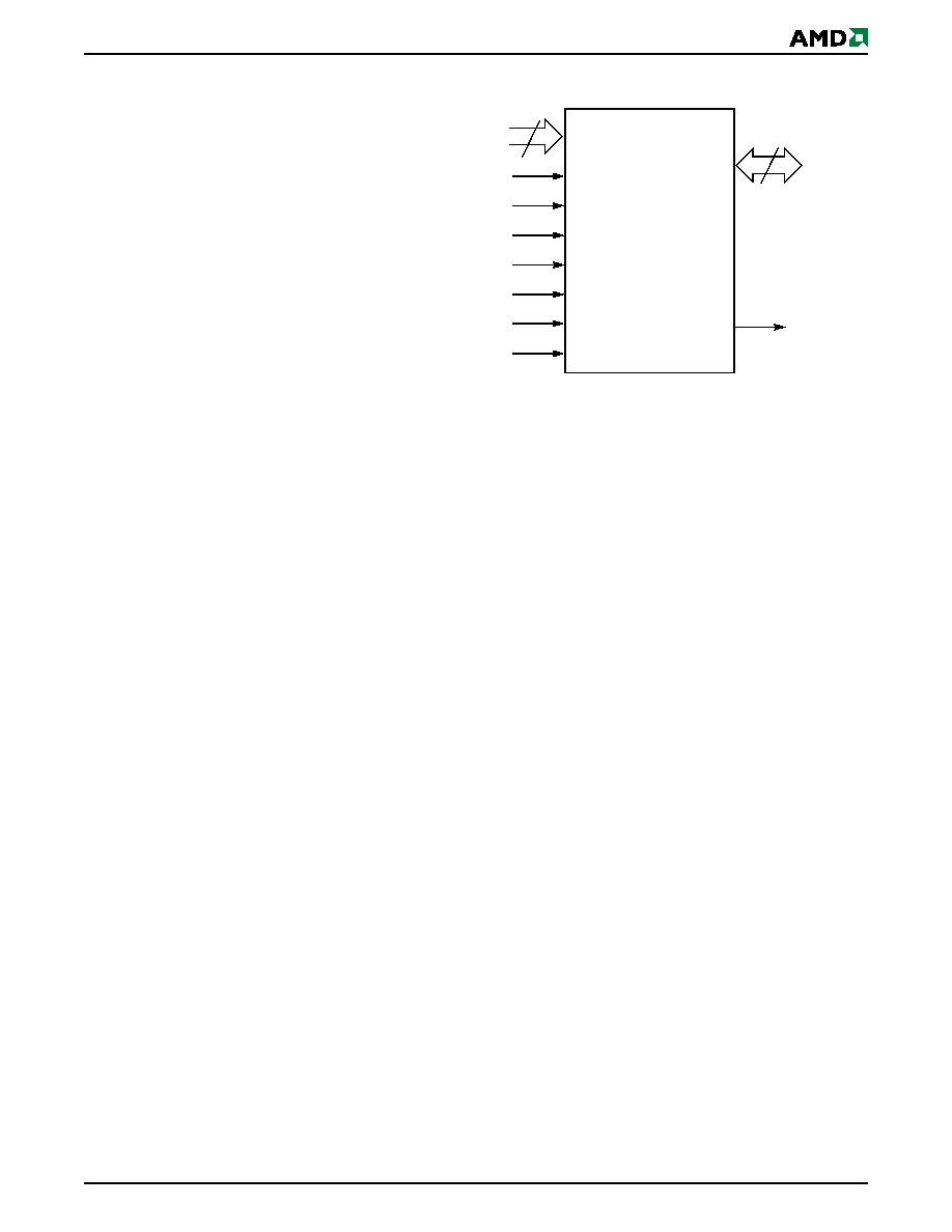
PIN DESCRIPTION
A0≠A22
= 23 Addresses inputs
DQ0≠DQ7
= 8 Data inputs/outputs
CE#
= Chip Enable input
CE2#
= Chip Enable input for second die
OE#
= Output Enable input
WE#
= Write Enable input
ACC
= Acceleration Input
RESET#
= Hardware Reset Pin input
RY/BY#
= Ready/Busy output
V
CC
= 3.0 volt-only single power supply
(see Product Selector Guide for
speed options and voltage
supply tolerances)
V
IO
= Output Buffer power
V
SS
= Device Ground
NC
= Pin Not Connected Internally
LOGIC SYMBOL
23
8
DQ0≠DQ7
A0≠A22
CE#
CE2#
OE#
ACC
RY/BY#
WE#
V
IO
RESET#
8
Am29LV652D
October 29, 2004
P R E L I M I N A R Y
ORDERING INFORMATION
Standard Products
AMD standard products are available in several packages and operating ranges. The order number (Valid Combination) is
formed by a combination of the following:
Valid Combinations
Valid Combinations list configurations planned to be sup-
ported in volume for this device. Consult the local AMD sales
office to confirm availability of specific valid combinations and
to check on newly released combinations.
Am29LV652D
U
90R
MA
I
TEMPERATURE RANGE
I =
Industrial
(≠40
∞
C to +85
∞
C)
E =
Extended
(≠55
∞
C to +125
∞
C)
F
=
Industrial (-40
o
C to +85
o
C) with Pb-free Package
K
=
Extended (-55
o
C to +125
o
C) with Pb-free Package
PACKAGE TYPE
MA
=
63-Ball Fine-Pitch Ball Grid Array (FBGA)
0.80 mm pitch, 11 x 12 mm package (FSA063)
SPEED OPTION
See Product Selector Guide and Valid Combinations
SECTOR ARCHITECTURE
U
=
Uniform sector device
DEVICE NUMBER/DESCRIPTION
Am29LV652D
128 Megabit (2 x 8 M x 8-Bit) CMOS Uniform Sector Flash Memory with VersatileIO
TM Control
3.0 Volt-only Read, Program, and Erase
Valid Combinations for FBGA Packages
Speed/
V
IO
Range
Order Number
Package
Marking
Am29LV652DU90R
MAF,
MAI
L652DU90R
F,
I
90 ns, V
IO
=
3.0 V ≠ 5.0 V
Am29LV652DU12R
MAI,
MAE
MAF,
MAK
L652DU12R
I,
E,
F,
K
120 ns, V
IO
=
3.0 V ≠ 5.0 V
October 29, 2004
Am29LV652D
9
P R E L I M I N A R Y
DEVICE BUS OPERATIONS
This section describes the requirements and use of
the device bus operations, which are initiated through
the internal command register. The command register
itself does not occupy any addressable memory loca-
tion. The register is a latch used to store the com-
mands, along with the address and data information
needed to execute the command. The contents of the
register serve as inputs to the internal state machine.
The state machine outputs dictate the function of the
device.
Table 1
lists the device bus operations, the in-
puts and control levels they require, and the resulting
output. The following subsections describe each of
these operations in further detail.
Table 1. Am29LV652D Device Bus Operations
Legend: L = Logic Low = V
IL
, H = Logic High = V
IH
, V
ID
= 8.5≠12.5
V, V
HH
= 11.5≠12.5
V, X = Don't Care, SA = Sector Address,
A
IN
= Address In, D
IN
= Data In, D
OUT
= Data Out
Notes:
1. CE# can be replaced with CE2# when referring to the second die in the package. CE# and CE2# must not both be driven at
the same time.
2. Addresses are A22:A0. Sector addresses are A22:A16.
3. D
IN
or D
OUT
as required by command sequence, data polling, or sector protect algorithm (see
Figure 2
).
4. The sector protect and sector unprotect functions may also be implemented via programming equipment. See the "Sector Group
Protection and Unprotection" section.
5. All sectors are unprotected when shipped from the factory.
VersatileIO
TM (V
IO
) Control
The VersatileIO (V
IO
) control allows the host system to
set the voltage levels that the device generates at its
data outputs and the voltages tolerated at its data in-
puts to the same voltage level that is asserted on V
IO
.
This allows the device to operate in a 3 V or 5 V sys-
tem environment as required. For voltage levels below
3 V, contact an AMD representative for more informa-
tion.
For example, a V
I/O
of 4.5≠5.0 volts allows for I/O at
the 5 volt level, driving and receiving signals to and
from other 5 V devices on the same data bus.
Requirements for Reading Array Data
To read array data from the outputs, the system must
drive CE# or CE2# and OE# to V
IL
. CE# or CE2# is the
power control and selects the device. OE# is the out-
put control and gates array data to the outputs. WE#
should remain at V
IH
.
The internal state machine is set for reading array data
upon device power-up, or after a hardware reset. This
ensures that no spurious alteration of the memory
content occurs during the power transition. No com-
mand is necessary in this mode to obtain array data.
Standard microprocessor read cycles that assert valid
addresses on the device address inputs produce valid
data on the device data outputs. The device remains
Operation
CE#
(Note 1)
OE#
WE#
RESET#
ACC
Addresses
(Note 2)
DQ0≠DQ7
Read
L
L
H
H
X
A
IN
D
OUT
Write (Program/Erase)
L
H
L
H
X
A
IN
(Note 3)
Accelerated Program
L
H
L
H
V
HH
A
IN
(Note 3)
Standby
V
CC
± 0.3 V
X
X
V
CC
± 0.3 V
H
X
High-Z
Output Disable
L
H
H
H
X
X
High-Z
Reset
X
X
X
L
X
X
High-Z
Sector Group Protect (Note 4)
L
H
L
V
ID
X
SA, A6 = L,
A1 = H, A0 = L
(Note 3)
Sector Group Unprotect
(Note 4)
L
H
L
V
ID
X
SA, A6 = H,
A1 = H, A0 = L
(Note 3)
Temporary Sector Group
Unprotect
X
X
X
V
ID
X
A
IN
(Note 3)

10
Am29LV652D
October 29, 2004
P R E L I M I N A R Y
enabled for read access until the command register
contents are altered.
See "VersatileIO
TM (V
IO
) Control" for more information.
Refer to the AC
"Read-Only Operations" on page 39
table for timing specifications and to
Figure 13, on
page 39
for the timing diagram. I
CC1
in the DC Charac-
teristics table represents the active current specifica-
tion for reading array data.
Writing Commands/Command Sequences
To write a command or command sequence (which in-
cludes programming data to the device and erasing
sectors of memory), the system must drive WE# and
CE# (or CE2#) to V
IL
, and OE# to V
IH
.
The device features an Unlock Bypass mode to facili-
tate faster programming. Once the device enters the
Unlock Bypass mode, only two write cycles are re-
quired to program a byte, instead of four. The
"Byte
Program Command Sequence" on page 26
section
contains details on programming data to the device
using both standard and Unlock Bypass command se-
quences.
An erase operation can erase one sector, multiple sec-
tors, or the entire device.
Table 2, on page 11
indicates
the address space that each sector occupies.
I
CC2
in the DC Characteristics table represents the ac-
tive current specification for the write mode. The AC
Characteristics section contains timing specification
tables and timing diagrams for write operations.
Accelerated Program Operation
The device offers accelerated program operations
through the ACC function. This function is primarily in-
tended to allow faster manufacturing throughput dur-
ing system production.
If the system asserts V
HH
on ACC, the device automat-
ically enters the aforementioned Unlock Bypass mode,
temporarily unprotects any protected sectors, and
uses the higher voltage to reduce the time required for
program operations. The system would use a two-cy-
cle program command sequence as required by the
Unlock Bypass mode. Removing V
HH
from ACC re-
turns the device to normal operation. Note that ACC
must not be at V
HH
for operations other than acceler-
ated programming, or device damage may result.
Autoselect Functions
If the system writes the autoselect command se-
quence, the device enters the autoselect mode. The
system can then read autoselect codes from the inter-
nal register (which is separate from the memory array)
on DQ7≠DQ0. Standard read cycle timings apply in
this mode. Refer to the
"Autoselect Mode" on page 19
and
"Autoselect Command Sequence" on page 26
sections for more information.
Standby Mode
When the system is not reading or writing to the de-
vice, it can place the device in the standby mode. In
this mode, current consumption is greatly reduced,
and the outputs are placed in the high impedance
state, independent of the OE# input.
The device enters the CMOS standby mode when the
CE#, CE2#, and RESET# are all held at V
CC
± 0.3 V.
(Note that this is a more restricted voltage range than
V
IH
.) If CE#, CE2#, and RESET# are held at V
IH
, but
not within V
CC
± 0.3 V, the device is in the standby
mode, but the standby current is greater. The device
requires standard access time (t
CE
) for read access
when the device is in either of these standby modes,
before it is ready to read data.
If the device is deselected during erasure or program-
ming, the device draws active current until the
operation is completed.
I
CC3
in the DC Characteristics (for two Am29LV065 de-
vices) table represents the standby current specifica-
tion.
Automatic Sleep Mode
The automatic sleep mode minimizes Flash device en-
ergy consumption. The device automatically enables
this mode when addresses remain stable for t
ACC
+
30 ns. The automatic sleep mode is independent of
the CE#, CE2#, WE#, and OE# control signals. Stan-
dard address access timings provide new data when
addresses are changed. While in sleep mode, output
data is latched and always available to the system.
I
CC4
in the DC Characteristics (for two Am29LV065 de-
vices) table represents the automatic sleep mode cur-
rent specification.
RESET#: Hardware Reset Pin
RESET# provides a hardware method of resetting the
device to reading array data. When RESET# is driven
low for at least a period of t
RP
, the device immediately
terminates any operation in progress, tristates all out-
puts, and ignores all read/write commands for the du-
ration of the RESET# pulse. The device also resets
the internal state machine to reading array data. The
operation that was interrupted should be reinitiated
once the device is ready to accept another command
sequence, to ensure data integrity.
Current is reduced for the duration of the RESET#
pulse. When RESET# is held at V
SS
± 0.3 V, the device
draws CMOS standby current (I
CC4
). If RESET# is held
at V
IL,
but not within V
SS
± 0.3 V, the standby current is
greater.
RESET# may be tied to the system reset circuitry. A
system reset would thus also reset the Flash memory,

October 29, 2004
Am29LV652D
11
P R E L I M I N A R Y
enabling the system to read the boot-up firmware from
the Flash memory.
If RESET# is asserted during a program or erase op-
eration, RY/BY# remains a "0" (busy) until the internal
reset operation is complete, which requires a time of
t
READY
(during Embedded Algorithms). The system can
thus monitor RY/BY# to determine whether the reset
operation is complete. If RESET# is asserted when a
program or erase operation is not executing (RY/BY#
is "1"), the reset operation is completed within a time
of t
READY
(not during Embedded Algorithms). The sys-
tem can read data t
RH
after RESET# returns to V
IH
.
Refer to the
"AC Characteristics" on page 39
tables for
RESET# parameters and to
Figure 14, on page 40
for
the timing diagram.
Output Disable Mode
When the OE# input is at V
IH
, output from the device is
disabled. The outputs are placed in the high
impedance state.
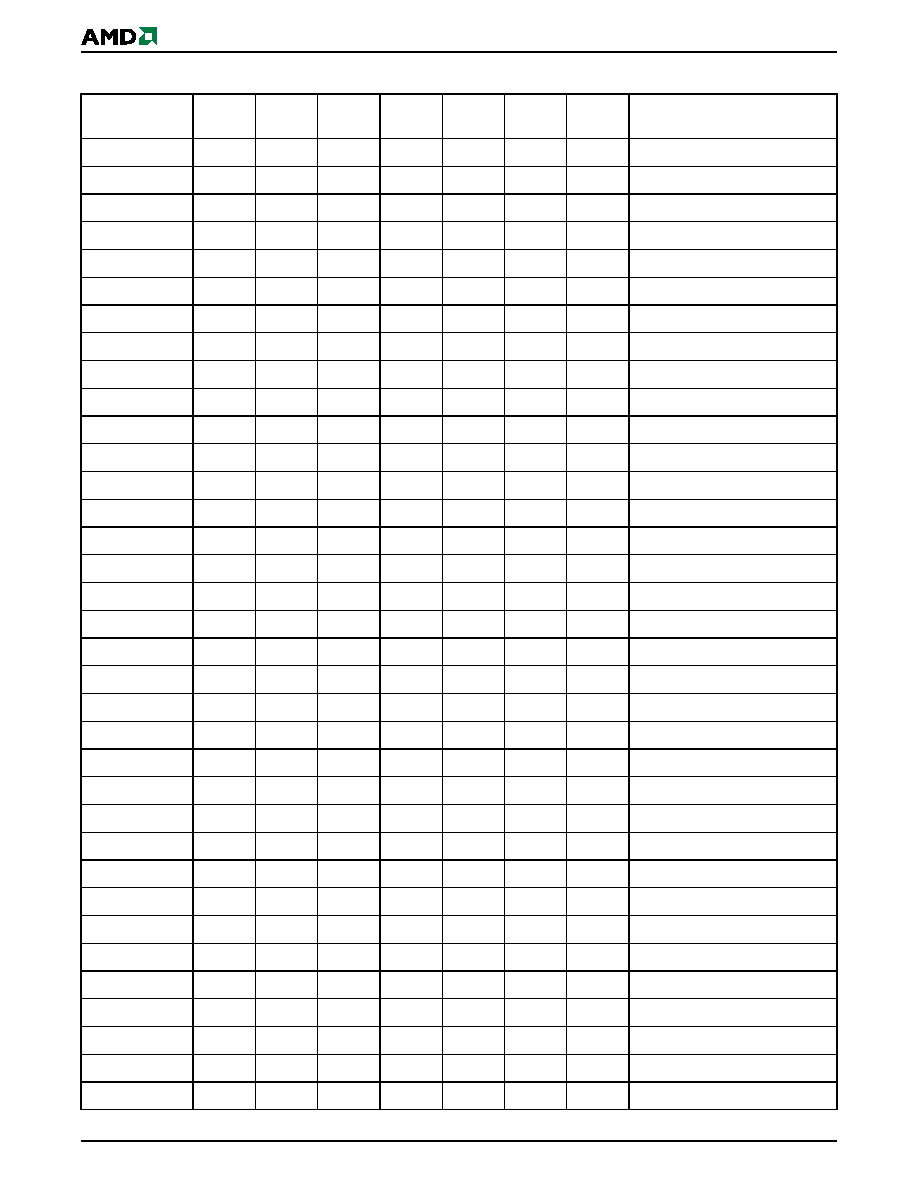
Table 2. Sector Address Table for CE# (Sheet 1 of 4)
Sector
A22
A21
A20
A19
A18
A17
A16
8-bit Address Range
(in hexadecimal)
SA0
0
0
0
0
0
0
0
000000≠00FFFF
SA1
0
0
0
0
0
0
1
010000≠01FFFF
SA2
0
0
0
0
0
1
0
020000≠02FFFF
SA3
0
0
0
0
0
1
1
030000≠03FFFF
SA4
0
0
0
0
1
0
0
040000≠04FFFF
SA5
0
0
0
0
1
0
1
050000≠05FFFF
SA6
0
0
0
0
1
1
0
060000≠06FFFF
SA7
0
0
0
0
1
1
1
070000≠07FFFF
SA8
0
0
0
1
0
0
0
080000≠08FFFF
SA9
0
0
0
1
0
0
1
090000≠09FFFF
SA10
0
0
0
1
0
1
0
0A0000≠0AFFFF
SA11
0
0
0
1
0
1
1
0B0000≠0BFFFF
SA12
0
0
0
1
1
0
0
0C0000≠0CFFFF
SA13
0
0
0
1
1
0
1
0D0000≠0DFFFF
SA14
0
0
0
1
1
1
0
0E0000≠0EFFFF
SA15
0
0
0
1
1
1
1
0F0000≠0FFFFF
SA16
0
0
1
0
0
0
0
100000≠10FFFF
SA17
0
0
1
0
0
0
1
110000≠11FFFF
SA18
0
0
1
0
0
1
0
120000≠12FFFF
SA19
0
0
1
0
0
1
1
130000≠13FFFF
SA20
0
0
1
0
1
0
0
140000≠14FFFF
SA21
0
0
1
0
1
0
1
150000≠15FFFF
SA22
0
0
1
0
1
1
0
160000≠16FFFF
SA23
0
0
1
0
1
1
1
170000≠17FFFF
SA24
0
0
1
1
0
0
0
180000≠18FFFF
SA25
0
0
1
1
0
0
1
190000≠19FFFF
SA26
0
0
1
1
0
1
0
1A0000≠1AFFFF

12
Am29LV652D
October 29, 2004
P R E L I M I N A R Y
SA27
0
0
1
1
0
1
1
1B0000≠1BFFFF
SA28
0
0
1
1
1
0
0
1C0000≠1CFFFF
SA29
0
0
1
1
1
0
1
1D0000≠1DFFFF
SA30
0
0
1
1
1
1
0
1E0000≠1EFFFF
SA31
0
0
1
1
1
1
1
1F0000≠1FFFFF
SA32
0
1
0
0
0
0
0
200000≠20FFFF
SA33
0
1
0
0
0
0
1
210000≠21FFFF
SA34
0
1
0
0
0
1
0
220000≠22FFFF
SA35
0
1
0
0
0
1
1
230000≠23FFFF
SA36
0
1
0
0
1
0
0
240000≠24FFFF
SA37
0
1
0
0
1
0
1
250000≠25FFFF
SA38
0
1
0
0
1
1
0
260000≠26FFFF
SA39
0
1
0
0
1
1
1
270000≠27FFFF
SA40
0
1
0
1
0
0
0
280000≠28FFFF
SA41
0
1
0
1
0
0
1
290000≠29FFFF
SA42
0
1
0
1
0
1
0
2A0000≠2AFFFF
SA43
0
1
0
1
0
1
1
2B0000≠2BFFFF
SA44
0
1
0
1
1
0
0
2C0000≠2CFFFF
SA45
0
1
0
1
1
0
1
2D0000≠2DFFFF
SA46
0
1
0
1
1
1
0
2E0000≠2EFFFF
SA47
0
1
0
1
1
1
1
2F0000≠2FFFFF
SA48
0
1
1
0
0
0
0
300000≠30FFFF
SA49
0
1
1
0
0
0
1
310000≠31FFFF
SA50
0
1
1
0
0
1
0
320000≠32FFFF
SA51
0
1
1
0
0
1
1
330000≠33FFFF
SA52
0
1
1
0
1
0
0
340000≠34FFFF
SA53
0
1
1
0
1
0
1
350000≠35FFFF
SA54
0
1
1
0
1
1
0
360000≠36FFFF
SA55
0
1
1
0
1
1
1
370000≠37FFFF
SA56
0
1
1
1
0
0
0
380000≠38FFFF
SA57
0
1
1
1
0
0
1
390000≠39FFFF
SA58
0
1
1
1
0
1
0
3A0000≠3AFFFF
SA59
0
1
1
1
0
1
1
3B0000≠3BFFFF
SA60
0
1
1
1
1
0
0
3C0000≠3CFFFF
SA61
0
1
1
1
1
0
1
3D0000≠3DFFFF
Table 2. Sector Address Table for CE# (Sheet 2 of 4)
Sector
A22
A21
A20
A19
A18
A17
A16
8-bit Address Range
(in hexadecimal)
October 29, 2004
Am29LV652D
13
P R E L I M I N A R Y
SA62
0
1
1
1
1
1
0
3E0000≠3EFFFF
SA63
0
1
1
1
1
1
1
3F0000≠3FFFFF
SA64
1
0
0
0
0
0
0
400000≠40FFFF
SA65
1
0
0
0
0
0
1
410000≠41FFFF
SA66
1
0
0
0
0
1
0
420000≠42FFFF
SA67
1
0
0
0
0
1
1
430000≠43FFFF
SA68
1
0
0
0
1
0
0
440000≠44FFFF
SA69
1
0
0
0
1
0
1
450000≠45FFFF
SA70
1
0
0
0
1
1
0
460000≠46FFFF
SA71
1
0
0
0
1
1
1
470000≠47FFFF
SA72
1
0
0
1
0
0
0
480000≠48FFFF
SA73
1
0
0
1
0
0
1
490000≠49FFFF
SA74
1
0
0
1
0
1
0
4A0000≠4AFFFF
SA75
1
0
0
1
0
1
1
4B0000≠4BFFFF
SA76
1
0
0
1
1
0
0
4C0000≠4CFFFF
SA77
1
0
0
1
1
0
1
4D0000≠4DFFFF
SA78
1
0
0
1
1
1
0
4E0000≠4EFFFF
SA79
1
0
0
1
1
1
1
4F0000≠4FFFFF
SA80
1
0
1
0
0
0
0
500000≠50FFFF
SA81
1
0
1
0
0
0
1
510000≠51FFFF
SA82
1
0
1
0
0
1
0
520000≠52FFFF
SA83
1
0
1
0
0
1
1
530000≠53FFFF
SA84
1
0
1
0
1
0
0
540000≠54FFFF
SA85
1
0
1
0
1
0
1
550000≠55FFFF
SA86
1
0
1
0
1
1
0
560000≠56FFFF
SA87
1
0
1
0
1
1
1
570000≠57FFFF
SA88
1
0
1
1
0
0
0
580000≠58FFFF
SA89
1
0
1
1
0
0
1
590000≠59FFFF
SA90
1
0
1
1
0
1
0
5A0000≠5AFFFF
SA91
1
0
1
1
0
1
1
5B0000≠5BFFFF
SA92
1
0
1
1
1
0
0
5C0000≠5CFFFF
SA93
1
0
1
1
1
0
1
5D0000≠5DFFFF
SA94
1
0
1
1
1
1
0
5E0000≠5EFFFF
SA95
1
0
1
1
1
1
1
5F0000≠5FFFFF
SA96
1
1
0
0
0
0
0
600000≠60FFFF
Table 2. Sector Address Table for CE# (Sheet 3 of 4)
Sector
A22
A21
A20
A19
A18
A17
A16
8-bit Address Range
(in hexadecimal)
14
Am29LV652D
October 29, 2004
P R E L I M I N A R Y
Note: All sectors are 64 Kbytes in size.
SA97
1
1
0
0
0
0
1
610000≠61FFFF
SA98
1
1
0
0
0
1
0
620000≠62FFFF
SA99
1
1
0
0
0
1
1
630000≠63FFFF
SA100
1
1
0
0
1
0
0
640000≠64FFFF
SA101
1
1
0
0
1
0
1
650000≠65FFFF
SA102
1
1
0
0
1
1
0
660000≠66FFFF
SA103
1
1
0
0
1
1
1
670000≠67FFFF
SA104
1
1
0
1
0
0
0
680000≠68FFFF
SA105
1
1
0
1
0
0
1
690000≠69FFFF
SA106
1
1
0
1
0
1
0
6A0000≠6AFFFF
SA107
1
1
0
1
0
1
1
6B0000≠6BFFFF
SA108
1
1
0
1
1
0
0
6C0000≠6CFFFF
SA109
1
1
0
1
1
0
1
6D0000≠6DFFFF
SA110
1
1
0
1
1
1
0
6E0000≠6EFFFF
SA111
1
1
0
1
1
1
1
6F0000≠6FFFFF
SA112
1
1
1
0
0
0
0
700000≠70FFFF
SA113
1
1
1
0
0
0
1
710000≠71FFFF
SA114
1
1
1
0
0
1
0
720000≠72FFFF
SA115
1
1
1
0
0
1
1
730000≠73FFFF
SA116
1
1
1
0
1
0
0
740000≠74FFFF
SA117
1
1
1
0
1
0
1
750000≠75FFFF
SA118
1
1
1
0
1
1
0
760000≠76FFFF
SA119
1
1
1
0
1
1
1
770000≠77FFFF
SA120
1
1
1
1
0
0
0
780000≠78FFFF
SA121
1
1
1
1
0
0
1
790000≠79FFFF
SA122
1
1
1
1
0
1
0
7A0000≠7AFFFF
SA123
1
1
1
1
0
1
1
7B0000≠7BFFFF
SA124
1
1
1
1
1
0
0
7C0000≠7CFFFF
SA125
1
1
1
1
1
0
1
7D0000≠7DFFFF
SA126
1
1
1
1
1
1
0
7E0000≠7EFFFF
SA127
1
1
1
1
1
1
1
7F0000≠7FFFFF
Table 2. Sector Address Table for CE# (Sheet 4 of 4)
Sector
A22
A21
A20
A19
A18
A17
A16
8-bit Address Range
(in hexadecimal)
October 29, 2004
Am29LV652D
15
P R E L I M I N A R Y
Table 3. Sector Address Table for CE2# (Sheet 1 of 4)
Sector
A22
A21
A20
A19
A18
A17
A16
8-bit Address Range
(in hexadecimal)
SA0
0
0
0
0
0
0
0
000000≠00FFFF
SA1
0
0
0
0
0
0
1
010000≠01FFFF
SA2
0
0
0
0
0
1
0
020000≠02FFFF
SA3
0
0
0
0
0
1
1
030000≠03FFFF
SA4
0
0
0
0
1
0
0
040000≠04FFFF
SA5
0
0
0
0
1
0
1
050000≠05FFFF
SA6
0
0
0
0
1
1
0
060000≠06FFFF
SA7
0
0
0
0
1
1
1
070000≠07FFFF
SA8
0
0
0
1
0
0
0
080000≠08FFFF
SA9
0
0
0
1
0
0
1
090000≠09FFFF
SA10
0
0
0
1
0
1
0
0A0000≠0AFFFF
SA11
0
0
0
1
0
1
1
0B0000≠0BFFFF
SA12
0
0
0
1
1
0
0
0C0000≠0CFFFF
SA13
0
0
0
1
1
0
1
0D0000≠0DFFFF
SA14
0
0
0
1
1
1
0
0E0000≠0EFFFF
SA15
0
0
0
1
1
1
1
0F0000≠0FFFFF
SA16
0
0
1
0
0
0
0
100000≠10FFFF
SA17
0
0
1
0
0
0
1
110000≠11FFFF
SA18
0
0
1
0
0
1
0
120000≠12FFFF
SA19
0
0
1
0
0
1
1
130000≠13FFFF
SA20
0
0
1
0
1
0
0
140000≠14FFFF
SA21
0
0
1
0
1
0
1
150000≠15FFFF
SA22
0
0
1
0
1
1
0
160000≠16FFFF
SA23
0
0
1
0
1
1
1
170000≠17FFFF
SA24
0
0
1
1
0
0
0
180000≠18FFFF
SA25
0
0
1
1
0
0
1
190000≠19FFFF
SA26
0
0
1
1
0
1
0
1A0000≠1AFFFF
SA27
0
0
1
1
0
1
1
1B0000≠1BFFFF
SA28
0
0
1
1
1
0
0
1C0000≠1CFFFF
SA29
0
0
1
1
1
0
1
1D0000≠1DFFFF
SA30
0
0
1
1
1
1
0
1E0000≠1EFFFF
SA31
0
0
1
1
1
1
1
1F0000≠1FFFFF
SA32
0
1
0
0
0
0
0
200000≠20FFFF
SA33
0
1
0
0
0
0
1
210000≠21FFFF
16
Am29LV652D
October 29, 2004
P R E L I M I N A R Y
SA34
0
1
0
0
0
1
0
220000≠22FFFF
SA35
0
1
0
0
0
1
1
230000≠23FFFF
SA36
0
1
0
0
1
0
0
240000≠24FFFF
SA37
0
1
0
0
1
0
1
250000≠25FFFF
SA38
0
1
0
0
1
1
0
260000≠26FFFF
SA39
0
1
0
0
1
1
1
270000≠27FFFF
SA40
0
1
0
1
0
0
0
280000≠28FFFF
SA41
0
1
0
1
0
0
1
290000≠29FFFF
SA42
0
1
0
1
0
1
0
2A0000≠2AFFFF
SA43
0
1
0
1
0
1
1
2B0000≠2BFFFF
SA44
0
1
0
1
1
0
0
2C0000≠2CFFFF
SA45
0
1
0
1
1
0
1
2D0000≠2DFFFF
SA46
0
1
0
1
1
1
0
2E0000≠2EFFFF
SA47
0
1
0
1
1
1
1
2F0000≠2FFFFF
SA48
0
1
1
0
0
0
0
300000≠30FFFF
SA49
0
1
1
0
0
0
1
310000≠31FFFF
SA50
0
1
1
0
0
1
0
320000≠32FFFF
SA51
0
1
1
0
0
1
1
330000≠33FFFF
SA52
0
1
1
0
1
0
0
340000≠34FFFF
SA53
0
1
1
0
1
0
1
350000≠35FFFF
SA54
0
1
1
0
1
1
0
360000≠36FFFF
SA55
0
1
1
0
1
1
1
370000≠37FFFF
SA56
0
1
1
1
0
0
0
380000≠38FFFF
SA57
0
1
1
1
0
0
1
390000≠39FFFF
SA58
0
1
1
1
0
1
0
3A0000≠3AFFFF
SA59
0
1
1
1
0
1
1
3B0000≠3BFFFF
SA60
0
1
1
1
1
0
0
3C0000≠3CFFFF
SA61
0
1
1
1
1
0
1
3D0000≠3DFFFF
SA62
0
1
1
1
1
1
0
3E0000≠3EFFFF
SA63
0
1
1
1
1
1
1
3F0000≠3FFFFF
SA64
1
0
0
0
0
0
0
400000≠40FFFF
SA65
1
0
0
0
0
0
1
410000≠41FFFF
SA66
1
0
0
0
0
1
0
420000≠42FFFF
SA67
1
0
0
0
0
1
1
430000≠43FFFF
SA68
1
0
0
0
1
0
0
440000≠44FFFF
Table 3. Sector Address Table for CE2# (Sheet 2 of 4)
Sector
A22
A21
A20
A19
A18
A17
A16
8-bit Address Range
(in hexadecimal)

October 29, 2004
Am29LV652D
17
P R E L I M I N A R Y
SA69
1
0
0
0
1
0
1
450000≠45FFFF
SA70
1
0
0
0
1
1
0
460000≠46FFFF
SA71
1
0
0
0
1
1
1
470000≠47FFFF
SA72
1
0
0
1
0
0
0
480000≠48FFFF
SA73
1
0
0
1
0
0
1
490000≠49FFFF
SA74
1
0
0
1
0
1
0
4A0000≠4AFFFF
SA75
1
0
0
1
0
1
1
4B0000≠4BFFFF
SA76
1
0
0
1
1
0
0
4C0000≠4CFFFF
SA77
1
0
0
1
1
0
1
4D0000≠4DFFFF
SA78
1
0
0
1
1
1
0
4E0000≠4EFFFF
SA79
1
0
0
1
1
1
1
4F0000≠4FFFFF
SA80
1
0
1
0
0
0
0
500000≠50FFFF
SA81
1
0
1
0
0
0
1
510000≠51FFFF
SA82
1
0
1
0
0
1
0
520000≠52FFFF
SA83
1
0
1
0
0
1
1
530000≠53FFFF
SA84
1
0
1
0
1
0
0
540000≠54FFFF
SA85
1
0
1
0
1
0
1
550000≠55FFFF
SA86
1
0
1
0
1
1
0
560000≠56FFFF
SA87
1
0
1
0
1
1
1
570000≠57FFFF
SA88
1
0
1
1
0
0
0
580000≠58FFFF
SA89
1
0
1
1
0
0
1
590000≠59FFFF
SA90
1
0
1
1
0
1
0
5A0000≠5AFFFF
SA91
1
0
1
1
0
1
1
5B0000≠5BFFFF
SA92
1
0
1
1
1
0
0
5C0000≠5CFFFF
SA93
1
0
1
1
1
0
1
5D0000≠5DFFFF
SA94
1
0
1
1
1
1
0
5E0000≠5EFFFF
SA95
1
0
1
1
1
1
1
5F0000≠5FFFFF
SA96
1
1
0
0
0
0
0
600000≠60FFFF
SA97
1
1
0
0
0
0
1
610000≠61FFFF
SA98
1
1
0
0
0
1
0
620000≠62FFFF
SA99
1
1
0
0
0
1
1
630000≠63FFFF
SA100
1
1
0
0
1
0
0
640000≠64FFFF
SA101
1
1
0
0
1
0
1
650000≠65FFFF
SA102
1
1
0
0
1
1
0
660000≠66FFFF
SA103
1
1
0
0
1
1
1
670000≠67FFFF
Table 3. Sector Address Table for CE2# (Sheet 3 of 4)
Sector
A22
A21
A20
A19
A18
A17
A16
8-bit Address Range
(in hexadecimal)

18
Am29LV652D
October 29, 2004
P R E L I M I N A R Y
Note: All sectors are 64 Kbytes in size.
SA104
1
1
0
1
0
0
0
680000≠68FFFF
SA105
1
1
0
1
0
0
1
690000≠69FFFF
SA106
1
1
0
1
0
1
0
6A0000≠6AFFFF
SA107
1
1
0
1
0
1
1
6B0000≠6BFFFF
SA108
1
1
0
1
1
0
0
6C0000≠6CFFFF
SA109
1
1
0
1
1
0
1
6D0000≠6DFFFF
SA110
1
1
0
1
1
1
0
6E0000≠6EFFFF
SA111
1
1
0
1
1
1
1
6F0000≠6FFFFF
SA112
1
1
1
0
0
0
0
700000≠70FFFF
SA113
1
1
1
0
0
0
1
710000≠71FFFF
SA114
1
1
1
0
0
1
0
720000≠72FFFF
SA115
1
1
1
0
0
1
1
730000≠73FFFF
SA116
1
1
1
0
1
0
0
740000≠74FFFF
SA117
1
1
1
0
1
0
1
750000≠75FFFF
SA118
1
1
1
0
1
1
0
760000≠76FFFF
SA119
1
1
1
0
1
1
1
770000≠77FFFF
SA120
1
1
1
1
0
0
0
780000≠78FFFF
SA121
1
1
1
1
0
0
1
790000≠79FFFF
SA122
1
1
1
1
0
1
0
7A0000≠7AFFFF
SA123
1
1
1
1
0
1
1
7B0000≠7BFFFF
SA124
1
1
1
1
1
0
0
7C0000≠7CFFFF
SA125
1
1
1
1
1
0
1
7D0000≠7DFFFF
SA126
1
1
1
1
1
1
0
7E0000≠7EFFFF
SA127
1
1
1
1
1
1
1
7F0000≠7FFFFF
Table 3. Sector Address Table for CE2# (Sheet 4 of 4)
Sector
A22
A21
A20
A19
A18
A17
A16
8-bit Address Range
(in hexadecimal)
October 29, 2004
Am29LV652D
19
P R E L I M I N A R Y
Autoselect Mode
The autoselect mode provides manufacturer and de-
vice identification, and sector protection verification,
through identifier codes output on DQ7≠DQ0. This
mode is primarily intended for programming equip-
ment to automatically match a device to be pro-
grammed with its corresponding programming
algorithm. However, the autoselect codes can also be
accessed in-system through the command register.
When using programming equipment, the autoselect
mode requires V
ID
(8.5 V to 12.5 V) on address A9.
Addresses A6, A1, and A0 must be as shown in
Table 4, on page 19
. In addition, when verifying sector
protection, the sector address must appear on the ap-
propriate highest order address bits (see
Table 2, on
page 11
and
Table 3, on page 15
).
Table 4
shows the
remaining address bits that are don't care. When all
necessary bits have been set as required, the pro-
gramming equipment may then read the correspond-
ing identifier code on DQ7≠DQ0.
To access the autoselect codes in-system, the host
system can issue the autoselect command via the
command register, as shown in
Table 10, on page 30
.
This method does not require V
ID
. Refer to the
"Au-
toselect Command Sequence" on page 26
section for
more information.
Table 4. Am29LV652D Autoselect Codes, (High Voltage Method)
Legend: L = Logic Low = V
IL
, H = Logic High = V
IH
, SA = Sector Address, X = Don't care.
Notes:
1. CE# can be replaced with CE2# when referring to the second die in the package.
2. The device ID's used for the Am29LV652 are the same as the Am29LV065, because the Am29LV652 uses two Am29LV065
dice and appears to the system as two Am29LV065 devices.
Description
CE# OE# WE#
A22
to
A16
A15
to
A10
A9
A8
to
A7
A6
A5
to
A2
A1
A0
DQ7 to DQ0
Manufacturer ID: AMD
L
L
H
X
X
V
ID
X
L
X
L
L
01h
Device ID: Am29LV652D
L
L
H
X
X
V
ID
X
L
X
L
H
93h
Sector Protection
Verification
L
L
H
SA
X
V
ID
X
L
X
H
L
01h (protected),
00h (unprotected)

20
Am29LV652D
October 29, 2004
P R E L I M I N A R Y
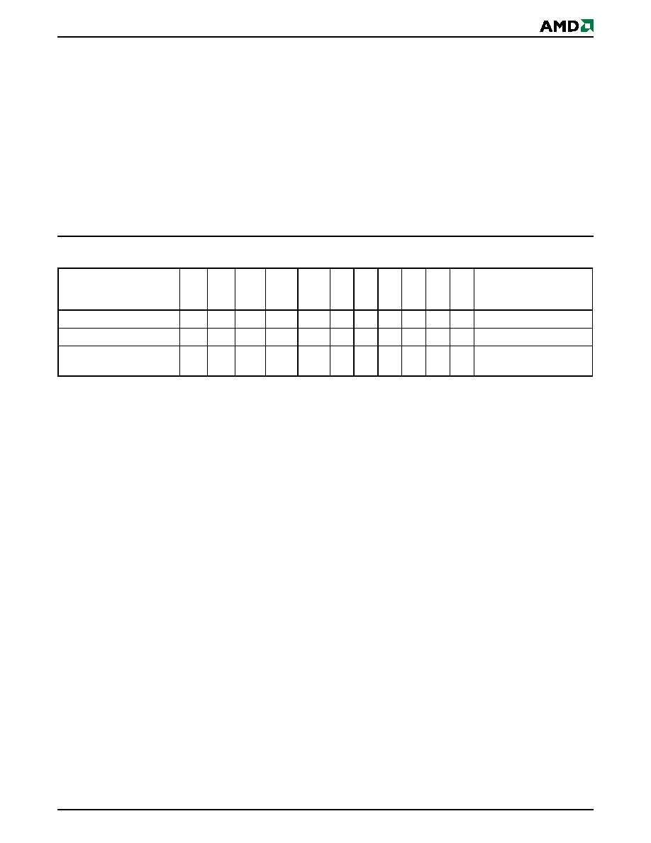
Sector Group Protection and
Unprotection
The hardware sector group protection feature disables
both program and erase operations in any sector
group. In this device, a sector group consists of four
adjacent sectors that are protected or unprotected at
the same time (see
Table 5
). The hardware sector
group unprotection feature re-enables both program
and erase operations in previously protected sector
groups. Sector group protection/unprotection can be
implemented via two methods.
The primary method requires V
ID
on RESET# only,
and can be implemented either in-system or via pro-
gramming equipment.
Figure 2, on page 22
shows the
algorithms and
Figure 22, on page 47
shows the tim-
ing diagram. This method uses standard microproces-
sor bus cycle timing. For sector group unprotect, all
unprotected sector groups must first be protected prior
to the first sector group unprotect write cycle.
Some earlier 3.0 volt-only AMD flash devices used a
sector protection/unprotection method intended only
for programming equipment, and required V
ID
on ad-
dress A9 and OE#. If this earlier method is required for
the intended application, contact AMD for further de-
tails.
The device is shipped with all sector groups unpro-
tected. AMD offers the option of programming and
protecting sector groups at its factory prior to shipping
the device through AMD's ExpressFlashTM Service.
Contact an AMD representative for details.
It is possible to determine whether a sector group is
protected or unprotected. See the
"Autoselect Mode"
on page 19
section for details.
Table 5. Sector Group Protection/Unprotection
Address Table
Note: All sector groups are 256 Kbytes in size.
Sector Group
A22≠A18
SA0≠SA3
00000
SA4≠SA7
00001
SA8≠SA11
00010
SA12≠SA15
00011
SA16≠SA19
00100
SA20≠SA23
00101
SA24≠SA27
00110
SA28≠SA31
00111
SA32≠SA35
01000
SA36≠SA39
01001
SA40≠SA43
01010
SA44≠SA47
01011
SA48≠SA51
01100
SA52≠SA55
01101
SA56≠SA59
01110
SA60≠SA63
01111
SA64≠SA67
10000
SA68≠SA71
10001
SA72≠SA75
10010
SA76≠SA79
10011
SA80≠SA83
10100
SA84≠SA87
10101
SA88≠SA91
10110
SA92≠SA95
10111
SA96≠SA99
11000
SA100≠SA103
11001
SA104≠SA107
11010
SA108≠SA111
11011
SA112≠SA115
11100
SA116≠SA119
11101
SA120≠SA123
11110
SA124≠SA127
11111

October 29, 2004
Am29LV652D
21
P R E L I M I N A R Y
Temporary Sector Group Unprotect
(Note: In this device, a sector group consists of four adjacent
sectors that are protected or unprotected at the same time
(see
Table 5, on page 20
)).
This feature allows temporary unprotection of previ-
ously protected sector groups to change data in-sys-
tem. The Sector Group Unprotect mode is activated by
setting RESET# to V
ID
(8.5 V ≠ 12.5 V). During this
mode, formerly protected sector groups can be pro-
grammed or erased by selecting the sector group ad-
dresses. Once V
ID
is removed from RESET#, all the
p r e v i o u s l y p r o t e c t e d s e c t o r g r o u p s a r e
protected again.
Figure 1, on page 21
shows the algo-
rithm, and
Figure 21, on page 46
shows the timing dia-
grams, for this feature.
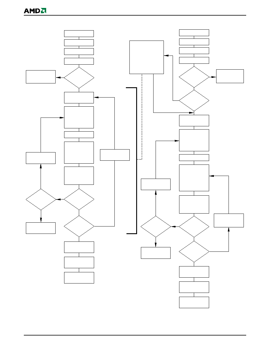
Figure 1. Temporary Sector Group
Unprotect Operation
START
Perform Erase or
Program Operations
RESET# = V
IH
Temporary Sector
Group Unprotect
Completed (Note 2)
RESET# = V
ID
(Note 1)
Notes:
1. All protected sector groups unprotected.
2. All previously protected sector groups are protected
once again.
22
Am29LV652D
October 29, 2004
P R E L I M I N A R Y
Figure 2. In-System Sector Group Protect/Unprotect Algorithms
Sector Group Protect:
Write 60h to sector
group address with
A6 = 0, A1 = 1,
A0 = 0
Set up sector
group address
Wait 150 µs
Verify Sector Group
Protect: Write 40h
to sector group
address twith A6 = 0,
A1 = 1, A0 = 0
Read from
sector group address
with A6 = 0,
A1 = 1, A0 = 0
START
PLSCNT = 1
RESET# = V
ID
Wait 1
µs
First Write
Cycle = 60h?
Data = 01h?
Remove V
ID
from RESET#
Write reset
command
Sector Group
Protect complete
Yes
Yes
No
PLSCNT
= 25?
Yes
Device failed
Increment
PLSCNT
Temporary Sector
Group Unprotect
Mode
No
Sector Group
Unprotect:
Write 60h to sector
group address with
A6 = 1, A1 = 1,
A0 = 0
Set up first sector
group address
Wait 15 ms
Verify Sector Group
Unprotect: Write
40h to sector group
address with
A6 = 1, A1 = 1,
A0 = 0
Read from
sector group
address with A6 = 1,
A1 = 1, A0 = 0
START
PLSCNT = 1
RESET# = V
ID
Wait 1
µs
Data = 00h?
Last sector
group
verified?
Remove V
ID
from RESET#
Write reset
command
Sector Group
Unprotect complete
Yes
No
PLSCNT
= 1000?
Yes
Device failed
Increment
PLSCNT
Temporary Sector
Group Unprotect
Mode
No
All sector
groups
protected?
Yes
Protect all sector
groups: The indicated
portion of the sector
group protect algorithm
must be performed for all
unprotected sector
groups prior to issuing
the first sector group
unprotect address
Set up
next sector group
address
No
Yes
No
Yes
No
No
Yes
No
Sector Group
Protect
Algorithm
Sector Group
Unprotect
Algorithm
First Write
Cycle = 60h?
Protect
another
sector group?
Reset
PLSCNT = 1
October 29, 2004
Am29LV652D
23
P R E L I M I N A R Y
Hardware Data Protection
The command sequence requirement of unlock cycles
for programming or erasing provides data protection
against inadvertent writes (refer to
Table 10, on
page 30
for command definitions). In addition, the fol-
lowing hardware data protection measures prevent ac-
cidental erasure or programming, which might
otherwise be caused by spurious system level signals
during V
CC
power-up and power-down transitions, or
from system noise.
Low V
CC
Write Inhibit
When V
CC
is less than V
LKO
, the device does not ac-
cept any write cycles. This protects data during V
CC
power-up and power-down. The command register
and all internal program/erase circuits are disabled,
and the device resets to the read mode. Subsequent
writes are ignored until V
CC
is greater than V
LKO
. The
system must provide the proper signals to the control
inputs to prevent unintentional writes when V
CC
is
greater than V
LKO
.
Write Pulse "Glitch" Protection
Noise pulses of less than 5 ns (typical) on OE#, CE#,
CE2#, or WE# do not initiate a write cycle.
Logical Inhibit
Write cycles are inhibited by holding any one of OE# =
V
IL
, CE# = V
IH
, CE2# = V
IH
or WE# = V
IH
. To initiate a
write cycle, CE# (or CE2#), and WE# must be a logical
zero while OE# is a logical one.
Power-Up Write Inhibit
If WE# = CE# = CE2# = V
IL
and OE# = V
IH
during
power up, the device does not accept commands on
the rising edge of WE#. The internal state machine is
automatically reset to the read mode on power-up.
COMMON FLASH MEMORY INTERFACE (CFI)
The Common Flash Interface (CFI) specification out-
lines device and host system software interrogation
handshake, which allows specific vendor-specified
software algorithms to be used for entire families of
devices. Software support can then be device-inde-
pendent, JEDEC ID-independent, and forward- and
backward-compatible for the specified flash device
families. Flash vendors can standardize their existing
interfaces for long-term compatibility.
The Am29LV652 is a two die solution which appears
as two 64 Mbit Am29LV065 devices in the system.
This allows the same CFI information to be used be-
cause the system "sees" two 64 Mbit devices, not a
single 128 Mbit device.
This device enters the CFI Query mode when the sys-
tem writes the CFI Query command, 98h, any time the
device is ready to read array data (addresses are don't
care). The system can read CFI information at the ad-
dresses given in
Table 6, on page 23
to
Table 9, on
page 25
. To terminate reading CFI data, the system
must write the reset command.
The system can also write the CFI query command
when the device is in the autoselect mode. The device
enters the CFI query mode, and the system can read
CFI data at the addresses given in
Table 6, on
page 23
to
Table 9, on page 25
. The system must
write the reset command to return the device to the
autoselect mode.
For further information, please refer to the CFI Specifi-
cation and CFI Publication 100, available via the
World Wide Web at http://www.amd.com/prod-
ucts/nvd/overview/cfi.html. Alternatively, contact an
AMD representative for copies of these documents.
Table 6. CFI Query Identification String
Addresses (x8)
Data
Description
10h
11h
12h
51h
52h
59h
Query Unique ASCII string "QRY"
13h
14h
02h
00h
Primary OEM Command Set
15h
16h
40h
00h
Address for Primary Extended Table
17h
18h
00h
00h
Alternate OEM Command Set (00h = none exists)
19h
1Ah
00h
00h
Address for Alternate OEM Extended Table (00h = none exists)
24
Am29LV652D
October 29, 2004
P R E L I M I N A R Y
Table 7. System Interface String
Table 8. Device Geometry Definition
Addresses (x8)
Data
Description
1Bh
27h
V
CC
Min. (write/erase)
D7≠D4: volt, D3≠D0: 100 millivolt
1Ch
36h
V
CC
Max. (write/erase)
D7≠D4: volt, D3≠D0: 100 millivolt
1Dh
00h
V
PP
Min. voltage (00h = no V
PP
input present)
1Eh
00h
V
PP
Max. voltage (00h = no V
PP
input present)
1Fh
04h
Typical timeout per single byte write 2
N
µs
20h
00h
Typical timeout for Min. size buffer write 2
N
µ
s (00h = not supported)
21h
0Ah
Typical timeout per individual block erase 2
N
ms
22h
00h
Typical timeout for full chip erase 2
N
ms (00h = not supported)
23h
05h
Max. timeout for byte write 2
N
times typical
24h
00h
Max. timeout for buffer write 2
N
times typical
25h
04h
Max. timeout per individual block erase 2
N
times typical
26h
00h
Max. timeout for full chip erase 2
N
times typical (00h = not supported)
Addresses (x8)
Data
Description
27h
17h
Device Size = 2
N
byte
28h
29h
00h
00h
Flash Device Interface description (refer to CFI publication 100)
2Ah
2Bh
00h
00h
Max. number of bytes in multi-byte write = 2
N
(00h = not supported)
2Ch
01h
Number of Erase Block Regions within device
2Dh
2Eh
2Fh
30h
7Fh
00h
00h
01h
Erase Block Region 1 Information
(refer to the CFI specification or CFI publication 100)
31h
32h
33h
34h
00h
00h
00h
00h
Erase Block Region 2 Information (refer to CFI publication 100)
35h
36h
37h
38h
00h
00h
00h
00h
Erase Block Region 3 Information (refer to CFI publication 100)
39h
3Ah
3Bh
3Ch
00h
00h
00h
00h
Erase Block Region 4 Information (refer to CFI publication 100)
October 29, 2004
Am29LV652D
25
P R E L I M I N A R Y
Table 9. Primary Vendor-Specific Extended Query
COMMAND DEFINITIONS
Writing specific address and data commands or se-
quences into the command register initiates device op-
erations.
Table 10, on page 30
defines the valid
register command sequences. Writing incorrect ad-
dress and data values or writing them in the im-
proper sequence resets the device to reading array
data.
All addresses are latched on the falling edge of WE#
or CE# (or CE2#), whichever happens later. All data is
latched on the rising edge of WE# or CE# (or CE2#),
whichever happens first. Refer to
"AC Characteristics"
on page 39
for timing diagrams.
Reading Array Data
The device is automatically set to reading array data
after device power-up. No commands are required to
retrieve data. The device is ready to read array data
after completing an Embedded Program or Embedded
Erase algorithm.
After the device accepts an Erase Suspend command,
the device enters the erase-suspend-read mode, after
w h i c h t h e s y s t e m c a n r e a d d a ta f r o m a n y
non-erase-suspended sector. After completing a pro-
gramming operation in the Erase Suspend mode, the
system may once again read array data with the same
exception. See
"Erase Suspend/Erase Resume Com-
mands" on page 28
for more information.
The system must issue the reset command to return
the device to the read (or erase-suspend-read) mode
if DQ5 goes high during an active program or erase
operation, or if the device is in the autoselect mode.
Addresses (x8)
Data
Description
40h
41h
42h
50h
52h
49h
Query-unique ASCII string "PRI"
43h
31h
Major version number, ASCII
44h
31h
Minor version number, ASCII
45h
01h
Address Sensitive Unlock (Bits 1-0)
0 = Required, 1 = Not Required
Silicon Revision Number (Bits 7-2)
46h
02h
Erase Suspend
0 = Not Supported, 1 = To Read Only, 2 = To Read & Write
47h
04h
Sector Protect
0 = Not Supported, X = Number of sectors in per group
48h
01h
Sector Temporary Unprotect
00 = Not Supported, 01 = Supported
49h
04h
Sector Protect/Unprotect scheme
04 = 29LV800 mode
4Ah
00h
Simultaneous Operation
00 = Not Supported, X = Number of Sectors in Bank
4Bh
000h
Burst Mode Type
00 = Not Supported, 01 = Supported
4Ch
00h
Page Mode Type
00 = Not Supported
4Dh
B5h
ACC (Acceleration) Supply Minimum
00h = Not Supported, D7-D4: Volt, D3-D0: 100 mV
4Eh
C5h
ACC (Acceleration) Supply Maximum
00h = Not Supported, D7-D4: Volt, D3-D0: 100 mV
4Fh
00h
Top/Bottom Boot Sector Flag
02h = Bottom Boot Device, 03h = Top Boot Device

26
Am29LV652D
October 29, 2004
P R E L I M I N A R Y
See the next section,
"Reset Command"
, for more in-
formation.
See also
"VersatileIO
TM (V
IO
) Control" on page 9
for
more information. The Read-Only Operations table
provides the read parameters, and
Figure 13, on page
39
shows the timing diagram.
Reset Command
Writing the reset command resets the device to the
read or erase-suspend-read mode. Address bits are
don't cares for this command.
The reset command may be written between the se-
quence cycles in an erase command sequence before
erasing begins. This resets the device to the read
mode. Once erasure begins, however, the device ig-
nores reset commands until the operation is complete.
The reset command may be written between the
sequence cycles in a program command sequence
before programming begins. This resets the device to
the read mode. If the program command sequence is
written while the device is in the Erase Suspend mode,
writing the reset command returns the device to the
erase-suspend-read mode. Once programming be-
gins, however, the device ignores reset commands
until the operation is complete.
The reset command may be written between the se-
quence cycles in an autoselect command sequence.
Once in the autoselect mode, the reset command
must be written to return to the read mode. If the de-
vice entered the autoselect mode while in the Erase
Suspend mode, writing the reset command returns the
device to the erase-suspend-read mode.
If DQ5 goes high during a program or erase operation,
writing the reset command returns the device to the
read mode (or erase-suspend-read mode if the device
was in Erase Suspend).
Autoselect Command Sequence
The autoselect command sequence allows the host
system to access the manufacturer and device codes,
and determine whether or not a sector is protected.
Table 10, on page 30
shows the address and data re-
quirements. This method is an alternative to that
shown in
Table 4, on page 19
, which is intended for
PROM programmers and requires V
ID
on address A9.
The autoselect command sequence may be written to
a n a d d r e s s t h a t i s e i t h e r i n t h e r e a d o r
erase-suspend-read mode. The autoselect command
may not be written while the device is actively pro-
gramming or erasing.
The autoselect command sequence is initiated by first
writing two unlock cycles. This is followed by a third
write cycle that contains the autoselect command. The
device then enters the autoselect mode. The system
may read at any address any number of times without
initiating another autoselect command sequence:
A read cycle at address XX00h returns the manu-
facturer code.
A read cycle at address XX01h returns the device
code.
A read cycle to an address containing a sector
group address (SA), and the address 02h on A7≠A0
returns 01h if the sector group is protected, or 00h
if it is unprotected. (Refer to
Table 5, on page 20
for
valid sector addresses).
The system must write the reset command to return to
the read mode (or erase-suspend-read mode if the de-
vice was previously in Erase Suspend).
Byte Program Command Sequence
Programming is a four-bus-cycle operation. The pro-
gram command sequence is initiated by writing two
unlock write cycles, followed by the program set-up
command. The program address and data are written
next, which in turn initiate the Embedded Program al-
gorithm. The system is not required to provide further
controls or timings. The device automatically provides
internally generated program pulses and verifies the
programmed cell margin.
Table 10, on page 30
shows
the address and data requirements for the byte pro-
gram command sequence.
When the Embedded Program algorithm is complete,
the device then returns to the read mode and ad-
dresses are no longer latched. The system can deter-
mine the status of the program operation by using
DQ7, DQ6, or RY/BY#. Refer to the
"Write Operation
Status" on page 31
section for information on these
status bits.
Any commands written to the device during the Em-
bedded Program Algorithm are ignored. Note that a
hardware reset immediately terminates the program
operation. The program command sequence should
be reinitiated once the device returns to the read
mode, to ensure data integrity.
Programming is allowed in any sequence and across
sector boundaries. A bit cannot be programmed
from "0" back to a "1." Attempting to do so may
cause the device to set DQ5 = 1, or cause the DQ7
and DQ6 status bits to indicate the operation was suc-
cessful. However, a succeeding read shows that the
data is still "0." Only erase operations can convert a
"0" to a "1."
Unlock Bypass Command Sequence
The unlock bypass feature allows the system to pro-
gram bytes to the device faster than using the stan-
dard program command sequence. The unlock
bypass command sequence is initiated by first writing
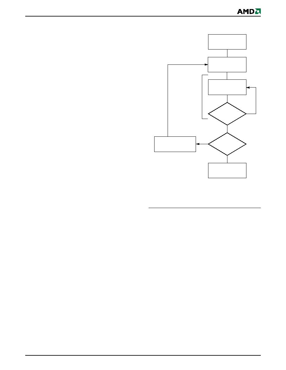
October 29, 2004
Am29LV652D
27
P R E L I M I N A R Y
two unlock cycles. This is followed by a third write
cycle containing the unlock bypass command, 20h.
The device then enters the unlock bypass mode. A
two-cycle unlock bypass program command sequence
is all that is required to program in this mode. The first
cycle in this sequence contains the unlock bypass pro-
gram command, A0h; the second cycle contains the
program address and data. Additional data is pro-
grammed in the same manner. This mode dispenses
with the initial two unlock cycles required in the stan-
dard program command sequence, resulting in faster
total programming time.
Table 10, on page 30
shows
the requirements for the command sequence.
During the unlock bypass mode, only the Unlock By-
pass Program and Unlock Bypass Reset commands
are valid. To exit the unlock bypass mode, the system
must issue the two-cycle unlock bypass reset com-
mand sequence. The first cycle must contain the data
90h. The second cycle must contain the data 00h. The
device then returns to the read mode.
The device offers accelerated program operations
through ACC. When the system asserts V
HH
on ACC,
the device automatically enters the Unlock Bypass
mode. The system may then write the two-cycle Un-
lock Bypass program command sequence. The device
uses the higher voltage on ACC to accelerate the op-
eration. Note that ACC must not be at V
HH
for opera-
tions other than accelerated programming, or device
damage may result.
Figure 3, on page 27
illustrates the algorithm for the
program operation. Refer to the
"Erase and Program
Operations" on page 41
table in the AC Characteris-
tics section for parameters, and
Figure 15, on page 42
for timing diagrams.
Figure 3. Program Operation
Chip Erase Command Sequence
Chip erase is a six bus cycle operation. The chip erase
command sequence is initiated by writing two unlock
cycles, followed by a set-up command. Two additional
unlock write cycles are then followed by the chip erase
command, which in turn invokes the Embedded Erase
algorithm. The device does not require the system to
preprogram prior to erase. The Embedded Erase algo-
rithm automatically preprograms and verifies the entire
memory for an all zero data pattern prior to electrical
erase. The system is not required to provide any con-
trols or timings during these operations.
Table 10, on
page 30
shows the address and data requirements for
the chip erase command sequence.
START
Write Program
Command Sequence
Data Poll
from System
Verify Data?
No
Yes
Last Address?
No
Yes
Programming
Completed
Increment Address
Embedded
Program
algorithm
in progress
Note: See
Table 10, on page 30
for program command
sequence.

28
Am29LV652D
October 29, 2004
P R E L I M I N A R Y
When the Embedded Erase algorithm is complete, the
device returns to the read mode and addresses are no
longer latched. The system can determine the status
of the erase operation by using DQ7, DQ6, DQ2, or
RY/BY#. Refer to
"Write Operation Status" on page 31
for information on these status bits.
Any commands written during the chip erase operation
are ignored. However, note that a hardware reset im-
mediately terminates the erase operation. If that oc-
curs, the chip erase command sequence should be
reinitiated once the device returns to reading array
data, to ensure data integrity.
Figure 4, on page 29
illustrates the algorithm for the
erase operation. Refer to the
"Erase and Program Op-
erations" on page 41
tables in the AC Characteristics
section for parameters, and
Figure 17, on page 43
section for timing diagrams.
Sector Erase Command Sequence
Sector erase is a six bus cycle operation. The sector
erase command sequence is initiated by writing two
unlock cycles, followed by a set-up command. Two ad-
ditional unlock cycles are written, and are then fol-
lowed by the address of the sector to be erased, and
the sector erase command.
Table 10, on page 30
shows the address and data requirements for the sec-
tor erase command sequence.
The device does not require the system to preprogram
prior to erase. The Embedded Erase algorithm auto-
matically programs and verifies the entire memory for
an all zero data pattern prior to electrical erase. The
system is not required to provide any controls or tim-
ings during these operations.
After the command sequence is written, a sector erase
time-out of 50 µs occurs. During the time-out period,
additional sector addresses and sector erase com-
mands may be written. Loading the sector erase buffer
may be done in any sequence, and the number of sec-
tors may be from one sector to all sectors. The time
between these additional cycles must be less than 50
µs, otherwise erasure may begin. Any sector erase
address and command following the exceeded
time-out may or may not be accepted. It is recom-
mended that processor interrupts be disabled during
this time to ensure all commands are accepted. The
interrupts can be re-enabled after the last Sector
Erase command is written. Any command other than
Sector Erase or Erase Suspend during the
time-out period resets the device to the read
mode. The system must rewrite the command se-
quence and any additional addresses and commands.
The system can monitor DQ3 to determine if the sec-
tor erase timer has timed out (See
"DQ3: Sector Erase
Timer" on page 33
.). The time-out begins from the ris-
ing edge of the final WE# pulse in the command
sequence.
When the Embedded Erase algorithm is complete, the
device returns to reading array data and addresses
are no longer latched. Note that while the Embedded
Erase operation is in progress, the system can read
data from the non-erasing sector. The system can de-
termine the status of the erase operation by reading
DQ7, DQ6, DQ2, or RY/BY# in the erasing sector.
Refer to
"Write Operation Status" on page 31
for infor-
mation on these status bits.
Once the sector erase operation begins, only the
Erase Suspend command is valid. All other com-
mands are ignored. However, note that a hardware
reset immediately terminates the erase operation. If
that occurs, the sector erase command sequence
should be reinitiated once the device returns to read-
ing array data, to ensure data integrity.
Figure 4, on page 29
illustrates the algorithm for the
erase operation. Refer to the
"Erase and Program Op-
erations" on page 41
tables in the AC Characteristics
section for parameters, and
Figure 17, on page 43
section for timing diagrams.
Erase Suspend/Erase Resume
Commands
The Erase Suspend command, B0h, allows the sys-
tem to interrupt a sector erase operation and then read
data from, or program data to, any sector not selected
for erasure. This command is valid only during the
sector erase operation, including the 50 µs time-out
period during the sector erase command sequence.
The Erase Suspend command is ignored if written dur-
ing the chip erase operation or Embedded Program
algorithm.
When the Erase Suspend command is written during
the sector erase operation, the device requires a max-
imum of 20 µs to suspend the erase operation. How-
ever, when the Erase Suspend command is written
during the sector erase time-out, the device immedi-
ately terminates the time-out period and suspends the
erase operation.
After the erase operation is suspended, the device en-
ters the erase-suspend-read mode. The system can
read data from or program data to any sector not se-
lected for erasure. (The device "erase suspends" all
sectors selected for erasure.) Reading at any address
within erase-suspended sectors produces status infor-
mation on DQ7≠DQ0. The system can use DQ7, or
DQ6 and DQ2 together, to determine if a sector is ac-
tively erasing or is erase-suspended. Refer to
"Write
Operation Status" on page 31
for information on these
status bits.
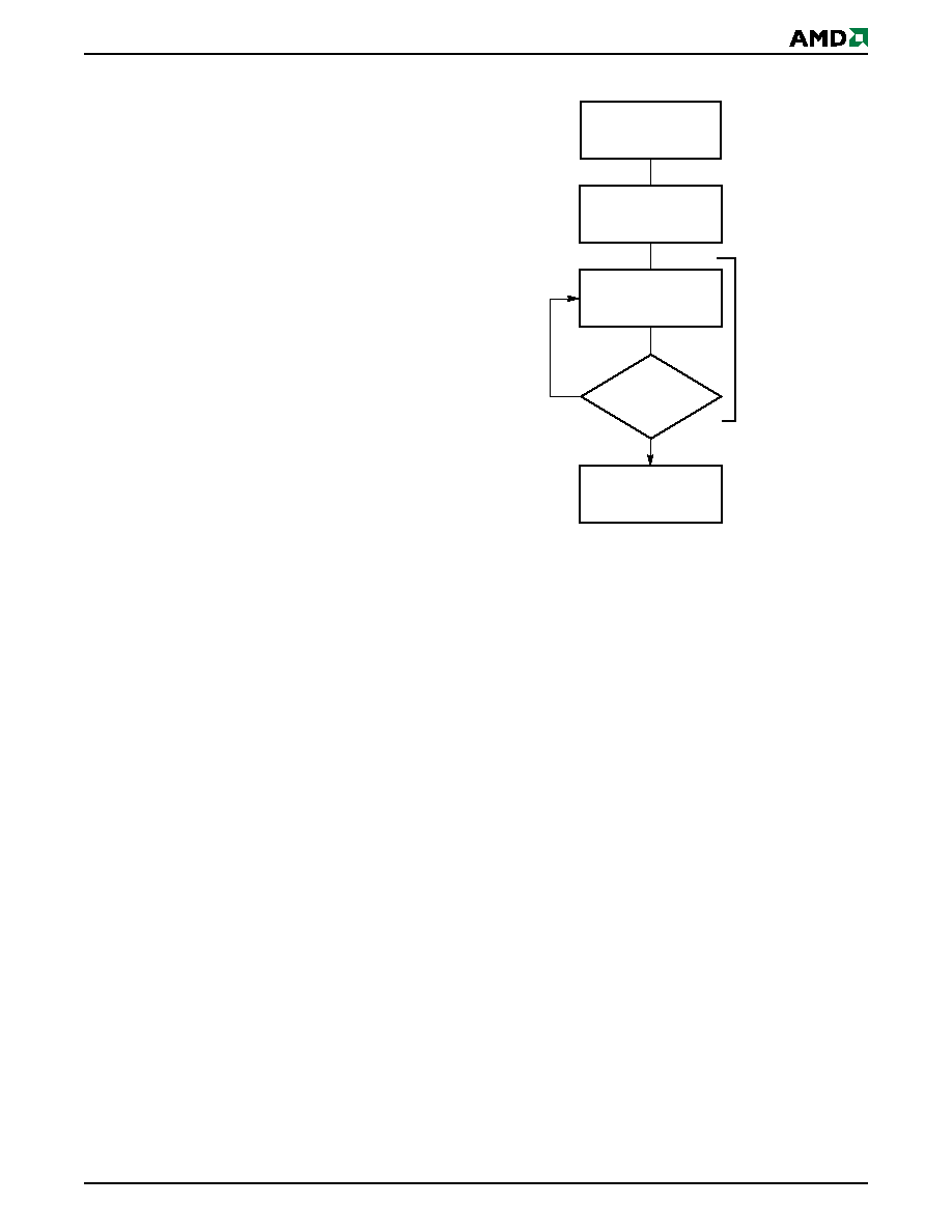
October 29, 2004
Am29LV652D
29
P R E L I M I N A R Y
After an erase-suspended program operation is com-
plete, the device returns to the erase-suspend-read
mode. The system can determine the status of the
program operation using the DQ7 or DQ6 status bits,
just as in the standard byte program operation.
Refer to
"Write Operation Status" on page 31
for more
information.
In the erase-suspend-read mode, the system can also
issue the autoselect command sequence. Refer to the
"Autoselect Mode" on page 19
and
"Autoselect Com-
mand Sequence" on page 26
sections for details.
To resume the sector erase operation, the system
must write the Erase Resume command. The address
of the erase-suspended sector is required when writ-
ing this command. Further writes of the Resume com-
mand are ignored. Another Erase Suspend command
can be written after the chip resumes erasing.
Figure 4. Erase Operation
START
Write Erase
Command Sequence
(Notes 1, 2)
Data Poll to Erasing
Bank from System
Data = FFh?
No
Yes
Erasure Completed
Embedded
Erase
algorithm
in progress
Notes:
1. See
Table 10, on page 30
for erase command
sequence.
2. See the section on DQ3 for information on the sector
erase timer.
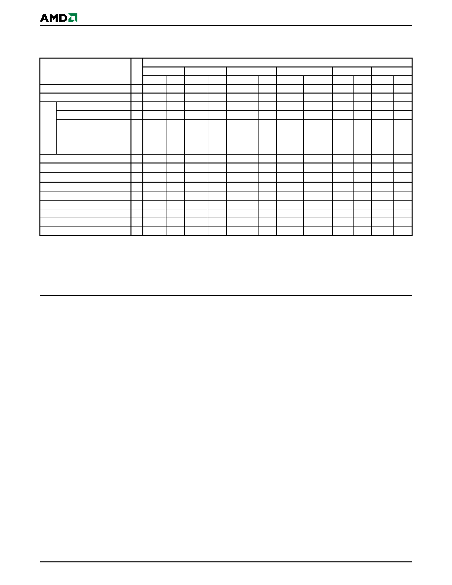
30
Am29LV652D
October 29, 2004
P R E L I M I N A R Y
Command Definitions
Table 10. Am29LV652D Command Definitions
Legend:
X = Don't care
RA = Address of the memory location to be read.
RD = Data read from location RA during read operation.
PA = Address of the memory location to be programmed. Addresses
latch on the falling edge of the WE# or CE# (or CE2#) pulse, whichever
happens later.
PD = Data to be programmed at location PA. Data latches on the rising
edge of WE# or CE# (or CE2#) pulse, whichever happens first.
SA = Address of the sector to be verified (in autoselect mode) or
erased. Address bits A22≠A16 uniquely select any sector.
Notes:
1. See
Table 1, on page 9
for description of bus operations.
2. All values are in hexadecimal.
3. Except for the read cycle and the fourth cycle of the autoselect
command sequence, all bus cycles are write cycles.
4. Unless otherwise noted, address bits A22≠A12 are don't cares.
5. No unlock or command cycles required when device is in read
mode.
6. The Reset command is required to return to the read mode (or to
the erase-suspend-read mode if previously in Erase Suspend)
when the device is in the autoselect mode, or if DQ5 goes high
(while the device is providing status information).
7. The fourth cycle of the autoselect command sequence is a read
cycle. See the Autoselect Command Sequence section for more
information.
8. The data is 00h for an unprotected sector group and 01h for a
protected sector group.
9. The Unlock Bypass command is required prior to the Unlock
Bypass Program command.
10. The Unlock Bypass Reset command is required to return to the
read mode when the device is in the unlock bypass mode.
11. The system may read and program in non-erasing sectors, or
enter the autoselect mode, when in the Erase Suspend mode.
The Erase Suspend command is valid only during a sector erase
operation.
12. The Erase Resume command is valid only during the Erase
Suspend mode.
13. Command is valid when device is ready to read array data or when
device is in autoselect mode.
Command
Sequence
(Note 1)
Cycle
s
Bus Cycles (Notes 2≠4)
First
Second Third
Fourth Fifth Sixth
Addr
Data
Addr
Data
Addr
Data
Addr
Data
Addr
Data
Addr
Data
Read (Note 5)
1
RA
RD
Reset (Note 6)
1
XXX
F0
Auto
s
e
l
e
c
t
(
N
ote 7)
Manufacturer ID
4
XXX
AA
XXX
55
XXX
90
X00
01
Device ID
4
XXX
AA
XXX
55
XXX
90
X01
93
Sector Group Protect Verify
(Note 8)
4
XXX
AA
XXX
55
XXX
90
(SA)X02
00/01
Program
4
XXX
AA
XXX
55
XXX
A0
PA
PD
Unlock Bypass
3
XXX
AA
XXX
55
XXX
20
Unlock Bypass Program (Note 9)
2
XXX
A0
PA
PD
Unlock Bypass Reset (Note 10)
2
XXX
90
XXX
00
Chip Erase
6
XXX
AA
XXX
55
XXX
80
XXX
AA
XXX
55
XXX
10
Sector Erase
6
XXX
AA
XXX
55
XXX
80
XXX
AA
XXX
55
SA
30
Erase Suspend (Note 11)
1
BA
B0
Erase Resume (Note 12)
1
BA
30
CFI Query (Note 13)
1
XX
98
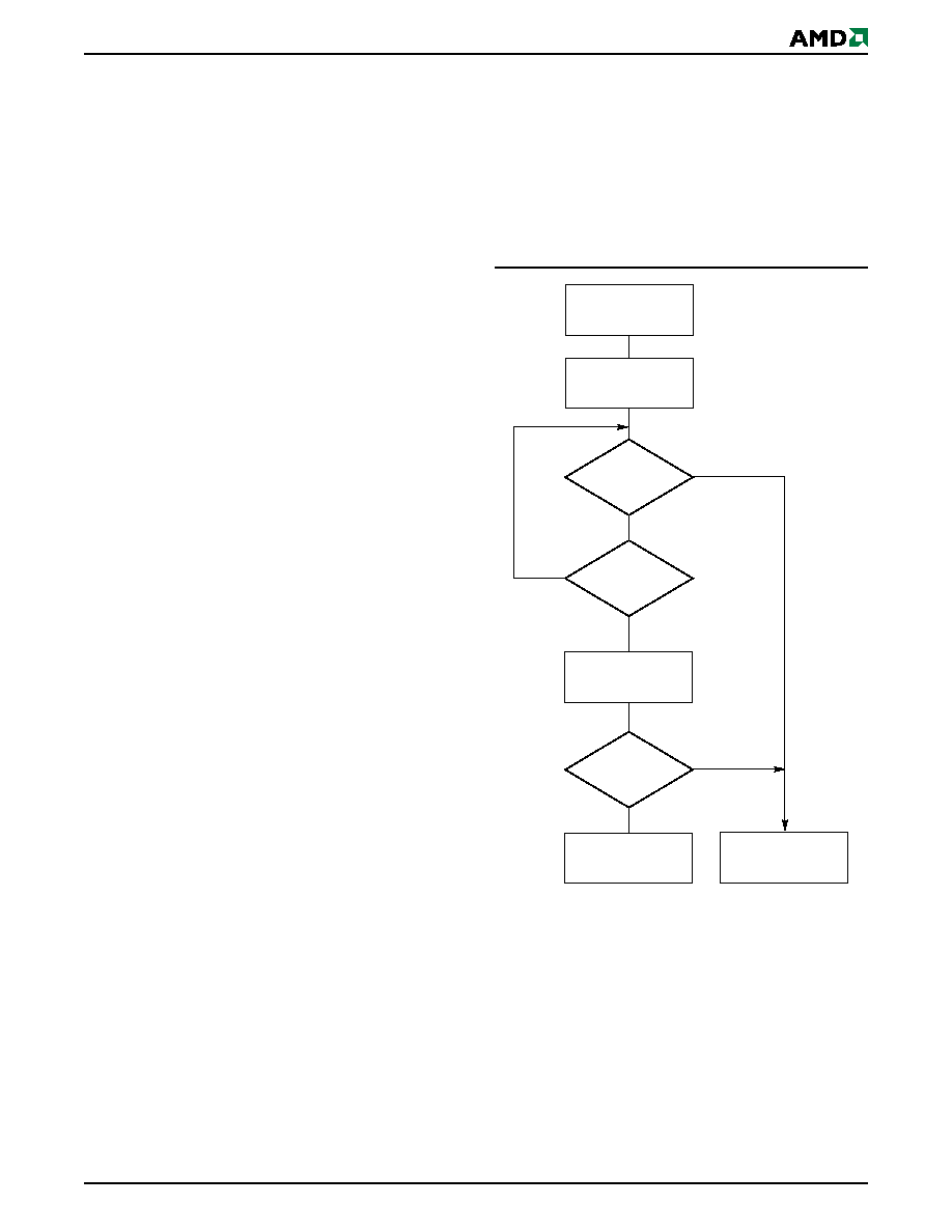
October 29, 2004
Am29LV652D
31
P R E L I M I N A R Y
WRITE OPERATION STATUS
The device provides several bits to determine the status of a
program or erase operation: DQ2, DQ3, DQ5, DQ6, and
DQ7.
Table 11, on page 34
and the following subsections
describe the function of these bits. DQ7 and DQ6 each offer
a method for determining whether a program or erase oper-
ation is complete or in progress. The device also provides a
hardware-based output signal, RY/BY#, to determine
whether an Embedded Program or Erase operation is in
progress or is completed.
DQ7: Data# Polling
The Data# Polling bit, DQ7, indicates to the host system
whether an Embedded Program or Erase algorithm is in
progress or completed, or whether the device is in Erase
Suspend. Data# Polling is valid after the rising edge of the
final WE# pulse in the command sequence.
During the Embedded Program algorithm, the device out-
puts on DQ7 the complement of the datum programmed to
DQ7. This DQ7 status also applies to programming during
Erase Suspend. When the Embedded Program algorithm is
complete, the device outputs the datum programmed to
DQ7. The system must provide the program address to
read valid status information on DQ7. If a program address
falls within a protected sector, Data# Polling on DQ7 is ac-
tive for approximately 1 µs, then the device returns to the
read mode.
During the Embedded Erase algorithm, Data# Polling
produces a "0" on DQ7. When the Embedded Erase
algorithm is complete, or if the device enters the Erase
Suspend mode, Data# Polling produces a "1" on DQ7.
The system must provide an address within any of the
sectors selected for erasure to read valid status infor-
mation on DQ7.
After an erase command sequence is written, if all
sectors selected for erasing are protected, Data# Poll-
ing on DQ7 is active for approximately 100 µs, then
the device returns to the read mode. If not all selected
sectors are protected, the Embedded Erase algorithm
erases the unprotected sectors, and ignores the se-
lected sectors that are protected. However, if the sys-
tem reads DQ7 at an address within a protected
sector, the status may not be valid.
Just prior to the completion of an Embedded Program
or Erase operation, DQ7 may change asynchronously
with DQ0≠DQ6 while Output Enable (OE#) is asserted
low. That is, the device may change from providing
status information to valid data on DQ7. Depending on
when the system samples the DQ7 output, it may read
the status or valid data. Even if the device completes
the program or erase operation and DQ7 contains
valid data, the data outputs on DQ0≠DQ6 may be still
invalid. Valid data on DQ0≠DQ7 appears on succes-
sive read cycles.
"Write Operation Status" on page 34
shows the out-
puts for Data# Polling on DQ7.
Figure 5
shows the
Data# Polling algorithm.
Figure 18, on page 44
in the
AC Characteristics section shows the Data# Polling
timing diagram.
Figure 5. Data# Polling Algorithm
DQ7 = Data?
Yes
No
No
DQ5 = 1?
No
Yes
Yes
FAIL
PASS
Read DQ7≠DQ0
Addr = VA
Read DQ7≠DQ0
Addr = VA
DQ7 = Data?
START
Notes:
1. VA = Valid address for programming. During a sector
erase operation, a valid address is any sector address
within the sector being erased. During chip erase, a
valid address is any non-protected sector address.
2. DQ7 should be rechecked even if DQ5 = "1" because
DQ7 may change simultaneously with DQ5.

32
Am29LV652D
October 29, 2004
P R E L I M I N A R Y
RY/BY#: Ready/Busy#
The RY/BY# is a dedicated, open-drain output which
indicates whether an Embedded Algorithm is in
progress or complete. The RY/BY# status is valid after
the rising edge of the final WE# pulse in the command
sequence. Since RY/BY# is an open-drain output, sev-
eral RY/BY#s can be tied together in parallel with a
pull-up resistor to V
CC
.
If the output is low (Busy), the device is actively eras-
ing or programming. (This includes programming in
the Erase Suspend mode.) If the output is high
(Ready), the device is in the read mode, the standby
mode, or the device is in the erase-suspend-read
mode.
Table 11, on page 34
shows the outputs for RY/BY#.
DQ6: Toggle Bit I
Toggle Bit I on DQ6 indicates whether an Embedded
Program or Erase algorithm is in progress or com-
plete, or whether the device has entered the Erase
Suspend mode. Toggle Bit I may be read at any ad-
dress, and is valid after the rising edge of the final
WE# pulse in the command sequence (prior to the
program or erase operation), and during the sector
erase time-out.
During an Embedded Program or Erase algorithm op-
eration, successive read cycles to any address cause
DQ6 to toggle. The system may use either OE# or
CE# (or CE2#) to control the read cycles. When the
operation is complete, DQ6 stops toggling.
After an erase command sequence is written, if all sectors
selected for erasing are protected, DQ6 toggles for approxi-
mately 100 µs, then returns to reading array data. If not all
selected sectors are protected, the Embedded Erase algo-
rithm erases the unprotected sectors, and ignores the se-
lected sectors that are protected.
The system can use DQ6 and DQ2 together to determine
whether a sector is actively erasing or is erase-suspended.
When the device is actively erasing (that is, the Embedded
Erase algorithm is in progress), DQ6 toggles. When the de-
vice enters the Erase Suspend mode, DQ6 stops toggling.
However, the system must also use DQ2 to determine
which sectors are erasing or erase-suspended. Alterna-
tively, the system can use DQ7 (see the subsection on
"DQ7: Data# Polling" on page 31
).
If a program address falls within a protected sector,
DQ6 toggles for approximately 1
µs after the program
command sequence is written, then returns to reading
array data.
DQ6 also toggles during the erase-suspend-program
mode, and stops toggling once the Embedded Pro-
gram algorithm is complete.
Table 11, on page 34
shows the outputs for Toggle Bit
I on DQ6.
Figure 6
shows the toggle bit algorithm.
Fig-
ure 19, on page 45
in the "AC Characteristics" section
shows the toggle bit timing diagrams.
Figure 20, on
page 45
shows the differences between DQ2 and DQ6
in graphical form. See also the subsection
"DQ2: Tog-
gle Bit II" on page 33
.
Figure 6. Toggle Bit Algorithm
START
No
Yes
Yes
DQ5 = 1?
No
Yes
Toggle Bit
= Toggle?
No
Program/Erase
Operation Not
Complete, Write
Reset Command
Program/Erase
Operation Complete
Read DQ7≠DQ0
Toggle Bit
= Toggle?
Read DQ7≠DQ0
Twice
Read DQ7≠DQ0
Note: The system should recheck the toggle bit even if
DQ5 = "1" because the toggle bit may stop toggling as DQ5
changes to "1." See the subsections on DQ6 and DQ2 for
more information.

October 29, 2004
Am29LV652D
33
P R E L I M I N A R Y
DQ2: Toggle Bit II
The "Toggle Bit II" on DQ2, when used with DQ6, indi-
cates whether a particular sector is actively erasing
(that is, the Embedded Erase algorithm is in progress),
or whether that sector is erase-suspended. Toggle Bit
II is valid after the rising edge of the final WE# pulse in
the command sequence.
DQ2 toggles when the system reads at addresses
within those sectors that have been selected for era-
sure. (The system may use either OE# or CE# or
CE2# to control the read cycles.) But DQ2 cannot dis-
tinguish whether the sector is actively erasing or is
erase-suspended. DQ6, by comparison, indicates
whether the device is actively erasing, or is in Erase
Suspend, but cannot distinguish which sectors are se-
lected for erasure. Thus, both status bits are required
for sector and mode information. Refer to
Table 11, on
page 34
to compare outputs for DQ2 and DQ6.
Figure 6, on page 32
shows the toggle bit algorithm in
flowchart form, and the section "DQ2: Toggle Bit II" ex-
plains the algorithm. See also the DQ6: Toggle Bit I
subsection.
Figure 19, on page 45
shows the toggle bit
timing diagram.
Figure 20, on page 45
shows the dif-
ferences between DQ2 and DQ6 in graphical form.
Reading Toggle Bits DQ6/DQ2
Refer to
Figure 6, on page 32
for the following discus-
sion. Whenever the system initially begins reading tog-
gle bit status, it must read DQ7≠DQ0 at least twice in a
row to determine whether a toggle bit is toggling. Typi-
cally, the system would note and store the value of the
toggle bit after the first read. After the second read, the
system would compare the new value of the toggle bit
with the first. If the toggle bit is not toggling, the device
has completed the program or erase operation. The
system can read array data on DQ7≠DQ0 on the fol-
lowing read cycle.
However, if after the initial two read cycles, the system
determines that the toggle bit is still toggling, the sys-
tem also should note whether the value of DQ5 is high
(see the section on DQ5). If it is, the system should
then determine again whether the toggle bit is tog-
gling, since the toggle bit may have stopped toggling
just as DQ5 went high. If the toggle bit is no longer
toggling, the device has successfully completed the
program or erase operation. If it is still toggling, the de-
vice did not completed the operation successfully, and
the system must write the reset command to return to
reading array data.
The remaining scenario is that the system initially de-
termines that the toggle bit is toggling and DQ5 has
not gone high. The system may continue to monitor
the toggle bit and DQ5 through successive read cy-
cles, determining the status as described in the previ-
ous paragraph. Alternatively, it may choose to perform
other system tasks. In this case, the system must start
at the beginning of the algorithm when it returns to de-
termine the status of the operation (top of
Figure 6, on
page 32
).
DQ5: Exceeded Timing Limits
DQ5 indicates whether the program or erase time ex-
ceeded a specified internal pulse count limit. Under these
conditions DQ5 produces a "1," indicating that the program
or erase cycle was not successfully completed.
The device may output a "1" on DQ5 if the system tries
to program a "1" to a location that was previously pro-
grammed to "0." Only an erase operation can
change a "0" back to a "1." Under this condition, the
device halts the operation, and when the timing limit is
exceeded, DQ5 produces a "1."
Under both these conditions, the system must write
the reset command to return to the read mode (or to
the erase-suspend-read mode if the device was previ-
ously in the erase-suspend-program mode).
DQ3: Sector Erase Timer
After writing a sector erase command sequence, the
system may read DQ3 to determine whether or not
erasure began. (The sector erase timer does not apply
to the chip erase command.) If additional sectors are
selected for erasure, the entire time-out also applies
after each additional sector erase command. When
the time-out period is complete, DQ3 switches from a
"0" to a "1." If the time between additional sector erase
commands from the system can be assumed to be
less than 50 µs, the system need not monitor DQ3.
See also
"Sector Erase Command Sequence" on
page 28
After the sector erase command is written, the system
should read the status of DQ7 (Data# Polling) or DQ6
(Toggle Bit I) to ensure that the device accepted the
command sequence, and then read DQ3. If DQ3 is
"1," the Embedded Erase algorithm has begun; all fur-
ther commands (except Erase Suspend) are ignored
until the erase operation is complete. If DQ3 is "0," the
device accepts additional sector erase commands. To
ensure the command is accepted, the system software
should check the status of DQ3 prior to and following
each subsequent sector erase command. If DQ3 is
high on the second status check, the last command
might not have been accepted.
Table 11, on page 34
shows the status of DQ3 relative
to the other status bits.

34
Am29LV652D
October 29, 2004
P R E L I M I N A R Y
Table 11. Write Operation Status
Notes:
1. DQ5 switches to `1' when an Embedded Program or Embedded Erase operation has exceeded the maximum timing limits.
Refer to the section on DQ5 for more information.
2. DQ7 and DQ2 require a valid address when reading status information. Refer to the appropriate subsection for further details.
Status
DQ7
(Note 2)
DQ6
DQ5
(Note 1)
DQ3
DQ2
(Note 2)
RY/BY#
Standard
Mode
Embedded Program Algorithm
DQ7#
Toggle
0
N/A
No toggle
0
Embedded Erase Algorithm
0
Toggle
0
1
Toggle
0
Erase
Suspend
Mode
Erase-Suspend-
Read
Erase
Suspended Sector
1
No toggle
0
N/A
Toggle
1
Non-Erase
Suspended Sector
Data
Data
Data
Data
Data
1
Erase-Suspend-Program
DQ7#
Toggle
0
N/A
N/A
0
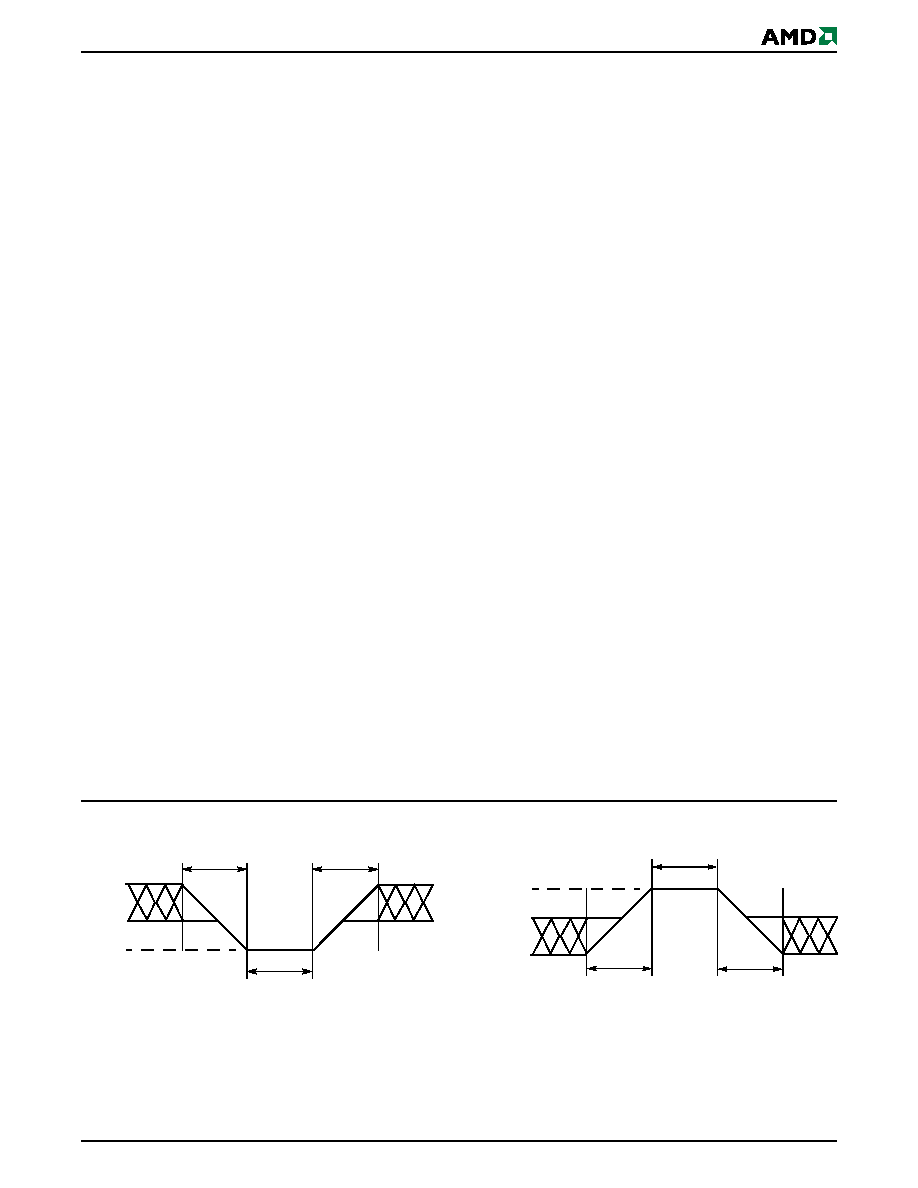
October 29, 2004
Am29LV652D
35
P R E L I M I N A R Y
ABSOLUTE MAXIMUM RATINGS
Storage Temperature
Plastic Packages . . . . . . . . . . . . . . . ≠65
∞C to +150∞C
Ambient Temperature
with Power Applied . . . . . . . . . . . . . ≠65
∞C to +125∞C
Voltage with Respect to Ground
V
CC
(Note 1) . . . . . . . . . . . . . . . . .≠0.5 V to +4.0 V
V
IO
. . . . . . . . . . . . . . . . . . . . . . . . .≠0.5 V to +5.5 V
A9, OE#, ACC, and RESET#
(Note 2) . . . . . . . . . . . . . . . . . . . .≠0.5 V to +12.5 V
All others (Note 1) . . . . . . . . . ≠0.5 V to V
CC
+0.5 V
Output Short Circuit Current (Note 3) . . . . . . 200 mA
Notes:
1. Minimum DC voltage on input or I/Os is ≠0.5 V. During
voltage transitions, input or I/Os may overshoot V
SS
to
≠2.0 V for periods of up to 20 ns. Maximum DC voltage
on input or I/Os is V
CC
+0.5 V. See
Figure 7, on page 35
.
During voltage transitions, input or I/Os may overshoot to
V
CC
+2.0 V for periods up to 20 ns. See
Figure 8, on
page 35
.
2. Minimum DC input voltage on A9, OE#, ACC, and
RESET# is ≠0.5 V. During voltage transitions, A9, OE#,
ACC, and RESET# may overshoot V
SS
to ≠2.0 V for
periods of up to 20 ns. See
Figure 7, on page 35
.
Maximum DC input voltage on A9, OE#, ACC, and
RESET# is +12.5 V which may overshoot to +14.0 V for
periods up to 20 ns.
3. No more than one output may be shorted to ground at a
time. Duration of the short circuit should not be greater
than one second.
Stresses above those listed under "Absolute Maximum
Ratings" may cause permanent damage to the device. This
is a stress rating only; functional operation of the device at
these or any other conditions above those indicated in the
operational sections of this data sheet is not implied.
Exposure of the device to absolute maximum rating
conditions for extended periods may affect device reliability.
OPERATING RANGES
Industrial (I) Devices
Ambient Temperature (T
A
) . . . . . . . . .≠40∞C to +85∞C
Extended (E) Devices
Ambient Temperature (T
A
) . . . . . . . .≠55∞C to +125∞C
Supply Voltages
V
CC
. . . . . . . . . . . . . . . . . . . . . . . . . . . . . . 3.0 V≠3.6 V
V
IO
. . . . . . . . . . . . . . . . . . . . . . . . . . . . . . . 3.0 V≠5.0 V
Operating ranges define those limits between which the
functionality of the device is guaranteed.
20 ns
20 ns
+0.8 V
≠0.5 V
20 ns
≠2.0 V
Figure 7.
Maximum Negative
Overshoot Waveform
20 ns
20 ns
V
CC
+2.0 V
V
CC
+0.5 V
20 ns
2.0 V
Figure 8.
Maximum Positive
Overshoot Waveform
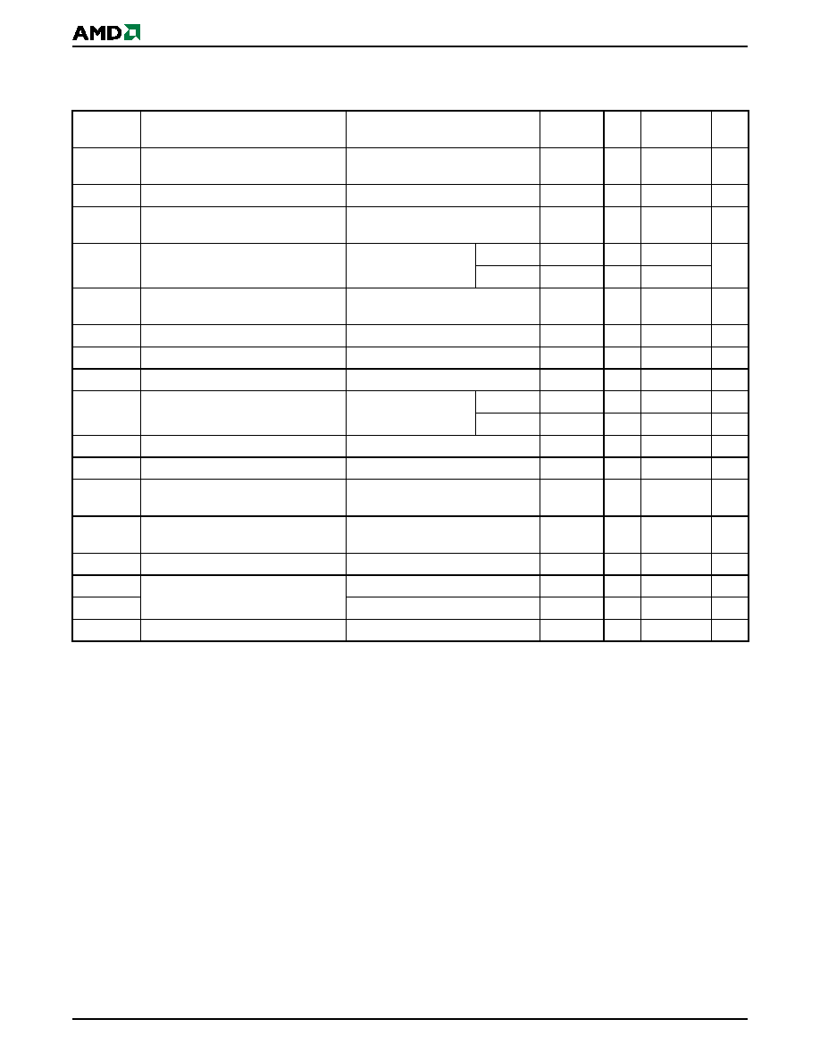
36
Am29LV652D
October 29, 2004
P R E L I M I N A R Y
DC CHARACTERISTICS (For Two Am29LV065 Devices)
CMOS Compatible
Notes:
1. The I
CC
current listed is typically less than 2 mA/MHz, with OE# at V
IH
.
2. Maximum I
CC
specifications are tested with V
CC
= V
CC
max.
3. I
CC
active while Embedded Erase or Embedded Program is in progress.
4. Assumes only one Am29LV065 die being programmed at the same time.
5. Automatic sleep mode enables the low power mode when addresses remain stable for t
ACC
+ 30 ns. Typical sleep mode current is
400 nA.
6. If V
IO
< V
CC
, maximum V
IL
for CE# (or CE2#) is 0.3 V
IO
. If V
IO
< V
CC
, minimum V
IH
for CE# (or CE2#) is 0.3 V
IO
.
7. Not 100% tested.
8. CE# can be replaced with CE2# when referring to the second device within the package.
9. Specifications in the table are for the Am29LV652 i.e. two Am29LV065 dice.
Parameter
Symbol
Parameter Description
Test Conditions
Min
Typ
Max
Unit
I
LI
Input Load Current
V
IN
= V
SS
to V
CC
,
V
CC
= V
CC
max
±1.0
µA
I
LIT
A9, ACC Input Load Current
V
CC
= V
CC max
; A9 = 12.5 V
70
µA
I
LO
Output Leakage Current
V
OUT
= V
SS
to V
CC
,
V
CC
= V
CC max
±1.0
µA
I
CC1
V
CC
Active Read Current
(Notes 1, 2)
CE# (or CE2#) = V
IL
,
OE# =
V
IH
5 MHz
9
16
mA
1 MHz
2
4
I
CC2
V
CC
Active Write Current (Notes 2, 3,
4)
CE# (or CE2#) = V
IL
, OE# =
V
IH
26
30
mA
I
CC3
V
CC
Standby Current (Note 2)
CE#, CE2#, RESET# = V
CC
± 0.3 V
0.4
10
µA
I
CC4
V
CC
Reset Current (Note 2)
RESET# = V
SS
± 0.3 V
0.4
10
µA
I
CC5
Automatic Sleep Mode (Notes 2, 5)
V
IH
= V
CC
± 0.3 V; V
IL
= V
SS
± 0.3 V
0.4
10
µA
I
ACC
ACC Accelerated Program Current
(Note 4)
CE# = V
IL
, OE# = V
IH
ACC
5
10
mA
V
CC
15
30
mA
V
IL
Input Low Voltage (Note 6)
≠0.5
0.8
V
V
IH
Input High Voltage (Note 6)
0.7 x V
CC
V
CC
+ 0.3
V
V
HH
Voltage for ACC Program
Acceleration
V
CC
= 3.0 V ± 10%
11.5
12.5
V
V
ID
Voltage for Autoselect and
Temporary Sector Unprotect
V
CC
= 3.0 V
± 10%
8.5
12.5
V
V
OL
Output Low Voltage
I
OL
= 4.0 mA, V
CC
= V
CC min
0.45
V
V
OH1
Output High Voltage (Note 7)
I
OH
= ≠2.0 mA, V
CC
= V
CC min
0.85
V
IO
V
V
OH2
I
OH
= ≠100 µA, V
CC
= V
CC min
V
IO
≠0.4
V
V
LKO
Low V
CC
Lock-Out Voltage (Note 7)
2.3
2.5
V
October 29, 2004
Am29LV652D
37
P R E L I M I N A R Y
DC CHARACTERISTICS
Zero-Power Flash
Note: Addresses are switching at 1 MHz
Figure 9. I
CC1
Current vs. Time (Showing Active and Automatic Sleep Currents)
25
20
15
10
5
0
0
500
1000
1500
2000
2500
3000
3500
4000
S
upply
Cur
r
e
nt
in
mA
Time in ns
10
8
2
0
1
2
3
4
5
Frequency in MHz
Supply
Curr
e
n
t in mA
Note: T = 25
∞C
Figure 10. Typical I
CC1
vs. Frequency
4
6
12
3.0 V
3.6 V
38
Am29LV652D
October 29, 2004
P R E L I M I N A R Y
TEST CONDITIONS
Table 12. Test Specifications
Note: If V
IO
< V
CC
, the reference level is 0.5 V
IO
.
KEY TO SWITCHING WAVEFORMS
2.7 k
C
L
6.2 k
3.3 V
Device
Under
Test
Note: Diodes are IN3064 or equivalent
Figure 11. Test Setup
Test Condition
90R
12R
Unit
Output Load
1 TTL gate
Output Load Capacitance, C
L
(including jig capacitance)
30
100
pF
Input Rise and Fall Times
5
ns
Input Pulse Levels
0.0≠3.0
V
Input timing measurement
reference levels (See Note)
1.5 V
Output timing measurement
reference levels
0.5 V
IO
V
3.0 V
0.0 V
1.5 V
0.5 V
IO
V
Output
Measurement Level
Input
Note: If V
IO
< V
CC
, the input measurement reference level is 0.5 V
IO
.
Figure 12. Input Waveforms and Measurement Levels
WAVEFORM
INPUTS
OUTPUTS
Steady
Changing from H to L
Changing from L to H
Don't Care, Any Change Permitted
Changing, State Unknown
Does Not Apply
Center Line is High Impedance State (High Z)
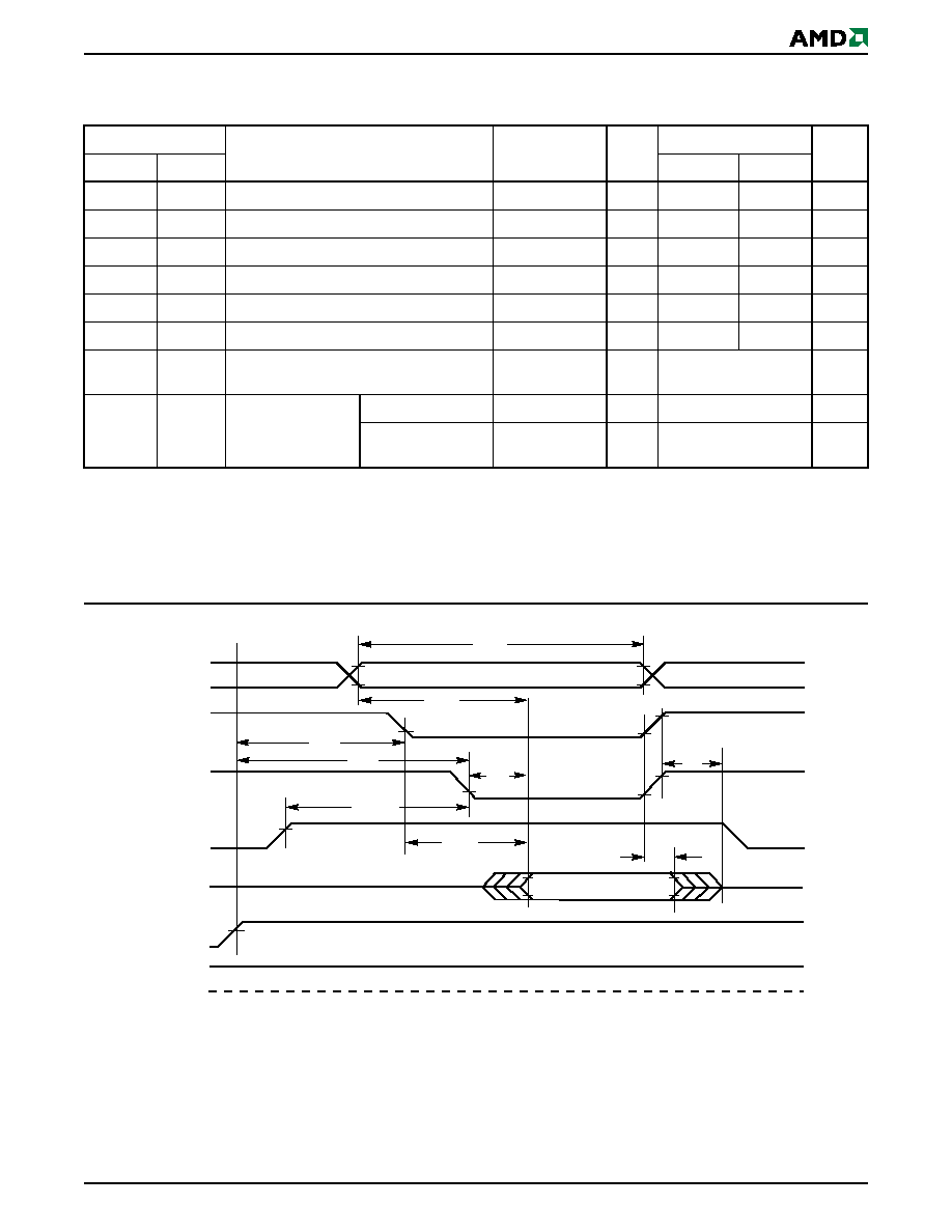
October 29, 2004
Am29LV652D
39
P R E L I M I N A R Y
AC CHARACTERISTICS
Read-Only Operations
Notes:
1. All test setups assume V
IO
= V
CC
.
2. Not 100% tested.
3. See
Figure 11, on page 38
and
Table 12, on page 38
for
test specifications
4. CE# can be replaced with CE2# when referring to the second device within the package.
.
Parameter
Description
Test Setup
(Note 1)
Speed Options
JEDEC
Std.
90R
12R
Unit
t
AVAV
t
RC
Read Cycle Time (Note 2)
Min
90
120
ns
t
AVQV
t
ACC
Address to Output Delay
CE#, OE# = V
IL
Max
90
120
ns
t
ELQV
t
CE
Chip Enable to Output Delay
OE# = V
IL
Max
90
120
ns
t
GLQV
t
OE
Output Enable to Output Delay
Max
35
50
ns
t
EHQZ
t
DF
Chip Enable to Output High Z (Note 2)
Max
30
30
ns
t
GHQZ
t
DF
Output Enable to Output High Z (Note 2)
Max
30
30
ns
t
AXQX
t
OH
Output Hold Time From Addresses, CE# or
OE#, Whichever Occurs First
Min
0
ns
t
OEH
Output Enable Hold
Time (Note 2)
Read
Min
0
ns
Toggle and
Data# Polling
Min
10
ns
t
OH
t
CE
Outputs
WE#
Addresses
CE# or CE2#
OE#
HIGH Z
Output Valid
HIGH Z
Addresses Stable
t
RC
t
ACC
t
OEH
t
RH
t
OE
t
RH
0 V
RY/BY#
RESET#
t
DF
Figure 13. Read Operation Timings
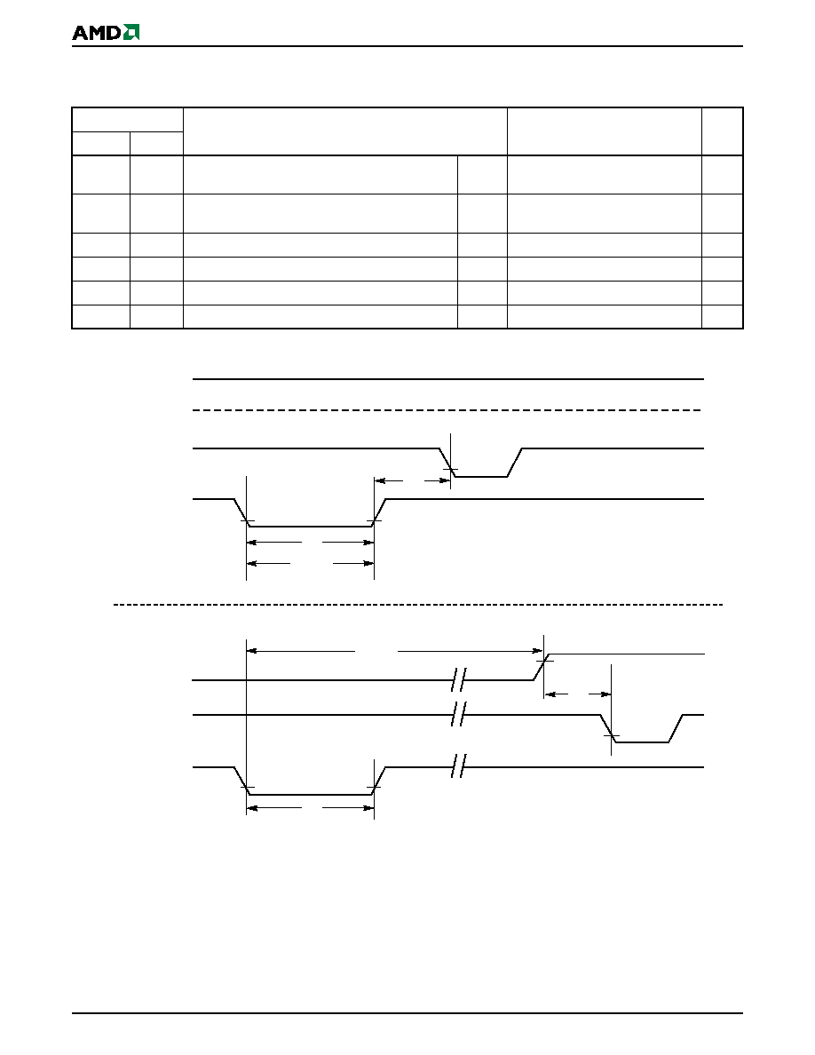
40
Am29LV652D
October 29, 2004
P R E L I M I N A R Y
AC CHARACTERISTICS
Hardware Reset (RESET#)
Note: Not 100% tested.
Parameter
Description
All Speed Options
Unit
JEDEC
Std
t
Ready
RESET# Pin Low (During Embedded Algorithms)
to Read Mode (See Note)
Max
20
µs
t
Ready
RESET# Pin Low (NOT During Embedded
Algorithms) to Read Mode (See Note)
Max
500
ns
t
RP
RESET# Pulse Width
Min
500
ns
t
RH
Reset High Time Before Read (See Note)
Min
50
ns
t
RPD
RESET# Low to Standby Mode
Min
20
µs
t
RB
RY/BY# Recovery Time
Min
0
ns
RESET#
RY/BY#
RY/BY#
t
RP
t
Ready
Reset Timings NOT during Embedded Algorithms
t
Ready
CE# or CE2#, OE#
t
RH
CE# or CE2#, OE#
Reset Timings during Embedded Algorithms
RESET#
t
RP
t
RB
Figure 14. Reset Timings
October 29, 2004
Am29LV652D
41
P R E L I M I N A R Y
AC CHARACTERISTICS
Erase and Program Operations
Notes:
1. Not 100% tested.
2. See the
"Erase And Programming Performance" on page 50
section for more information.
3. CE# can be replaced with CE2# when referring to the second device within the package.
Parameter
Speed Options
JEDEC
Std.
Description
90R
12R
Unit
t
AVAV
t
WC
Write Cycle Time (Note 1)
Min
90
120
ns
t
AVWL
t
AS
Address Setup Time
Min
0
ns
t
ASO
Address Setup Time to OE# low during toggle bit polling
Min
15
ns
t
WLAX
t
AH
Address Hold Time
Min
45
50
ns
t
AHT
Address Hold Time From CE# or OE# high
during toggle bit polling
Min
0
ns
t
DVWH
t
DS
Data Setup Time
Min
45
50
ns
t
WHDX
t
DH
Data Hold Time
Min
0
ns
t
OEPH
Output Enable High during toggle bit polling
Min
20
ns
t
GHWL
t
GHWL
Read Recovery Time Before Write
(OE# High to WE# Low)
Min
0
ns
t
ELWL
t
CS
CE# Setup Time
Min
0
ns
t
WHEH
t
CH
CE# Hold Time
Min
0
ns
t
WLWH
t
WP
Write Pulse Width
Min
35
50
ns
t
WHDL
t
WPH
Write Pulse Width High
Min
30
ns
t
WHWH1
t
WHWH1
Byte Programming Operation (Note 2)
Typ
5
µs
t
WHWH1
t
WHWH1
Accelerated Byte Programming Operation (Note 2)
Typ
4
µs
t
WHWH2
t
WHWH2
Sector Erase Operation (Note 2)
Typ
1.6
sec
t
VHH
V
HH
Rise and Fall Time (Note 1)
Min
250
ns
t
VCS
V
CC
Setup Time (Note 1)
Min
50
µs
t
RB
Write Recovery Time from RY/BY#
Min
0
ns
t
BUSY
Program/Erase Valid to RY/BY# Delay
Min
90
ns
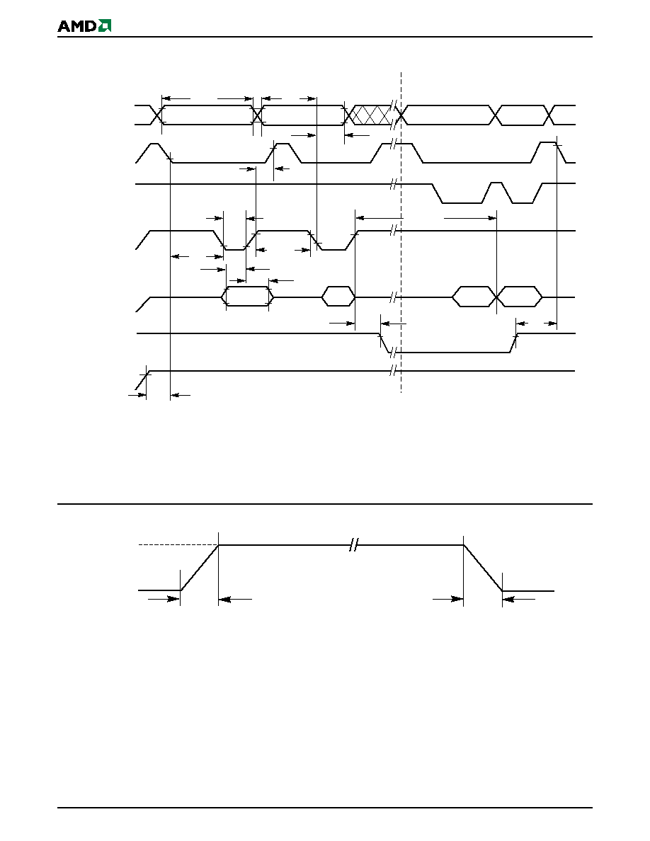
42
Am29LV652D
October 29, 2004
P R E L I M I N A R Y
AC CHARACTERISTICS
OE#
WE#
CE# or CE2#
V
CC
Data
Addresses
t
DS
t
AH
t
DH
t
WP
PD
t
WHWH1
t
WC
t
AS
t
WPH
t
VCS
XXXh
PA
PA
Read Status Data (last two cycles)
A0h
t
CS
Status
D
OUT
Program Command Sequence (last two cycles)
RY/BY#
t
RB
t
BUSY
t
CH
PA
Note: PA = program address, PD = program data, D
OUT
is the true data at the program address.
Figure 15. Program Operation Timings
ACC
t
VHH
V
HH
V
IL
or V
IH
V
IL
or V
IH
t
VHH
Figure 16. Accelerated Program Timing Diagram
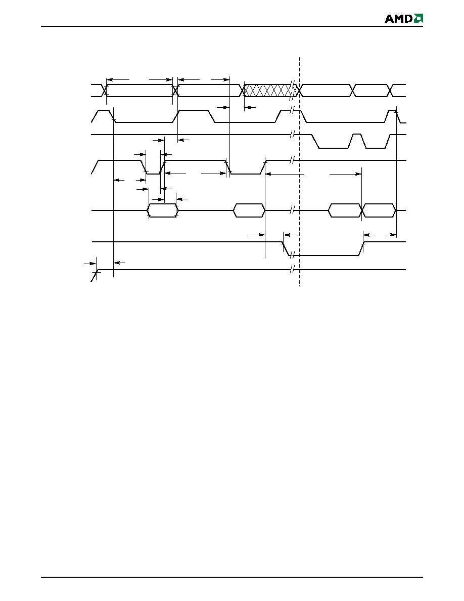
October 29, 2004
Am29LV652D
43
P R E L I M I N A R Y
AC CHARACTERISTICS
OE#
CE# or CE2#
Addresses
V
CC
WE#
Data
2AAh
SA
t
AH
t
WP
t
WC
t
AS
t
WPH
555 h for chip erase
10 for Chip Erase
30h
t
DS
t
VCS
t
CS
t
DH
55h
t
CH
In
Progress
Complete
t
WHWH2
VA
VA
Erase Command Sequence (last two cycles)
Read Status Data
RY/BY#
t
RB
t
BUSY
Note: SA = sector address (for Sector Erase), VA = Valid Address for reading status data (see
"Write Operation Status" on page 31
.
Figure 17. Chip/Sector Erase Operation Timings
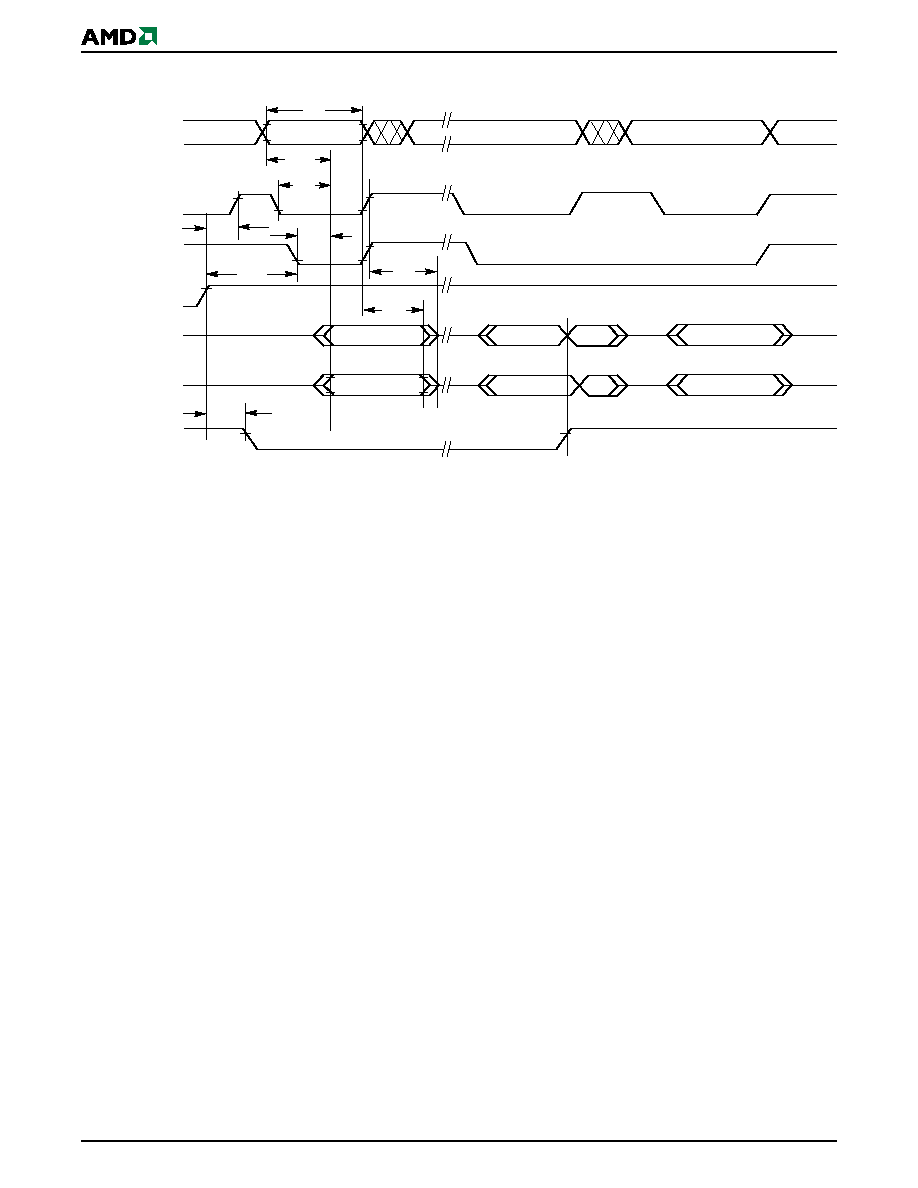
44
Am29LV652D
October 29, 2004
P R E L I M I N A R Y
AC CHARACTERISTICS
WE#
CE# or CE2#
OE#
High Z
t
OE
High Z
DQ7
DQ0≠DQ6
RY/BY#
t
BUSY
Complement
True
Addresses
VA
t
OEH
t
CE
t
CH
t
OH
t
DF
VA
VA
Status Data
Complement
Status Data
True
Valid Data
Valid Data
t
ACC
t
RC
Note: VA = Valid address. Illustration shows first status cycle after command sequence, last status read cycle, and array data
read cycle.
Figure 18. Data# Polling Timings (During Embedded Algorithms)
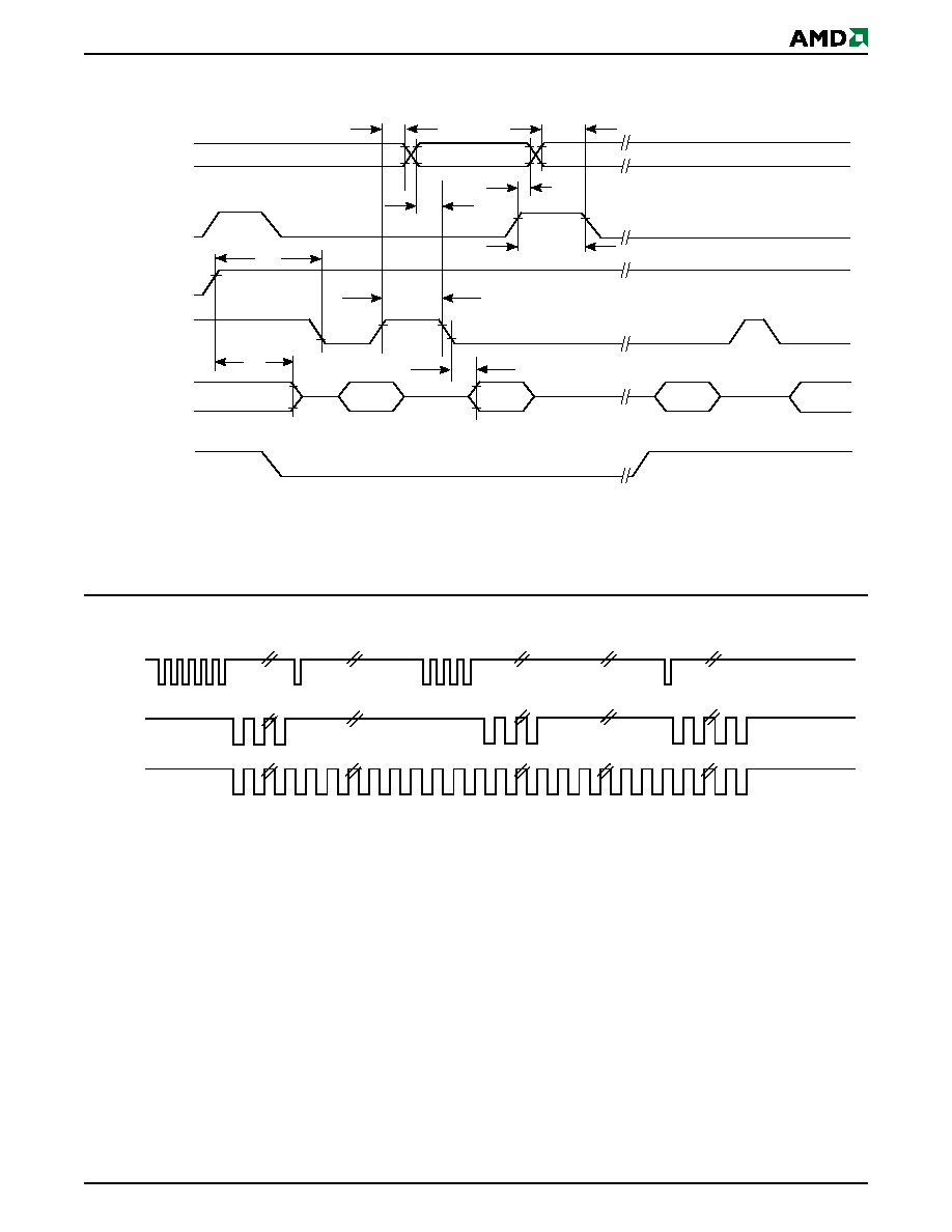
October 29, 2004
Am29LV652D
45
P R E L I M I N A R Y
AC CHARACTERISTICS
OE#
CE# or CE2#
WE#
Addresses
t
OEH
t
DH
t
AHT
t
ASO
t
OEPH
t
OE
Valid Data
(first read)
(second read)
(stops toggling)
t
CEPH
t
AHT
t
AS
DQ6/DQ2
Valid Data
Valid
Status
Valid
Status
Valid
Status
RY/BY#
Note: VA = Valid address; not required for DQ6. Illustration shows first two status cycle after command sequence, last status
read cycle, and array data read cycle
Figure 19. Toggle Bit Timings (During Embedded Algorithms)
Note: DQ2 toggles only when read at an address within an erase-suspended sector. The system may use OE# or CE# to toggle
DQ2 and DQ6.
Figure 20. DQ2 vs. DQ6
Enter
Erase
Erase
Erase
Enter Erase
Suspend Program
Erase Suspend
Read
Erase Suspend
Read
Erase
WE#
DQ6
DQ2
Erase
Complete
Erase
Suspend
Suspend
Program
Resume
Embedded
Erasing
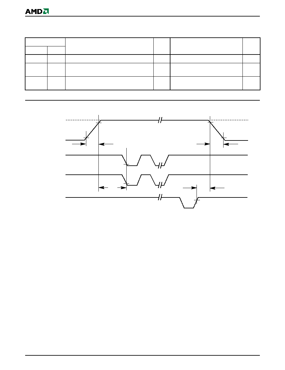
46
Am29LV652D
October 29, 2004
P R E L I M I N A R Y
AC CHARACTERISTICS
Temporary Sector Unprotect
Note: Not 100% tested.
Parameter
All Speed Options
JEDEC
Std
Description
Unit
t
VIDR
V
ID
Rise and Fall Time (See Note)
Min
500
ns
t
RSP
RESET# Setup Time for Temporary Sector
Unprotect
Min
4
µs
t
RRB
RESET# Hold Time from RY/BY# High for
Temporary Sector Group Unprotect
Min
4
µs
RESET#
t
VIDR
V
ID
V
SS
, V
IL
,
or V
IH
V
ID
V
SS
, V
IL
,
or V
IH
CE# or CE2#
WE#
RY/BY#
t
VIDR
t
RSP
Program or Erase Command Sequence
t
RRB
Figure 21. Temporary Sector Group Unprotect Timing Diagram

October 29, 2004
Am29LV652D
47
P R E L I M I N A R Y
AC CHARACTERISTICS
Sector Group Protect: 150 µs
Sector Group Unprotect: 15 ms
1 µs
RESET#
SA, A6,
A1, A0
Data
CE# or CE2#
WE#
OE#
60h
60h
40h
Valid*
Valid*
Valid*
Status
Sector Group Protect/Unprotect
Verify
V
ID
V
IH
* For sector group protect, A6 = 0, A1 = 1, A0 = 0. For sector group unprotect, A6 = 1, A1 = 1, A0 = 0.
Figure 22. Sector Group Protect and Unprotect Timing Diagram

48
Am29LV652D
October 29, 2004
P R E L I M I N A R Y
AC CHARACTERISTICS
Alternate CE# Controlled Erase and Program Operations
Notes:
1. Not 100% tested.
2. See the "Erase And Programming Performance" section for more information.
3. CE# can be replaced with CE2# when referring to the second device within the package.
Parameter
Speed Options
JEDEC
Std
Description
90R
12R
Unit
t
AVAV
t
WC
Write Cycle Time (Note 1)
Min
90
120
ns
t
AVWL
t
AS
Address Setup Time
Min
0
ns
t
ELAX
t
AH
Address Hold Time
Min
45
50
ns
t
DVEH
t
DS
Data Setup Time
Min
45
50
ns
t
EHDX
t
DH
Data Hold Time
Min
0
ns
t
GHEL
t
GHEL
Read Recovery Time Before Write
(OE# High to WE# Low)
Min
0
ns
t
WLEL
t
WS
WE# Setup Time
Min
0
ns
t
EHWH
t
WH
WE# Hold Time
Min
0
ns
t
ELEH
t
CP
CE# Pulse Width
Min
45
50
ns
t
EHEL
t
CPH
CE# Pulse Width High
Min
30
ns
t
WHWH1
t
WHWH1
Byte Programming Operation (Note 2)
Typ
5
µs
t
WHWH1
t
WHWH1
Accelerated Byte Programming Operation (Note 2)
Typ
4
µs
t
WHWH2
t
WHWH2
Sector Erase Operation (Note 2)
Typ
1.6
sec
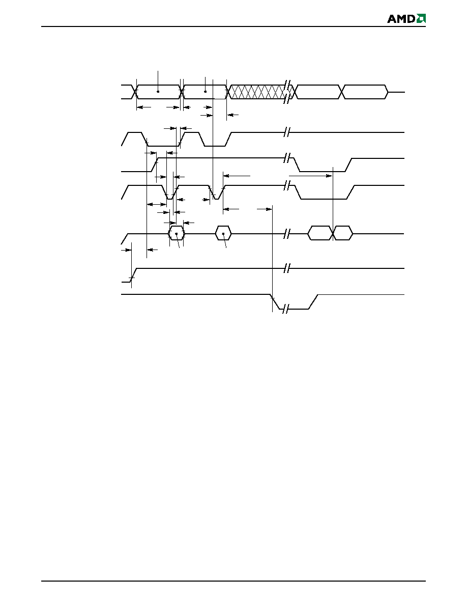
October 29, 2004
Am29LV652D
49
P R E L I M I N A R Y
AC CHARACTERISTICS
t
GHEL
t
WS
OE#
CE# or CE2#
WE#
RESET#
t
DS
Data
t
AH
Addresses
t
DH
t
CP
DQ7#
D
OUT
t
WC
t
AS
t
CPH
PA
Data# Polling
A0 for program
55 for erase
t
RH
t
WHWH1 or 2
RY/BY#
t
WH
PD for program
30 for sector erase
10 for chip erase
555 for program
2AA for erase
PA for program
SA for sector erase
555 for chip erase
t
BUSY
Notes:
1. Figure indicates last two bus cycles of a program or erase operation.
2. PA = program address, SA = sector address, PD = program data.
3. DQ7# is the complement of the data written to the device. D
OUT
is the data written to the device.
Figure 23. Alternate CE# Controlled Write (Erase/Program) Operation Timings
50
Am29LV652D
October 29, 2004
P R E L I M I N A R Y
ERASE AND PROGRAMMING PERFORMANCE
Notes:
1. Typical program and erase times assume the following conditions: 25
∞C, 3.0 V V
CC
, 1,000,000 cycles. Additionally,
programming typicals assume checkerboard pattern.
2. Under worst case conditions of 90
∞C, V
CC
= 3.0 V, 1,000,000 cycles.
3. The typical chip programming time is considerably less than the maximum chip programming time listed, since most bytes
program faster than the maximum program times listed.
4. In the pre-programming step of the Embedded Erase algorithm, all bits are programmed to 00h before erasure.
5. System-level overhead is the time required to execute the two- or four-bus-cycle sequence for the program command. See
Table 10, on page 30
for further information on command definitions.
6. The device has a minimum erase and program cycle endurance of 1,000,000 cycles.
LATCHUP CHARACTERISTICS
Note: Includes all connections except V
CC
. Test conditions: V
CC
= 3.0 V, one connection at a time.
INPUT/OUTPUT CAPACITANCE
Notes:
1. Sampled, not 100% tested.
2. Test conditions T
A
= 25∞C, f = 1.0 MHz.
DATA RETENTION
Parameter
Typ (Note 1)
Max (Note 2)
Unit
Comments
Sector Erase Time
1.6
15
sec
Excludes 00h programming
prior to erasure (Note 4)
Chip Erase Time
205
sec
Byte Program Time
5
150
µs
Excludes system level
overhead (Note 5)
Accelerated Byte Program Time
4
120
µs
Chip Program Time (Note 3)
42
126
sec
Description
Min
Max
Input voltage with respect to V
SS
on all device connections (including
A9, OE#, and RESET#) except I/Os
≠1.0 V
12.5 V
Input voltage with respect to V
SS
on all I/Os
≠1.0 V
V
CC
+ 1.0 V
V
CC
Current
≠100 mA
+100 mA
Parameter
Symbol
Parameter Description
Test Setup
Typ
Max
Unit
C
IN
Input Capacitance
V
IN
= 0
12
16
pF
C
OUT
Output Capacitance
V
OUT
= 0
12
16
pF
C
E
/C
E2
Control Pin Capacitance
V
IN
= 0
6
8
pF
Parameter Description
Test Conditions
Min
Unit
Minimum Pattern Data Retention Time
150
∞C
10
Years
125
∞C
20
Years

October 29, 2004
Am29LV652D
51
P R E L I M I N A R Y
PHYSICAL DIMENSIONS
FSA063--63-Ball Fine-Pitch Ball Grid Array (FBGA) 11 x 12 mm package

52
Am29LV652D
October 29, 2004
P R E L I M I N A R Y
REVISION SUMMARY
Revision A (May 24, 2001)
Initial release.
Revision A+1 (July 31, 2001)
AC Characteristics--Alternate CE# Controlled
Erase and Program Table
t
WHWH1
--Byte Programming Operation: Changed typi-
cal value from 11 µs to 5 µs.
t
WHWH1
--Accelerated Byte Programming Operation:
Changed typical value from 7 µs to 4 µs.
Revision A+2 (August 14, 2001)
Global
Removed the speed options for 100 ns with V
IO
= 1.8
V ≠ 2.9 V and 120 ns with V
IO
= 1.8 V ≠ 2.9 V.
Changed the speed option for 120 ns with V
IO
= 3.0 V
≠ 5.0 V from 120R to 12R.
General Description and Device Bus Operations
Added "For voltage levels below 3 V, contact an AMD
representative for more information." to VersatileI/OTM
text.
Ordering Information
Removed the Optional Processing from the order
number.
Revision A+3 (January 10, 2002)
Global
Clarified description of VersatileIO (V
IO
) in the follow-
ing sections: Distinctive Characteristics; General De-
scription; VersatileIO (V
IO
) Control; Operating Ranges;
DC Characteristics; CMOS compatible.
Revision A+4 (October 29, 2004
Global
Added Spansion Cover Sheet
Added reference links to page numbers
Added Colophon
Ordering Information
Added two package types to temperature range.
Valid Combination for FBGA Packages
Added MAF and MAK to order number.
Added F and K to Package Marking.

53
Am29LV652D
October 29, 2004
P R E L I M I N A R Y
Colophon
The products described in this document are designed, developed and manufactured as contemplated for general use, including without limita-
tion, ordinary industrial use, general office use, personal use, and household use, but are not designed, developed and manufactured as con-
templated (1) for
any
use
that includes
fatal risks or dangers that, unless extremely high safety is secured, could have a serious effect to the
public, and could lead directly to death, personal injury, severe physical damage or other loss (i.e., nuclear reaction control in nuclear facility,
aircraft flight control, air traffic control, mass transport control, medical life support system, missile launch control in weapon system), or (2)
for
any use where chance of failure is intolerable
(i.e., submersible repeater and artificial satellite). Please note that Spansion LLC will not be liable
to
you and/or any third party for any claims or damages arising in connection with above-mentioned uses of the products. Any semiconductor
devices have an inherent chance of failure. You must protect against injury, damage or loss from such failures by incorporating safety design
measures into your facility and equipment such as redundancy, fire protection, and prevention of over-current levels and other abnormal operat-
ing conditions. If any products described in this document represent goods or technologies subject to certain restrictions on export under the
Foreign Exchange and Foreign Trade Law of Japan
, the US Export Administration Regulations or the applicable laws of any other country,
the
prior authorization by
the respective government entity
will be required for export of those product
Trademarks
Copyright © 2000
-2004
Advanced Micro Devices, Inc. All rights reserved.
AMD, the AMD logo, and combinations thereof are registered trademarks of Advanced Micro Devices, Inc.
ExpressFlash is a trademark of Advanced Micro Devices, Inc.
Product names used in this publication are for identification purposes only and may be trademarks of their respective companies