
-XO\
7KH IROORZLQJ GRFXPHQW VSHFLILHV 6SDQVLRQ PHPRU\ SURGXFWV WKDW DUH QRZ RIIHUHG E\ ERWK $GYDQFHG
0LFUR 'HYLFHV DQG )XMLWVX $OWKRXJK WKH GRFXPHQW LV PDUNHG ZLWK WKH QDPH RI WKH FRPSDQ\ WKDW RULJ
LQDOO\ GHYHORSHG WKH VSHFLILFDWLRQ WKHVH SURGXFWV ZLOO EH RIIHUHG WR FXVWRPHUV RI ERWK $0' DQG
)XMLWVX
Continuity of Specifications
7KHUH LV QR FKDQJH WR WKLV GDWDVKHHW DV D UHVXOW RI RIIHULQJ WKH GHYLFH DV D 6SDQVLRQ SURGXFW $Q\
FKDQJHV WKDW KDYH EHHQ PDGH DUH WKH UHVXOW RI QRUPDO GDWDVKHHW LPSURYHPHQW DQG DUH QRWHG LQ WKH
GRFXPHQW UHYLVLRQ VXPPDU\ ZKHUH VXSSRUWHG )XWXUH URXWLQH UHYLVLRQV ZLOO RFFXU ZKHQ DSSURSULDWH
DQG FKDQJHV ZLOO EH QRWHG LQ D UHYLVLRQ VXPPDU\
Continuity of Ordering Part Numbers
$0' DQG )XMLWVX FRQWLQXH WR VXSSRUW H[LVWLQJ SDUW QXPEHUV EHJLQQLQJ ZLWK ≥$P¥ DQG ≥0%0¥ 7R RUGHU
WKHVH SURGXFWV SOHDVH XVH RQO\ WKH 2UGHULQJ 3DUW 1XPEHUV OLVWHG LQ WKLV GRFXPHQW
For More Information
3OHDVH FRQWDFW \RXU ORFDO $0' RU )XMLWVX VDOHV RIILFH IRU DGGLWLRQDO LQIRUPDWLRQ DERXW 6SDQVLRQ
PHPRU\ VROXWLRQV
Am29PDL127H
Data Sheet
Publication Number 26864 Revision
A
Amendment +4 Issue Date June 30, 2003

THIS PAGE LEFT INTENTIONALLY BLANK.

ADVANCE INFORMATION
This document contains information on a product under development at Advanced Micro Devices. The information
is intended to help you evaluate this product. AMD reserves the right to change or discontinue work on this proposed
product without notice.
Publication# 26864 Rev: A Amendment/+4
Issue Date: June 30, 2003
Am29PDL127H
128 Megabit (8 M x 16-Bit) CMOS 3.0 Volt-only, Page Mode Simultaneous Read/Write
Flash Memory with Enhanced VersatileIO
TM
Control
DISTINCTIVE CHARACTERISTICS
ARCHITECTURAL ADVANTAGES
128 Mbit Page Mode device
-- Page size of 8 words: Fast page read access from random
locations within the page
Single power supply operation
-- Full Voltage range: 2.7 to 3.6 volt read, erase, and program
operations for battery-powered applications
Simultaneous Read/Write Operation
-- Data can be continuously read from one bank while
executing erase/program functions in another bank
-- Zero latency switching from write to read operations
FlexBank Architecture
-- 4 separate banks, with up to two simultaneous operations
per device
-- Bank A: 16 Mbit (4 Kw x 8 and 32 Kw x 31)
-- Bank B: 48 Mbit (32 Kw x 96)
-- Bank C: 48 Mbit (32 Kw x 96)
-- Bank D: 16 Mbit (4 Kw x 8 and 32 Kw x 31)
Enhanced VersatileI/O
TM
(V
IO
) Control
-- Output voltage generated and input voltages tolerated on all
control inputs and I/Os is determined by the voltage on the
V
IO
pin
-- V
IO
options at 1.8 V and 3 V I/O
SecSi
TM
(Secured Silicon) Sector region
-- Up to 128 words accessible through a command sequence
-- Up to 64 factory-locked words
-- Up to 64 customer-lockable words
Both top and bottom boot blocks in one device
Manufactured on 0.13 µm process technology
20-year data retention at 125∞C
Minimum 1 million erase cycle guarantee per sector
PERFORMANCE CHARACTERISTICS
High Performance
-- Page access times as fast as 20 ns
-- Random access times as fast as 55 ns
Power consumption (typical values at 10 MHz)
-- 55 mA active read current
-- 25 mA program/erase current
-- 1 µA typical standby mode current
SOFTWARE FEATURES
Software command-set compatible with JEDEC 42.4
standard
-- Backward compatible with Am29F and Am29LV families
CFI (Common Flash Interface) complaint
-- Provides device-specific information to the system, allowing
host software to easily reconfigure for different Flash devices
Erase Suspend / Erase Resume
-- Suspends an erase operation to allow read or program
operations in other sectors of same bank
Unlock Bypass Program command
-- Reduces overall programming time when issuing multiple
program command sequences
HARDWARE FEATURES
Ready/Busy# pin (RY/BY#)
-- Provides a hardware method of detecting program or erase
cycle completion
Hardware reset pin (RESET#)
-- Hardware method to reset the device to reading array data
WP#/ ACC (Write Protect/Acceleration) input
-- At V
IL
, hardware level protection for the first and last two 4K
word sectors.
-- At V
IH
, allows removal of sector protection
-- At V
HH
, provides accelerated programming in a factory
setting
Persistent Sector Protection
-- A command sector protection method to lock combinations
of individual sectors and sector groups to prevent program or
erase operations within that sector
-- Sectors can be locked and unlocked in-system at V
CC
level
Password Sector Protection
-- A sophisticated sector protection method to lock
combinations of individual sectors and sector groups to
prevent program or erase operations within that sector using
a user-defined 64-bit password
Package options
-- 64-ball Fortified BGA
-- 80-ball Fine-pitch BGA
-- Multi Chip Packages (MCP)
2
Am29PDL127H
June 30, 2003
A D V A N C E I N F O R M A T I O N
GENERAL DESCRIPTION
The Am29PDL127H is a 128 Mbit, 3.0 volt-only Page Mode
and Simultaneous Read/Write Flash memory device orga-
nized as 8 Mwords. The device is offered in a 64-ball Forti-
fied BGA package, an 80-ball Fine-pitch BGA package, and
various multi-chip packages. The word-wide data (x16) ap-
pears on DQ15-DQ0. This device can be programmed
in-system or in standard EPROM programmers. A 12.0 V
V
PP
is not required for write or erase operations.
The device offers fast page access times of 20 to 30 ns, with
corresponding random access times of 55 to 85 ns, respec-
tively, allowing high speed microprocessors to operate with-
out wait states. To eliminate bus contention the device has
separate chip enable (CE#), write enable (WE#) and output
enable (OE#) controls. Simultaneous Read/Write Operation
with Zero Latency
The Simultaneous Read/Write architecture provides simul-
taneous operation by dividing the memory space into 4
banks, which can be considered to be four separate memory
arrays as far as certain operations are concerned. The de-
vice can improve overall system performance by allowing a
host system to program or erase in one bank, then immedi-
ately and simultaneously read from another bank with zero
latency (with two simultaneous operations operating at any
one time). This releases the system from waiting for the
completion of a program or erase operation, greatly improv-
ing system performance.
The device can be organized in both top and bottom sector
configurations. The banks are organized as follows:
Page Mode Features
The page size is 8 words. After initial page access is accom-
plished, the page mode operation provides fast read access
speed of random locations within that page.
Standard Flash Memory Features
The device requires a single 3.0 volt power supply (2.7 V
to 3.6 V or 2.7 V to 3.3 V) for both read and write functions.
Internally generated and regulated voltages are provided for
the program and erase operations.
The device is entirely command set compatible with the
JEDEC 42.4 single-power-supply Flash standard. Com-
mands are written to the command register using standard
microprocessor write timing. Register contents serve as in-
puts to an internal state-machine that controls the erase and
programming circuitry. Write cycles also internally latch ad-
dresses and data needed for the programming and erase
operations. Reading data out of the device is similar to read-
ing from other Flash or EPROM devices.
Device programming occurs by executing the program com-
mand sequence. The Unlock Bypass mode facilitates faster
programming times by requiring only two write cycles to pro-
gram data instead of four. Device erasure occurs by execut-
ing the erase command sequence.
The host system can detect whether a program or erase op-
eration is complete by reading the DQ7 (Data# Polling) and
DQ6 (toggle) status bits. After a program or erase cycle has
been completed, the device is ready to read array data or
accept another command.
The sector erase architecture allows memory sectors to be
erased and reprogrammed without affecting the data con-
tents of other sectors. The device is fully erased when
shipped from the factory.
Hardware data protection measures include a low V
CC
de-
tector that automatically inhibits write operations during
power transitions. The hardware sector protection feature
disables both program and erase operations in any combi-
nation of sectors of memory. This can be achieved in-system
or via programming equipment.
The Erase Suspend/Erase Resume feature enables the
user to put erase on hold for any period of time to read data
from, or program data to, any sector that is not selected for
erasure. True background erase can thus be achieved. If a
read is needed from the SecSi Sector area (One Time Pro-
gram area) after an erase suspend, then the user must use
the proper command sequence to enter and exit this region.
The device offers two power-saving features. When ad-
dresses have been stable for a specified amount of time, the
device enters the automatic sleep mode. The system can
also place the device into the standby mode. Power con-
sumption is greatly reduced in both these modes.
AMD's Flash technology combined years of Flash memory
manufacturing experience to produce the highest levels of
quality, reliability and cost effectiveness. The device electri-
cally erases all bits within a sector simultaneously via
Fowler-Nordheim tunneling. The data is programmed using
hot electron injection.
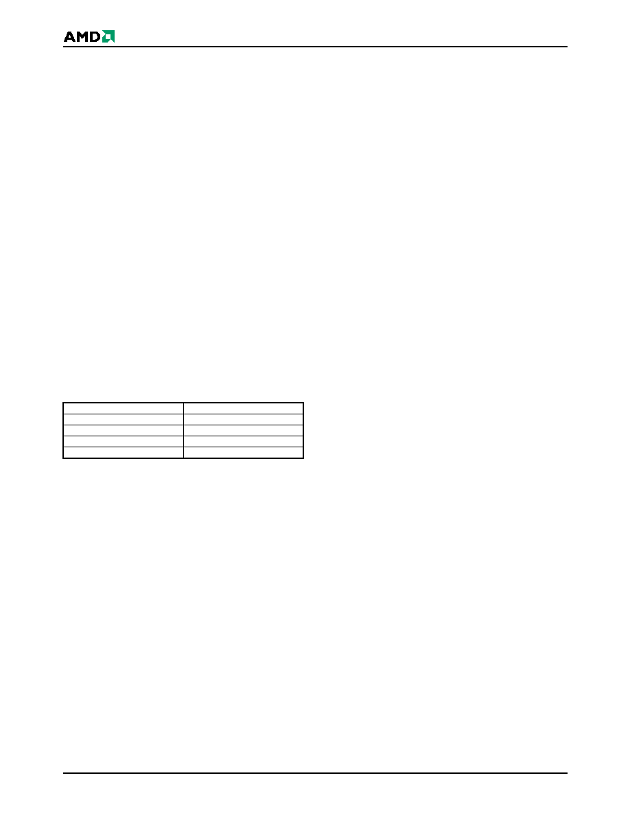
Bank
Sectors
A
16 Mbit (4 Kw x 8 and 32 Kw x 31)
B
48 Mbit (32 Kw x 96)
C
48 Mbit (32 Kw x 96)
D
16 Mbit (4 Kw x 8 and 32 Kw x 31)

June 30, 2003
Am29PDL127H
3
A D V A N C E I N F O R M A T I O N
TABLE OF CONTENTS
Product Selector Guide . . . . . . . . . . . . . . . . . . . . . 5
Block Diagram . . . . . . . . . . . . . . . . . . . . . . . . . . . . 5
Simultaneous Operation Block Diagram . . . . . . . 6
Connection Diagrams . . . . . . . . . . . . . . . . . . . . . . 7
Pin Description. . . . . . . . . . . . . . . . . . . . . . . . . . . . 9
Ordering Information . . . . . . . . . . . . . . . . . . . . . . 10
Device Bus Operations . . . . . . . . . . . . . . . . . . . . 11
Table 1. Am29PDL127H Device Bus Operations ...........................11
Requirements for Reading Array Data ................................... 11
Random Read (Non-Page Read) ........................................... 11
Page Mode Read .................................................................... 11
Table 2. Page Select .......................................................................12
Simultaneous Operation ......................................................... 12
Table 3. Bank Select .......................................................................12
Writing Commands/Command Sequences ............................ 12
Accelerated Program Operation ............................................. 12
Autoselect Functions .............................................................. 12
Automatic Sleep Mode ........................................................... 13
RESET#: Hardware Reset Pin ............................................... 13
Output Disable Mode .............................................................. 13
Table 4. Am29PDL127H Sector Architecture ..................................14
Table 5. SecSi
TM
Sector Addresses ...............................................21
Table 6. Autoselect Codes (High Voltage Method) ........................22
Table 7. Am29PDL127H Boot Sector/Sector Block Addresses for
Protection/Unprotection ...................................................................23
Sector Protection . . . . . . . . . . . . . . . . . . . . . . . . . 24
Persistent Sector Protection ................................................... 24
Persistent Protection Bit (PPB) ............................................... 24
Persistent Protection Bit Lock (PPB Lock) ............................. 24
Dynamic Protection Bit (DYB) ................................................ 24
Table 8. Sector Protection Schemes ...............................................25
Persistent Sector Protection Mode Locking Bit ...................... 25
Password Protection Mode ..................................................... 25
Password and Password Mode Locking Bit ........................... 26
64-bit Password ...................................................................... 26
Write Protect (WP#) ................................................................ 26
Persistent Protection Bit Lock ................................................. 26
High Voltage Sector Protection .............................................. 27
Figure 1. In-System Sector Protection/
Sector Unprotection Algorithms ...................................................... 28
Temporary Sector Unprotect .................................................. 29
Figure 2. Temporary Sector Unprotect Operation........................... 29
SecSiTM (Secured Silicon) Sector
Flash Memory Region ............................................................ 29
Factory-Locked Area (64 words) ............................................ 29
Customer-Lockable Area (64 words) ...................................... 29
SecSi Sector Protection Bits ................................................... 30
Figure 3. SecSi Sector Protect Verify.............................................. 30
Hardware Data Protection ...................................................... 30
Low VCC Write Inhibit ............................................................ 30
Write Pulse "Glitch" Protection ............................................... 30
Logical Inhibit .......................................................................... 30
Power-Up Write Inhibit ............................................................ 30
Common Flash Memory Interface (CFI) . . . . . . . 30
Command Definitions . . . . . . . . . . . . . . . . . . . . . 34
Reading Array Data ................................................................ 34
Reset Command ..................................................................... 34
Autoselect Command Sequence ............................................ 34
Enter SecSiTM Sector/Exit SecSi Sector
Command Sequence .............................................................. 34
Word Program Command Sequence ...................................... 35
Unlock Bypass Command Sequence ..................................... 35
Figure 4. Program Operation ......................................................... 36
Chip Erase Command Sequence ........................................... 36
Sector Erase Command Sequence ........................................ 36
Figure 5. Erase Operation.............................................................. 37
Erase Suspend/Erase Resume Commands ........................... 37
Password Program Command ................................................ 37
Password Verify Command .................................................... 38
Password Protection Mode Locking Bit Program Command .. 38
Persistent Sector Protection Mode Locking Bit Program
Command ............................................................................... 38
SecSi Sector Protection Bit Program Command .................... 38
PPB Lock Bit Set Command ................................................... 38
DYB Write Command ............................................................. 38
Password Unlock Command .................................................. 39
PPB Program Command ........................................................ 39
All PPB Erase Command ........................................................ 39
DYB Write Command ............................................................. 39
PPB Lock Bit Set Command ................................................... 39
PPB Status Command ............................................................ 39
PPB Lock Bit Status Command .............................................. 39
Sector Protection Status Command ....................................... 39
Table 13. Memory Array Command Definitions ............................. 40
Table 14. Sector Protection Command Definitions ........................ 41
Write Operation Status . . . . . . . . . . . . . . . . . . . . . 42
DQ7: Data# Polling ................................................................. 42
Figure 6. Data# Polling Algorithm .................................................. 42
DQ6: Toggle Bit I .................................................................... 43
Figure 7. Toggle Bit Algorithm........................................................ 43
DQ2: Toggle Bit II ................................................................... 44
Reading Toggle Bits DQ6/DQ2 ............................................... 44
DQ5: Exceeded Timing Limits ................................................ 44
DQ3: Sector Erase Timer ....................................................... 44
Table 15. Write Operation Status ................................................... 45
Absolute Maximum Ratings. . . . . . . . . . . . . . . . . 46
Figure 8. Maximum Negative Overshoot Waveform ...................... 46
Figure 9. Maximum Positive Overshoot Waveform........................ 46
DC Characteristics . . . . . . . . . . . . . . . . . . . . . . . . 47
Test Conditions. . . . . . . . . . . . . . . . . . . . . . . . . . . 48
Figure 10. Test Setup.................................................................... 48
Figure 11. Input Waveforms and Measurement Levels ................. 48
AC Characteristic . . . . . . . . . . . . . . . . . . . . . . . . . 49
Read-Only Operations ........................................................... 49
Figure 12. Read Operation Timings ............................................... 50
Figure 13. Page Read Operation Timings...................................... 50
Hardware Reset (RESET#) .................................................... 51
Figure 14. Reset Timings ............................................................... 51
Erase and Program Operations .............................................. 52
Figure 15. Program Operation Timings.......................................... 53
Figure 16. Accelerated Program Timing Diagram .......................... 53
Figure 17. Chip/Sector Erase Operation Timings .......................... 54
Figure 18. Back-to-back Read/Write Cycle Timings ...................... 55
Figure 19. Data# Polling Timings (During Embedded Algorithms). 55
Figure 20. Toggle Bit Timings (During Embedded Algorithms)...... 56