ńÓÍůžŚŪÚŗŲŤˇ Ť ÓÔŤŮŗŪŤˇ www.docs.chipfind.ru

-XO\
7KH IROORZLQJ GRFXPHQW VSHFLILHV 6SDQVLRQ PHPRU\ SURGXFWV WKDW DUH QRZ RIIHUHG E\ ERWK $GYDQFHG
0LFUR 'HYLFHV DQG )XMLWVX $OWKRXJK WKH GRFXPHQW LV PDUNHG ZLWK WKH QDPH RI WKH FRPSDQ\ WKDW RULJ
LQDOO\ GHYHORSHG WKH VSHFLILFDWLRQ WKHVH SURGXFWV ZLOO EH RIIHUHG WR FXVWRPHUV RI ERWK $0' DQG
)XMLWVX
Continuity of Specifications
7KHUH LV QR FKDQJH WR WKLV GDWDVKHHW DV D UHVXOW RI RIIHULQJ WKH GHYLFH DV D 6SDQVLRQ SURGXFW $Q\
FKDQJHV WKDW KDYH EHHQ PDGH DUH WKH UHVXOW RI QRUPDO GDWDVKHHW LPSURYHPHQW DQG DUH QRWHG LQ WKH
GRFXPHQW UHYLVLRQ VXPPDU\ ZKHUH VXSSRUWHG )XWXUH URXWLQH UHYLVLRQV ZLOO RFFXU ZKHQ DSSURSULDWH
DQG FKDQJHV ZLOO EH QRWHG LQ D UHYLVLRQ VXPPDU\
Continuity of Ordering Part Numbers
$0' DQG )XMLWVX FRQWLQXH WR VXSSRUW H[LVWLQJ SDUW QXPEHUV EHJLQQLQJ ZLWK ≥$Pī DQG ≥0%0ī 7R RUGHU
WKHVH SURGXFWV SOHDVH XVH RQO\ WKH 2UGHULQJ 3DUW 1XPEHUV OLVWHG LQ WKLV GRFXPHQW
For More Information
3OHDVH FRQWDFW \RXU ORFDO $0' RU )XMLWVX VDOHV RIILFH IRU DGGLWLRQDO LQIRUPDWLRQ DERXW 6SDQVLRQ
PHPRU\ VROXWLRQV
Am42BDS640AG
Data Sheet
Publication Number 26445 Revision
B
Amendment 0 Issue
Date
November 1, 2002

PRELIMINARY
This document contains information on a product under development at Advanced Micro Devices. The information
is intended to help you evaluate this product. AMD reserves the right to change or discontinue work on this proposed
product without notice.
Publication# 26445
Rev: B Amendment/0
Issue Date: November 1, 2002
Refer to AMD's Website (www.amd.com) for the latest information.
Am42BDS640AG
Stacked Multi-Chip Package (MCP) Flash Memory and SRAM
Am29BDS640G 64 Megabit (4 M x 16-Bit) CMOS 1.8 Volt-only, Simultaneous Operation,
Burst Mode Flash Memory and 16 Mbit (1 M x 16-Bit) Static RAM
DISTINCTIVE CHARACTERISTICS
MCP Features
Power supply voltage of 1.65 to 1.95 volt
High performance
-- Access time as fast as 70 ns
Package
-- 93-Ball FBGA
Operating Temperature
-- ≠40įC to +85įC
Flash Memory Features
ARCHITECTURAL ADVANTAGES
Single 1.8 volt read, program and erase (1.65 to 1.95 volt)
Manufactured on 0.17 Ķm process technology
Simultaneous Read/Write operation
-- Data can be continuously read from one bank while
executing erase/program functions in other bank
-- Zero latency between read and write operations
-- Four bank architecture: 16Mb/16Mb/16Mb/16Mb
Programmable Burst Interface
-- 2 Modes of Burst Read Operation
-- Linear Burst: 8, 16, and 32 words with wrap-around
-- Continuous Sequential Burst
Sector Architecture
-- Eight 8 Kword sectors and one hundred twenty-six 32
Kword sectors
-- Banks A and D each contain four 8 Kword sectors and
thirty-one 32 Kword sectors; Banks B and C each contain
thirty-two 32 Kword sectors
-- Eight 8 Kword boot sectors, four at the top of the address
range, and four at the bottom of the address range
Minimum 1 million erase cycle guarantee per sector
20-year data retention at 125įC
PERFORMANCE CHARCTERISTICS
Read access times at 54/40 MHz
-- Burst access times of 13.5/20 ns @ 30 pF at industrial
temperature range
-- Asynchronous random access times of 70 ns (at 30 pF)
-- Synchronous latency of 87.5/95 ns
Power dissipation (typical values, C
L
= 30 pF)
-- Burst Mode Read: 10 mA
-- Simultaneous Operation: 25 mA
-- Program/Erase: 15 mA
-- Standby mode: 0.2 ĶA
HARDWARE FEATURES
Software command sector locking
Handshaking: host monitors operations via RDY output
Hardware reset input (RESET#)
WP# input
-- Write protect (WP#) function protects sectors 0, 1 (bottom
boot) or sectors 132 and 133 (top boot), regardless of sector
protect status
ACC input: Acceleration function reduces programming
time; all sectors locked when ACC = V
IL
CMOS compatible inputs, CMOS compatible outputs
Low V
CC
write inhibit
SOFTWARE FEATURES
Supports Common Flash Memory Interface (CFI)
Software command set compatible with JEDEC 42.4
standards
Data# Polling and toggle bits
Erase Suspend/Resume
-- Suspends or resumes an erase operation in one sector to
read data from, or program data to, other sectors
Unlock Bypass Program command
-- Reduces overall programming time when issuing multiple
program command sequences
SRAM Features
Power dissipation
-- Operating: 3 mA maximum
-- Standby: 15 ĶA maximum
CE1s# and CE2s Chip Select
Power down features using CE1s# and CE2s
Data retention supply voltage: 1.0 to 2.2 volt
Byte data control: LB#s (DQ7≠DQ0), UB#s (DQ15≠DQ8)
2
Am42BDS640AG
November 1, 2002
P R E L I M I N A R Y
GENERAL DESCRIPTION
The Am29BDS640G is a 64 Mbit, 1.8 Volt-only, simulta-
neous Read/Write, Burst Mode Flash memory device, orga-
nized as 4,194,304 words of 16 bits each. This device uses
a single V
CC
of 1.65 to 1.95 V to read, program, and erase
the memory array. A 12.0-volt V
ID
may be used for faster pro-
gram performance if desired. The device can also be pro-
grammed in standard EPROM programmers.
At 54 MHz, the device provides a burst access of 13.5 ns at
30 pF with a latency of 87.5 ns at 30 pF. At 40 MHz, the de-
vice provides a burst access of 20 ns at 30 pF with a latency
of 95 ns at 30 pF. The device operates within the industrial
temperature range of -40įC to +85įC. The device is offered
in a 93-ball FBGA package.
The Simultaneous Read/Write architecture provides simul-
taneous operation by dividing the memory space into four
banks. The device can improve overall system performance
by allowing a host system to program or erase in one bank,
then immediately and simultaneously read from another
bank, with zero latency. This releases the system from wait-
ing for the completion of program or erase operations.
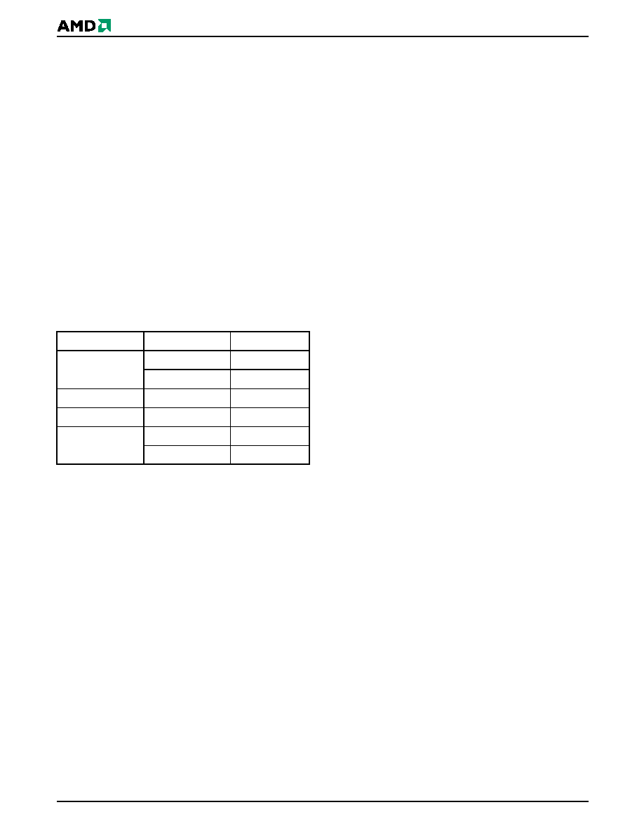
The device is divided as shown in the following table:
The device uses Chip Enable (CE#), Write Enable (WE#),
Address Valid (AVD#) and Output Enable (OE#) to control
asynchronous read and write operations. For burst opera-
tions, the device additionally requires Ready (RDY), and
Clock (CLK). This implementation allows easy interface with
minimal glue logic to a wide range of microprocessors/micro-
controllers for high performance read operations.
The burst read mode feature gives system designers flexibil-
ity in the interface to the device. The user can preset the
burst length and wrap through the same memory space, or
read the flash array in continuous mode.
The clock polarity feature provides system designers a
choice of active clock edges, either rising or falling. The ac-
tive clock edge initiates burst accesses and determines
when data will be output.
The device is entirely command set compatible with the
JEDEC 42.4 single-power-supply Flash standard. Com-
mands are written to the command register using standard
microprocessor write timing. Register contents serve as in-
puts to an internal state-machine that controls the erase and
programming circuitry. Write cycles also internally latch ad-
dresses and data needed for the programming and erase
operations. Reading data out of the device is similar to read-
ing from other Flash or EPROM devices.
The Erase Suspend/Erase Resume feature enables the
user to put erase on hold for any period of time to read data
from, or program data to, any sector that is not selected for
erasure. True background erase can thus be achieved.
The hardware RESET# pin terminates any operation in
progress and resets the internal state machine to reading
array data. The RESET# pin may be tied to the system reset
circuitry. A system reset would thus also reset the device,
enabling the system microprocessor to read boot-up firm-
ware from the Flash memory device.
The host system can detect whether a program or erase op-
eration is complete by using the device status bit DQ7
(Data# Polling) and DQ6/DQ2 (toggle bits). After a program
or erase cycle has been completed, the device automatically
returns to reading array data.
The sector erase architecture allows memory sectors to be
erased and reprogrammed without affecting the data con-
tents of other sectors. The device is fully erased when
shipped from the factory.
Hardware data protection measures include a low V
CC
de-
tector that automatically inhibits write operations during
power transitions. The device also offers two types of data
protection at the sector level. The sector lock/unlock com-
mand sequence disables or re-enables both program and
erase operations in any sector. When at V
IL
, WP# locks sec-
tors 0 and 1 (bottom boot device) or sectors 132 and 133
(top boot device).
The device offers two power-saving features. When ad-
dresses have been stable for a specified amount of time, the
device enters the automatic sleep mode. The system can
also place the device into the standby mode. Power con-
sumption is greatly reduced in both modes.
AMD's Flash technology combines years of Flash memory
manufacturing experience to produce the highest levels of
quality, reliability and cost effectiveness. The device electri-
cally erases all bits within a sector simultaneously via
Fowler-Nordheim tunnelling. The data is programmed using
hot electron injection.
Bank
Quantity
Size
A
4
8 Kwords
31
32 Kwords
B
32
32 Kwords
C
32
32 Kwords
D
31
32 Kwords
4
8 Kwords

November 1, 2002
Am42BDS640AG
3
P R E L I M I N A R Y
TABLE OF CONTENTS
Product Selector Guide . . . . . . . . . . . . . . . . . . . . . 5
MCP Block Diagram . . . . . . . . . . . . . . . . . . . . . . . . 5
Flash Memory Block Diagram. . . . . . . . . . . . . . . . 6
Flash Memory Simultaneous Operation Diagram 7
Connection Diagram . . . . . . . . . . . . . . . . . . . . . . . . 8
Special Package Handling Instructions .................................... 8
Pin Description . . . . . . . . . . . . . . . . . . . . . . . . . . . . 9
Logic Symbol . . . . . . . . . . . . . . . . . . . . . . . . . . . . . 9
Ordering Information . . . . . . . . . . . . . . . . . . . . . . 10
MCP Device Bus Operations. . . . . . . . . . . . . . . . 11
Table 1. Device Bus Operations ..................................................... 12
Flash Device Bus Operations . . . . . . . . . . . . . . . 13
Requirements for Asynchronous Read
Operation (Non-Burst) ............................................................ 13
Requirements for Synchronous (Burst) Read Operation ........ 13
8-, 16-, and 32-Word Linear Burst with Wrap Around ......... 13
Table 2. Burst Address Groups .......................................................13
Burst Mode Configuration Register ........................................ 14
Reduced Wait-State Handshaking Option .............................. 14
Simultaneous Read/Write Operations with Zero Latency ....... 14
Writing Commands/Command Sequences ............................ 14
Accelerated Program Operation .......................................... 14
Autoselect Functions ........................................................... 15
Standby Mode ........................................................................ 15
Automatic Sleep Mode ........................................................... 15
RESET#: Hardware Reset Input ............................................. 15
Output Disable Mode .............................................................. 15
Hardware Data Protection ...................................................... 15
Write Protect (WP#) ............................................................. 16
Low V
CC
Write Inhibit ........................................................... 16
Write Pulse "Glitch" Protection ............................................ 16
Logical Inhibit ...................................................................... 16
Power-Up Write Inhibit ......................................................... 16
Common Flash Memory Interface (CFI) . . . . . . . 16
Table 3. CFI Query Identification String ..........................................16
System Interface String................................................................... 17
Table 5. Device Geometry Definition .............................................. 17
Table 6. Primary Vendor-Specific Extended Query ........................18
Table 7. Sector Address Table ........................................................19
Flash Command Definitions . . . . . . . . . . . . . . . . 23
Reading Array Data ................................................................ 23
Set Burst Mode Configuration Register Command Sequence 23
Figure 1. Synchronous/Asynchronous State Diagram .................... 23
Read Mode Setting .............................................................. 23
Programmable Wait State Configuration ............................. 23
Table 8. Programmable Wait State Settings ...................................24
Handshaking Option ............................................................ 24
Table 9. Initial Access Codes ..........................................................24
Standard Handshaking Operation ....................................... 24
Table 10. Wait States for Standard Handshaking ...........................24
Burst Read Mode Configuration .......................................... 24
Table 11. Burst Read Mode Settings ..............................................25
Burst Active Clock Edge Configuration ................................ 25
RDY Configuration ............................................................... 25
Configuration Register ............................................................ 25
Table 12. Burst Mode Configuration Register .................................25
Sector Lock/Unlock Command Sequence .............................. 25
Reset Command ..................................................................... 25
Autoselect Command Sequence ............................................ 26
Table 13. Device IDs ...................................................................... 26
Program Command Sequence ............................................... 26
Unlock Bypass Command Sequence .................................. 27
Figure 2. Erase Operation.............................................................. 27
Chip Erase Command Sequence ........................................... 27
Sector Erase Command Sequence ........................................ 28
Erase Suspend/Erase Resume Commands ........................... 28
Figure 3. Program Operation ......................................................... 29
Command Definitions ............................................................. 30
Table 14. Command Definitions .................................................... 30
Flash Write Operation Status . . . . . . . . . . . . . . . 31
DQ7: Data# Polling ................................................................. 31
Figure 4. Data# Polling Algorithm .................................................. 31
RDY: Ready ............................................................................ 32
DQ6: Toggle Bit I .................................................................... 32
Figure 5. Toggle Bit Algorithm........................................................ 32
DQ2: Toggle Bit II ................................................................... 32
Table 15. DQ6 and DQ2 Indications .............................................. 33
Reading Toggle Bits DQ6/DQ2 ............................................... 33
DQ5: Exceeded Timing Limits ................................................ 33
DQ3: Sector Erase Timer ....................................................... 34
Table 16. Write Operation Status ................................................... 34
Absolute Maximum Ratings . . . . . . . . . . . . . . . . 35
Figure 6. Maximum Negative Overshoot Waveform ...................... 35
Figure 7. Maximum Positive Overshoot Waveform........................ 35
Operating Ranges . . . . . . . . . . . . . . . . . . . . . . . . . 35
Flash DC Characteristics . . . . . . . . . . . . . . . . . . 36
SRAM DC and Operating Characteristics . . . . . 37
Test Conditions . . . . . . . . . . . . . . . . . . . . . . . . . . 38
Figure 8. Test Setup....................................................................... 38
Table 17. Test Specifications ......................................................... 38
Key to Switching Waveforms. . . . . . . . . . . . . . . . 38
Figure 9. Input Waveforms and Measurement Levels ................... 38
AC Characteristics . . . . . . . . . . . . . . . . . . . . . . . . 39
SRAM CE#s Timing ................................................................ 39
Figure 10. Timing Diagram for Alternating
Between SRAM and Flash ............................................................. 39
Synchronous/Burst Read ........................................................ 40
Figure 11. CLK Synchronous Burst Mode Read
(rising active CLK).......................................................................... 41
Figure 12. CLK Synchronous Burst Mode Read
(Falling Active Clock) ..................................................................... 42
Figure 13. Synchronous Burst Mode Read .................................... 43
Figure 14. 8-word Linear Burst with Wrap Around ......................... 43
Figure 15. Burst with RDY Set One Cycle Before Data ................. 44
Figure 16. Reduced Wait-State Handshaking Burst Mode Read
Starting at an Even Address .......................................................... 45
Figure 17. Reduced Wait-State Handshaking Burst Mode Read
Starting at an Odd Address............................................................ 46
Asynchronous Read ............................................................... 47
Figure 18. Asynchronous Mode Read with Latched Addresses .... 47
Figure 19. Asynchronous Mode Read............................................ 48
Figure 20. Reset Timings ............................................................... 49
Erase/Program Operations ..................................................... 50
Figure 21. Asynchronous Program Operation Timings .................. 51
Figure 22. Alternate Asynchronous Program Operation Timings... 52
Figure 23. Synchronous Program Operation Timings.................... 53

4
Am42BDS640AG
November 1, 2002
P R E L I M I N A R Y
Figure 24. Alternate Synchronous Program Operation Timings ..... 54
Figure 25. Chip/Sector Erase Command Sequence ....................... 55
Figure 26. Accelerated Unlock Bypass Programming Timing......... 56
Figure 27. Data# Polling Timings (During Embedded Algorithm) ... 57
Figure 28. Toggle Bit Timings (During Embedded Algorithm)......... 57
Figure 29. Synchronous Data Polling Timings/Toggle Bit Timings . 58
Figure 30. Latency with Boundary Crossing ................................... 59
Figure 31. Latency with Boundary Crossing
into Program/Erase Bank ................................................................ 60
Figure 32. Example of Wait States Insertion (Standard
Handshaking Device) ...................................................................... 61
Figure 33. Back-to-Back Read/Write Cycle Timings ....................... 62
SRAM AC Characteristics . . . . . . . . . . . . . . . . . . 63
Read Cycle ............................................................................. 63
Figure 34. SRAM Read Cycle--Address Controlled....................... 63
Figure 35. SRAM Read Cycle ......................................................... 64
Write Cycle ............................................................................. 65
Figure 36. SRAM Write Cycle--WE# Control ................................ 65
Figure 37. SRAM Write Cycle--CE1#s Control ............................. 66
Figure 38. SRAM Write Cycle--UB#s and LB#s Control ............... 67
Flash Erase And Programming Performance . 68
Flash Latchup Characteristics. . . . . . . . . . . . . . . 68
Package Pin Capacitance . . . . . . . . . . . . . . . . . . 68
Flash Data Retention . . . . . . . . . . . . . . . . . . . . . . 68
SRAM Data Retention . . . . . . . . . . . . . . . . . . . . . 69
Figure 39. CE1#s Controlled Data Retention Mode....................... 69
Figure 40. CE2s Controlled Data Retention Mode......................... 69
Physical Dimensions . . . . . . . . . . . . . . . . . . . . . . 70
FSC093--93-Ball Fine-Pitch Grid Array 8 x 11.6 mm ............ 70
Revision Summary . . . . . . . . . . . . . . . . . . . . . . . . 71
Revision A (May 20, 2002) ..................................................... 71
Document Outline