
September 2003
This document specifies SPANSION
memory products that are now offered by both Advanced Micro Devices and
Fujitsu. Although the document is marked with the name of the company that originally developed the specification,
these products will be offered to customers of both AMD and Fujitsu.
Continuity of Specifications
There is no change to this datasheet as a result of offering the device as a SPANSION
product. Future routine
revisions will occur when appropriate, and changes will be noted in a revision summary.
Continuity of Ordering Part Numbers
AMD and Fujitsu continue to support existing part numbers beginning with "Am" and "MBM". To order these
products, please use only the Ordering Part Numbers listed in this document.
For More Information
Please contact your local AMD or Fujitsu sales office for additional information about SPANSION
memory
solutions.
TM
TM
TM
SPANSION MCP
Data Sheet
TM

DS05-50311-1E
FUJITSU SEMICONDUCTOR
DATA SHEET
Stacked MCP (Multi-Chip Package) FLASH MEMORY & FCRAM
CMOS
64 M (
◊
◊
◊
◊
16) FLASH MEMORY &
64 M (
◊
◊
◊
◊
16) Mobile FCRAM
TM
MB84VD23581FJ
-70
s
s
s
s
FEATURES
∑ Power Supply Voltage of 2.7 V to 3.1 V
∑ High Performance
70 ns maximum access time (Flash)
70 ns maximum access time (FCRAM)
∑ Operating Temperature
-
30
∞
C to
+
85
∞
C
∑ Package 65-ball FBGA
(Continued)
s
s
s
s
PRODUCT LINEUP
*: Both V
CC
f and V
CC
r must be the same level when either part is being accessed.
s
s
s
s
PACKAGE
Flash Memory
FCRAM
Power Supply Voltage ( V )
V
CC
f*
=
2.7 V to 3.1 V
V
CC
r*
=
2.7 V to 3.1 V
Max Address Access Time (ns)
70
70
Max CE Access Time (ns)
70
70
Max OE Access Time (ns)
30
40
65-ball plastic FBGA
(BGA-65P-M01)

MB84VD23581FJ
-70
2
(Continued)
1.
FLASH MEMORY
∑ 0.17
µ
µ
µ
µ
m Process Technology
∑ Simultaneous Read/Write Operations (Dual Bank)
∑ FlexBank
TM
*
1
Bank A : 8 Mbit (8 KB
◊
8 and 64 KB
◊
15)
Bank B : 24 Mbit (64 KB
◊
48)
Bank C : 24 Mbit (64 KB
◊
48)
Bank D : 8 Mbit (8 KB
◊
8 and 64 KB
◊
15)
Two virtual Banks are chosen from the combination of four physical banks
Host system can program or erase in one bank, and then read immediately and simultaneously from the other
bank with zero latency between read and write operations.
Read-while-erase
Read-while-program
∑ Single 3.0 V Read, Program, and Erase
Minimized system level power requirements
∑ Minimum 100,000 Program/Erase Cycles
∑ Sector Erase Architecture
Sixteen 4 Kword and one hundred twenty-six 32 Kword sectors in word.
Any combination of sectors can be concurrently erased. It also supports full chip erase.
∑ HiddenROM Region
256 byte of HiddenROM, accessible through a new "HiddenROM Enable" command sequence
Factory serialized and protected to provide a secure electronic serial number (ESN)
∑ WP/ACC Input Pin
At V
IL
, allows protection of "outermost" 2
◊
8 Kbytes on both ends of boot sectors, regardless of sector protection/
unprotection status
At V
IH
, allows removal of boot sector protection
At V
ACC
, increases program performance
∑ Embedded Erase
TM
*
2
Algorithms
Automatically preprograms and erases the chip or any sector
∑ Embedded Program
TM
*
2
Algorithms
Automatically writes and verifies data at specified address
∑ Data Polling and Toggle Bit Feature for Detection of Program or Erase Cycle Completion
∑ Ready/Busy Output (RY/BY)
Hardware method for detection of program or erase cycle completion
∑ Automatic Sleep Mode
When addresses remain stable, the device automatically switches itself to low power mode.
∑ Low V
CC
f Write Inhibit
2.5 V
∑ Program Suspend/Resume
Suspends the program operation to allow a read in another byte
∑ Erase Suspend/Resume
Suspends the erase operation to allow a read data and/or program in another sector within the same device
∑ Please Refer to "MBM29DL64DF" Datasheet in Detailed Function
(Continued)

MB84VD23581FJ
-70
3
(Continued)
2.
FCRAM
TM
*
3
∑ Power Dissipation
Operating : 25 mA Max
Standby : 200
µ
A Max
∑ Power Down Mode
Sleep : 10
µ
A Max
NAP : 65
µ
A Max
16M Partial : 85
µ
A Max
∑ Power Down Control by CE2r
∑ Byte Write Control: LB(DQ
7
to DQ
0
), UB(DQ
15
to DQ
8
)
∑ 8 words Address Access Capability
*1: FlexBank
TM
is a trademark of Fujitsu Limited, Japan.
*2: Embedded Erase
TM
and Embedded Program
TM
are trademarks of Advanced Micro Devices, Inc.
*3: FCRAM
TM
is a trademark of Fujitsu Limited, Japan.

MB84VD23581FJ
-70
4
s
s
s
s
PIN ASSIGNMENT
FBGA
(TOP VIEW)
Marking side
(BGA-65P-M01)
D8
A
13
D7
A
9
D6
A
20
D5
RY/BY
D4
A
18
D3
A
5
D2
A
2
D9
A21
F8
F7
DQ
6
DQ
1
F3
V
SS
F2
A
0
F9
A
16
G8
DQ
15
G7
DQ
13
G6
DQ
4
G5
DQ
3
G4
DQ
9
G3
OE
G2
CEf
G9
E8
A
14
E7
A
10
E4
A
17
E3
A
4
E2
A
1
E9
PE
H8
DQ
7
H7
DQ
12
H6
Vccr
H5
Vccf
Vccf
H4
DQ
10
H3
DQ
0
H2
CE1r
H9
Vss
J8
DQ
14
J7
DQ
5
J6
J5
DQ
11
J4
DQ
2
J3
DQ
8
K9
N.C.
N.C.
N.C.
K2
N.C.
K1
N.C.
K10
N.C.
C8
A
12
C7
A
19
C6
CE2r
C5
RESET
C4
UB
C3
A
6
C2
A
3
C9
A
15
B8
A
11
B7
A
8
B6
WE
B5
WP/ACC
B4
LB
B3
A
7
A9
N.C.
B1
N.C.
A10
N.C.
A2
N.C.
A1
N.C.
F4
MB84VD23581FJ
-70
5
s
s
s
s
PIN DESCRIPTION
s
s
s
s
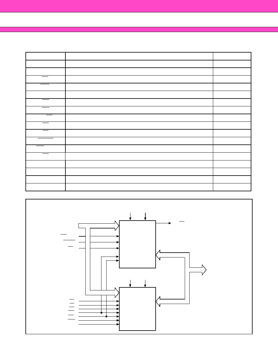
BLOCK DIAGRAM
Pin Name
Function
Input/Output
A
21
to A
0
Address Inputs (Common)
I
DQ
15
to DQ
0
Data Inputs/Outputs (Common)
I/O
CEf
Chip Enable (Flash)
I
CE1r
Chip Enable (FCRAM)
I
CE2r
Chip Enable (FCRAM)
I
OE
Output Enable (Common)
I
WE
Write
Enable
(Common) I
RY/BY
Ready/Busy Outputs (Flash) Open Drain Output
O
UB
Upper Byte Control (FCRAM)
I
LB
Lower Byte Control (FCRAM)
I
RESET
Hardware Reset Pin/Sector Protection Unlock (Flash)
I
WP/ACC
Write Protect/Acceleration (Flash)
I
PE
Partial Enable (FCRAM)
I
N.C.
No Internal Connection
V
SS
Device Ground (Common)
Power
V
CC
f
Device Power Supply (Flash)
Power
V
CC
r
Device Power Supply (FCRAM)
Power
V
SS
V
CC
r
64 M bit
RESET
Flash Memory
WE
64 M bit
FCRAM
CEf
A
21
to A
0
OE
CE1r
V
SS
V
CC
f
A
21
to A
0
A
21
to A
0
DQ
15
to DQ
0
RY/BY
LB
UB
WP/ACC
CE2r
DQ
15
to DQ
0
DQ
15
to DQ
0
PE

MB84VD23581FJ
-70
6
s
s
s
s
DEVICE BUS OPERATIONS
Legend: L = V
IL
, H = V
IH
, X = V
IL
or V
IH
. See DC Characteristics for voltage levels.
*1 : Other operations except for indicated this column are prohibited.
*2 : Do not apply CEf = V
IL
, CE1r = V
IL
and CE2r = V
IH
all at once.
*3 : FCRAM Output Disable condition should not be kept longer than 1
µ
s.
*4 : WE can be V
IL
if OE is V
IL
, OE at V
IH
initiates the write operations.
*5 : FCRAM LB,UB control at Read operation is not supported.
*6 : It is also used for the extended sector group protections.
*7 : The FCRAM Power Down Program can be performed one time after compliance of Power-UP timings and it
should not be re-programmed after regular Read or Write.
*8 : FCRAM Power Down mode can be entered from Standby state and all DQ pins are in High-Z state.
I
PD
r current and data retention depends on the selection of Power Down Program.
*9 : Either or both LB and UB must be Low for FCRAM Read Operation.
*10 : Can be either V
IL
or V
IH
but must be valid before Read or Write.
*11 : See " FCRAM Power Down Program Key Table " in next page.
*12 : Protect " outer most " 2
◊
8K bytes ( 4 words ) on both ends of the boot block sectors.
Operation *
1,
*
2
CEf
CE1r CE2r
OE WE
LB
UB
PE
A
21
to A
0
DQ
7
to
DQ
0
DQ
15
to
DQ
8
RESET
WP/
ACC*
12
Full Standby
H
H
H
X
X
X
X
H
X
High-Z
High-Z
H
X
Output Disable *
3
H
L
H
H
H
X
X
H
X *
10
High-Z
High-Z
H
X
L
H
H
H
H
X
X
H
X
High-Z
High-Z
H
X
Read from Flash *
4
L
H
H
L
H
X
X
H
Vaild
D
OUT
D
OUT
H
X
Write to Flash
L
H
H
H
L
X
X
H
Vaild
D
IN
D
IN
H
X
Read from FCRAM *
5
H
L
H
L
H
L *
9
L *
9
H
Vaild
D
OUT
D
OUT
H
X
Write to FCRAM
H
L
H
H
L
L
L
H
Vaild
D
IN
D
IN
H
X
H
L
High-Z
D
IN
L
H
D
IN
High-Z
Temporary Sector
Group Unprotection
*
6
X
X
X
X
X
X
X
X
X
X
X
V
ID
X
Flash Hardware
Reset
X
H
H
X
X
X
X
X
X
High-Z
High-Z
L
X
Boot Block Sector
Write Protection
X
X
X
X
X
X
X
X
X
X
X
X
L
FCRAM Power Down
Program *
7
H
H
H
X
X
X
X
L
Vaild
High-Z
High-Z
H
X
FCRAM No Read
H
L
H
L
H
H
H
H
Vaild
High-Z
High-Z
H
X
FCRAM Power Down
*
8
X
X
L
X
X
X
X
X
X
X
X
X
X
MB84VD23581FJ
-70
7
s
s
s
s
ABSOLUTE MAXIMUM RATINGS
*1: Minimum DC voltage on input or I/O pins is ≠0.3 V. During voltage transitions, input or I/O pins may undershoot
V
SS
to ≠1.0 V for periods of up to 20 ns. Maximum DC voltage on input or I/O pins is V
CC
f+0.3 V or V
CC
r+0.3 V.
During voltage transitions, input or I/O pins may overshoot to V
CC
f+1.0 V or V
CC
r+1.0 V for periods of up to 5 ns.
*2: Minimum DC input voltage on RESET pin is ≠0.5 V. During voltage transitions, RESET pin may undershoot V
SS
to ≠2.0 V for periods of up to 20 ns.
Voltage difference between input and supply voltage (V
IN
-V
CC
f or V
CC
r) does not exceed 9.0 V.
Maximum DC input voltage on RESET pin is +13.0 V which may overshoot to +14.0 V for periods of up to 20 ns.
*3: Minimum DC input voltage on WP/ACC pin is ≠0.5 V. During voltage transitions, WP/ACC pin may undershoot
Vss to ≠2.0 V for periods of up to 20 ns. Maximum DC input voltage on WP/ACC pin is +10.5 V which may
overshoot to +10.5 V for periods of up to 20 ns, when V
CC
f is applied.
WARNING: Semiconductor devices can be permanently damaged by application of stress (voltage, current,
temperature, etc.) in excess of absolute maximum ratings. Do not exceed these ratings.
s
s
s
s
RECOMMENDED OPERATING CONDITIONS
WARNING: The recommended operating conditions are required in order to ensure the normal operation of the
semiconductor device. All of the device's electrical characteristics are warranted when the device is
operated within these ranges.
Always use semiconductor devices within their recommended operating condition ranges. Operation
outside these ranges may adversely affect reliability and could result in device failure.
No warranty is made with respect to uses, operating conditions, or combinations not represented on
the data sheet. Users considering application outside the listed conditions are advised to contact their
FUJITSU representatives beforehand.
Parameter
Symbol
Rating
Unit
Min
Max
Storage Temperature
Tstg
-
55
+
125
∞
C
Ambient Temperature with Power Applied
T
A
-
30
+
85
∞
C
Voltage with Respect to Ground All pins *
1
V
IN
-
0.3
V
CC
f
+
0.3
V
V
OUT
-
0.3
V
CC
r
+
0.3
V
V
CC
f Supply *
1
V
CC
f
-
0.2
+
3.6
V
V
CC
r Supply *
1
V
CC
r
-
0.2
+
3.6
V
RESET *
2
V
IN
-
0.5
+
13.0
V
WP/ACC *
3
V
IN
-
0.5
+
10.5
V
Parameter
Symbol
Value
Unit
Min
Max
Ambient Temperature
T
A
-
30
+
85
∞
C
V
CC
f Supply Voltages
V
CC
f
+
2.7
+
3.1
V
V
CC
r Supply Voltages
V
CC
r
+
2.7
+
3.1
V
MB84VD23581FJ
-70
8
s
s
s
s
ELECTRICAL CHARACTERISTICS
1.
DC Characteristics *
1,
*
2,
*
3
(Continued)
Parameter
Symbol
Test Conditions
Value
Unit
Min
Typ
Max
Input Leakage Current
I
LI
V
IN
= V
SS
to V
CC
f, V
CC
r
≠1.0
--
+1.0
µ
A
Output Leakage Current
I
LO
V
OUT
= V
SS
to V
CC
f, V
CC
r
≠1.0
--
+1.0
µ
A
RESET Inputs Leakage
Current
I
LIT
V
CC
f
= V
CC
f Max,
RESET = 12.5 V
--
--
35
µA
Flash V
CC
Active Current
(Read) *
4
I
CC1
f
CEf = V
IL
, OE = V
IH
t
CYCLE
= 5 MHz
--
--
18
mA
t
CYCLE
= 1 MHz
--
--
4
mA
Flash V
CC
Active Current
(Program/Erase) *
5
I
CC2
f
CEf = V
IL
, OE = V
IH
--
--
35
mA
Flash V
CC
Active Current
(Read-While-Program) *
6
I
CC3
f
CEf = V
IL
, OE = V
IH
--
--
53
mA
Flash V
CC
Active Current
(Read-While-Erase) *
8
I
CC4
f
CEf = V
IL
, OE = V
IH
--
--
53
mA
Flash V
CC
Active Current *
8
(Erase-Suspend-Program)
I
CC5
f
CEf = V
IL
, OE = V
IH
--
--
40
mA
WP/ACC Acceleration
Program Current
I
ACC
V
CC
f = V
CC
f Max,
WP/ACC = V
ACC
Max
--
--
20
mA
FCRAM V
CC
Active Current
I
CC1
r
V
CC
r = V
CC
r Max,
CE1r = V
IL
, CE2r = V
IH
,
V
IN
= V
IH
or V
IL
,
I
OUT
= 0 mA
t
RC
/ t
WC
= Min
--
--
25
mA
t
RC
/ t
WC
= 1
µ
s
--
--
3
Flash V
CC
Standby Current
I
SB1
f
V
CC
f = V
CC
f Max, CEf = V
CC
f ± 0.3 V,
RESET = V
CC
f ± 0.3 V,
WP/ACC = V
CC
f± 0.3 V
--
1
5
µ
A
Flash V
CC
Standby Current
(RESET)
I
SB2
f
V
CC
f = V
CC
f Max, RESET = V
SS
± 0.3 V,
WP/ACC = V
CC
f± 0.3 V
--
1
5
µ
A
Flash V
CC
Current
(Automatic Sleep Mode) *
6
I
SB3
f
V
CC
f = V
CC
f Max, CEf = V
SS
± 0.3 V
RESET = V
CC
f ± 0.3 V,
WP/ACC = V
CC
f± 0.3 V,
V
IN
= V
CC
f± 0.3 V or V
SS
± 0.3 V
--
1
5
µ
A
FCRAM V
CC
Standby
Current
I
SB1
r
V
CC
r = V
CC
r Max,CE1r > V
CC
r ≠ 0.2 V,
CE2r > V
CC
r≠ 0.2 V,
V
IN
< 0.2 V or V
CC
r ≠ 0.2 V
--
--
200
µ
A
FCRAM V
CC
Power Down
Current
I
PDS
r
V
CC
r = V
CC
r Max,
CE1r > V
CC
r ≠ 0.2V,
CE2r < 0.2V
Sleep
--
--
10
µ
A
I
PDN
r
NAP
--
--
65
µ
A
I
PD8
r
16M
Partial
--
--
85
µ
A
MB84VD23581FJ
-70
9
(Continued)
*1 : All voltage are referenced to V
SS
.
*2 : FCRAM DC characteristics are measured after following POWER-UP timing.
*3 : I
OUT
depends on the output load conditions.
*4 : The I
CC
current listed includes both the DC operating current and the frequency dependent component.
*5 : I
CC
active while Embedded Algorithm (program or erase) is in progress.
*6 : Automatic sleep mode enables the low power mode when address remain stable for 150 ns.
*7 : Applicable for only V
CC
applying.
*8 : Embedded Algorithm (program or erase) is in progress. (@5 MHz)
Parameter
Symbol
Test Conditions
Value
Unit
Min
Typ
Max
Input Low Level
V
IL
--
≠0.3
--
0.5
V
Input High Level
V
IH
--
Flash
2.0
--
V
CC
f+0.3
V
FCRAM
2.2
V
CC
r+0.3
Voltage for Autoselect and
Sector Protection (RESET) *
7
V
ID
--
11.5
--
12.5
V
Voltage for WP/ACC Sector
Protection/Unprotection and
Program Acceleration
V
ACC
--
8.5
9.0
9.5
V
FCRAM Output Low Level
V
OL
V
CC
r = V
CC
r Min, I
OL
=1.0 mA
--
--
0.4
V
FCRAM Output High Level
V
OH
V
CC
r = V
CC
r Min, I
OH
= ≠0.5 mA
2.2
--
--
V
Flash Output Low Level
V
OL
V
CC
f = V
CC
f Min, I
OL
= 4.0 mA
--
--
0.45
V
Flash Output High Level
V
OH
V
CC
f = V
CC
f Min, I
OH
= ≠0.1 mA
V
CC
f≠0.4
--
--
V
Flash Low V
CC
Lock-Out
Voltage
V
LKO
--
2.3
2.4
2.5
V
MB84VD23581FJ
-70
10
2.
AC Characteristics
∑
CE Timing
∑
Timing Diagram for alternating FCRAM to Flash
Parameter
Symbol
Condition
Value
Unit
JEDEC
Standard
Min
CE Recover Time
t
CCR
0
ns
CE Hold Time
t
CHOLD
3
ns
CE1r High to WE Invalid time for
Standby Entry
--
t
CHWX
--
10
ns
CEf
t
CCR
t
CCR
CE1r
CE2r
t
CCR
t
CCR
WE
t
CHWX
t
CHOLD
MB84VD23581FJ
-70
11
s
s
s
s
64 M FLASH MEMORY CHARACTERISTICS for MCP
1.
Flexible Sector-Erase Architecture on Flash Memory
∑ Sixteen 4K words, and one hundred twenty-six 32 K words.
∑ Individual-sector, multiple-sector, or bulk-erase capability.
Sector Architecture
SA31 : 64KB (32KW)
SA30 : 64KB (32KW)
SA29 : 64KB (32KW)
SA28 : 64KB (32KW)
SA27 : 64KB (32KW)
SA26 : 64KB (32KW)
SA25 : 64KB (32KW)
SA24 : 64KB (32KW)
SA23 : 64KB (32KW)
SA22 : 64KB (32KW)
SA21 : 64KB (32KW)
SA20 : 64KB (32KW)
SA19 : 64KB (32KW)
SA18 : 64KB (32KW)
SA17 : 64KB (32KW)
SA16 : 64KB (32KW)
SA15 : 64KB (32KW)
SA14 : 64KB (32KW)
SA13 : 64KB (32KW)
SA12 : 64KB (32KW)
SA11 : 64KB (32KW)
SA10 : 64KB (32KW)
SA9 : 64KB (32KW)
SA8 : 64KB (32KW)
SA7 : 8KB (4KW)
SA6 : 8KB (4KW)
SA5 : 8KB (4KW)
SA4 : 8KB (4KW)
SA3 : 8KB (4KW)
SA2 : 8KB (4KW)
SA70 : 64KB (32KW)
SA69 : 64KB (32KW)
SA68 : 64KB (32KW)
SA67 : 64KB (32KW)
SA66 : 64KB (32KW)
SA65 : 64KB (32KW)
SA64 : 64KB (32KW)
SA63 : 64KB (32KW)
SA62 : 64KB (32KW)
SA61 : 64KB (32KW)
SA60 : 64KB (32KW)
SA59 : 64KB (32KW)
SA58 : 64KB (32KW)
SA57 : 64KB (32KW)
SA56 : 64KB (32KW)
SA55 : 64KB (32KW)
SA54 : 64KB (32KW)
SA53 : 64KB (32KW)
SA52 : 64KB (32KW)
SA51 : 64KB (32KW)
SA50 : 64KB (32KW)
SA49 : 64KB (32KW)
SA48 : 64KB (32KW)
SA47 : 64KB (32KW)
SA46 : 64KB (32KW)
SA45 : 64KB (32KW)
SA44 : 64KB (32KW)
SA43 : 64KB (32KW)
SA42 : 64KB (32KW)
SA41 : 64KB (32KW)
SA40 : 64KB (32KW)
SA39 : 64KB (32KW)
SA38 : 64KB (32KW)
SA37 : 64KB (32KW)
SA36 : 64KB (32KW)
SA35 : 64KB (32KW)
SA34 : 64KB (32KW)
SA33 : 64KB (32KW)
SA32 : 64KB (32KW)
SA1 : 8KB (4KW)
SA0 : 8KB (4KW)
Bank A
Bank B
070000h
078000h
060000h
068000h
050000h
058000h
040000h
048000h
030000h
038000h
020000h
028000h
010000h
018000h
007000h
008000h
005000h
006000h
003000h
004000h
001000h
002000h
000000h
SA102 : 64KB (32KW)
SA101 : 64KB (32KW)
SA100 : 64KB (32KW)
SA99 : 64KB (32KW)
SA98 : 64KB (32KW)
SA97 : 64KB (32KW)
SA96 : 64KB (32KW)
SA95 : 64KB (32KW)
SA94 : 64KB (32KW)
SA93 : 64KB (32KW)
SA92 : 64KB (32KW)
SA91 : 64KB (32KW)
SA90 : 64KB (32KW)
SA89 : 64KB (32KW)
SA88 : 64KB (32KW)
SA87 : 64KB (32KW)
SA86 : 64KB (32KW)
SA85 : 64KB (32KW)
SA84 : 64KB (32KW)
SA83 : 64KB (32KW)
SA82 : 64KB (32KW)
SA81 : 64KB (32KW)
SA80 : 64KB (32KW)
SA79 : 64KB (32KW)
SA78 : 64KB (32KW)
SA77 : 64KB (32KW)
SA76 : 64KB (32KW)
SA75 : 64KB (32KW)
SA74 : 64KB (32KW)
SA73 : 64KB (32KW)
3FFFFFh
SA141 : 8KB (4KW)
SA140 : 8KB (4KW)
SA139 : 8KB (4KW)
SA138 : 8KB (4KW)
SA137 : 8KB (4KW)
SA136 : 8KB (4KW)
SA135 : 8KB (4KW)
SA134 : 8KB (4KW)
SA133 : 64KB (32KW)
SA132 : 64KB (32KW)
SA131 : 64KB (32KW)
SA130 : 64KB (32KW)
SA129 : 64KB (32KW)
SA128 : 64KB (32KW)
SA127 : 64KB (32KW)
SA126 : 64KB (32KW)
SA125 : 64KB (32KW)
SA124 : 64KB (32KW)
SA123 : 64KB (32KW)
SA122 : 64KB (32KW)
SA121 : 64KB (32KW)
SA120 : 64KB (32KW)
SA119 : 64KB (32KW)
SA118 : 64KB (32KW)
SA117 : 64KB (32KW)
SA116 : 64KB (32KW)
SA115 : 64KB (32KW)
SA114 : 64KB (32KW)
SA113 : 64KB (32KW)
SA112 : 64KB (32KW)
SA111 : 64KB (32KW)
SA110 : 64KB (32KW)
SA109 : 64KB (32KW)
SA108 : 64KB (32KW)
SA107 : 64KB (32KW)
SA106 : 64KB (32KW)
SA105 : 64KB (32KW)
SA104 : 64KB (32KW)
SA103 : 64KB (32KW)
SA72 : 64KB (32KW)
SA71 : 64KB (32KW)
Bank C
Bank D
3FF000h
3FE000h
3FD000h
3FC000h
3FB000h
3FA000h
3F9000h
0F0000h
0F8000h
0E0000h
0E8000h
0D0000h
0D8000h
0C0000h
0C8000h
0B0000h
0B8000h
0A0000h
0A8000h
090000h
098000h
088000h
080000h
170000h
178000h
160000h
168000h
150000h
158000h
140000h
148000h
130000h
138000h
120000h
128000h
110000h
118000h
100000h
108000h
1F0000h
1F8000h
1E0000h
1E8000h
1D0000h
1D8000h
1C0000h
1C8000h
1B0000h
1B8000h
1A0000h
1A8000h
190000h
198000h
188000h
180000h
270000h
278000h
260000h
268000h
250000h
258000h
240000h
248000h
230000h
238000h
220000h
228000h
210000h
218000h
208000h
2F0000h
2F8000h
2E0000h
2E8000h
2D0000h
2D8000h
2C0000h
2C8000h
2B0000h
2B8000h
2A0000h
2A8000h
290000h
298000h
288000h
280000h
370000h
378000h
360000h
368000h
350000h
358000h
340000h
348000h
330000h
338000h
320000h
328000h
310000h
318000h
300000h
308000h
3F0000h
3F8000h
3E0000h
3E8000h
3D0000h
3D8000h
3C0000h
3C8000h
3B0000h
3B8000h
3A0000h
3A8000h
390000h
398000h
388000h
380000h
200000h
1FFFFFh
Word Mode
Word Mode
MB84VD23581FJ
-70
12
FlexBank
TM
Architecture
Example of Virtual Banks Combination
Note : When multiple sector erase over several banks is operated, the system cannot read out of the bank to which
a sector being erased belongs. For example, suppose that erasing is taking place at both Bank A and Bank B,
neither Bank A nor Bank B is read out (they would output the sequence flag once they were selected.)
Meanwhile the system would get to read from either Bank C or Bank D.
Simultaneous Operation
* : By writing erase suspend command on the bank address of sector being erased, the erase operation gets
suspended so that it enables reading from or programming the remaining sectors.
Note: Bank 1 and Bank 2 are divided for the sake of convenience at Simultaneous Operation. Actually, the
Bank consists of 4 banks, Bank A, Bank B, BankC and Bank D. Bank Address (BA) meant to specify each
of the Banks.
Bank
Splits
Bank 1
Bank 2
Volume
Combination
Volume
Combination
1
8 Mbit
Bank A
56 Mbit
Remainder (Bank B, C, D)
2
24 Mbit
Bank B
40 Mbit
Remainder (Bank A, C, D)
3
24 Mbit
Bank C
40 Mbit
Remainder (Bank A, B, D)
4
8 Mbit
Bank D
56 Mbit
Remainder (Bank A, B, C)
Bank
Splits
Bank 1
Bank 2
Volume Combination
Sector Size
Volume Combination
Sector Size
1
8 Mbit
Bank A
8
◊
8 Kbyte/4 Kword
+
15
◊
64 Kbyte/32 Kword
56 Mbit
Bank B
+
Bank C
+
Bank D
8
◊
8 Kbyte/4 Kword
+
111
◊
64 Kbyte/32 Kword
2
16 Mbit
Bank A
+
Bank D
16
◊
8 Kbyte/4 Kword
+
30
◊
64 Kbyte/32 Kword
48 Mbit
Bank B
+
Bank C
96
◊
64 Kbyte/32 Kword
3
24 Mbit
Bank B
48
◊
64 Kbyte/32 Kword 40 Mbit
Bank A
+
Bank C
+
Bank D
16
◊
8 Kbyte/4 Kword
+
78
◊
64 Kbyte/32 Kword
4
32 Mbit
Bank A
+
Bank B
8
◊
8 Kbyte/4 Kword
+
63
◊
64 Kbyte/32 Kword
32 Mbit
Bank C
+
Bank D
8
◊
8 Kbyte/4 Kword
+
63
◊
64 Kbyte/32 Kword
Case
Bank 1 Status
Bank 2 Status
1
Read mode
Read mode
2
Read mode
Autoselect mode
3
Read mode
Program mode
4
Read mode
Erase mode *
5
Autoselect mode
Read mode
6
Program mode
Read mode
7
Erase mode *
Read mode
MB84VD23581FJ
-70
13
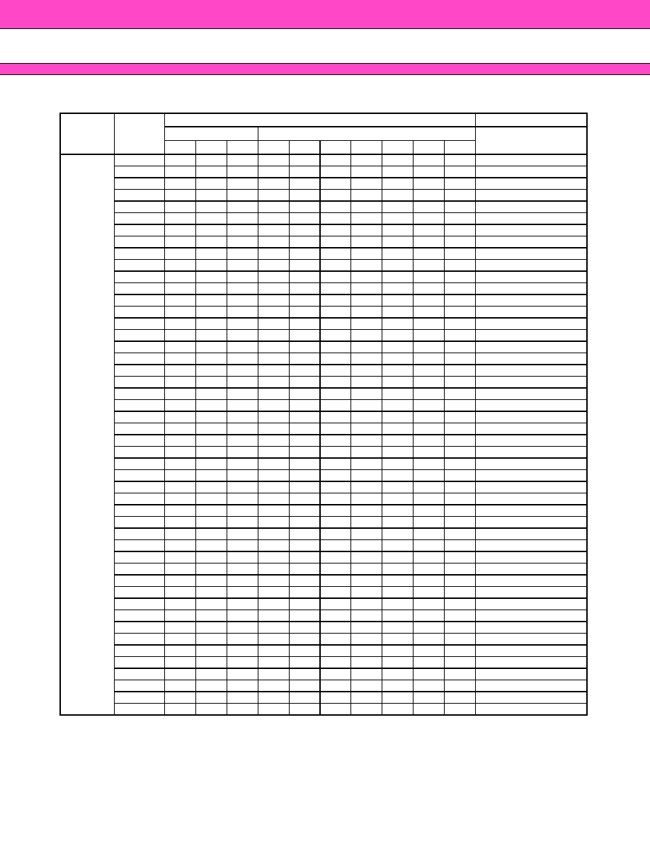
Sector Address Tables
(Continued)
Bank
Sector
Sector Address
Address Range
Bank Address
Word Mode
A
21
A
20
A
19
A
18
A
17
A
16
A
15
A
14
A
13
A
12
Bank A
SA0
0
0
0
0
0
0
0
0
0
0
000000h to 000FFFh
SA1
0
0
0
0
0
0
0
0
0
1
001000h to 001FFFh
SA2
0
0
0
0
0
0
0
0
1
0
002000h to 002FFFh
SA3
0
0
0
0
0
0
0
0
1
1
003000h to 003FFFh
SA4
0
0
0
0
0
0
0
1
0
0
004000h to 004FFFh
SA5
0
0
0
0
0
0
0
1
0
1
005000h to 005FFFh
SA6
0
0
0
0
0
0
0
1
1
0
006000h to 006FFFh
SA7
0
0
0
0
0
0
0
1
1
1
007000h to 007FFFh
SA8
0
0
0
0
0
0
1
X
X
X
008000h to 00FFFFh
SA9
0
0
0
0
0
1
0
X
X
X
010000h to 017FFFh
SA10
0
0
0
0
0
1
1
X
X
X
018000h to 01FFFFh
SA11
0
0
0
0
1
0
0
X
X
X
020000h to 027FFFh
SA12
0
0
0
0
1
0
1
X
X
X
028000h to 02FFFFh
SA13
0
0
0
0
1
1
0
X
X
X
030000h to 037FFFh
SA14
0
0
0
0
1
1
1
X
X
X
038000h to 03FFFFh
SA15
0
0
0
1
0
0
0
X
X
X
040000h to 047FFFh
SA16
0
0
0
1
0
0
1
X
X
X
048000h to 04FFFFh
SA17
0
0
0
1
0
1
0
X
X
X
050000h to 057FFFh
SA18
0
0
0
1
0
1
1
X
X
X
058000h to 05FFFFh
SA19
0
0
0
1
1
0
0
X
X
X
060000h to 067FFFh
SA20
0
0
0
1
1
0
1
X
X
X
068000h to 06FFFFh
SA21
0
0
0
1
1
1
0
X
X
X
070000h to 077FFFh
SA22
0
0
0
1
1
1
1
X
X
X
078000h to 07FFFFh

MB84VD23581FJ
-70
14
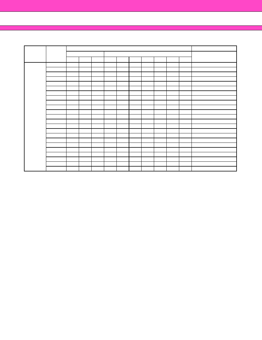
(Continued)
(Continued)
Bank
Sector
Sector Address
Address Range
Bank Address
Word Mode
A
21
A
20
A
19
A
18
A
17
A
16
A
15
A
14
A
13
A
12
Bank B
SA23
0
0
1
0
0
0
0
X
X
X
080000h to 087FFFh
SA24
0
0
1
0
0
0
1
X
X
X
088000h to 08FFFFh
SA25
0
0
1
0
0
1
0
X
X
X
090000h to 097FFFh
SA26
0
0
1
0
0
1
1
X
X
X
098000h to 09FFFFh
SA27
0
0
1
0
1
0
0
X
X
X
0A0000h to 0A7FFFh
SA28
0
0
1
0
1
0
1
X
X
X
0A8000h to 0AFFFFh
SA29
0
0
1
0
1
1
0
X
X
X
0B0000h to 0B7FFFh
SA30
0
0
1
0
1
1
1
X
X
X
0B8000h to 0BFFFFh
SA31
0
0
1
1
0
0
0
X
X
X
0C0000h to 0C7FFFh
SA32
0
0
1
1
0
0
1
X
X
X
0C8000h to 0CFFFFh
SA33
0
0
1
1
0
1
0
X
X
X
0D0000h to 0D7FFFh
SA34
0
0
1
1
0
1
1
X
X
X
0D8000h to 0DFFFFh
SA35
0
0
1
1
1
0
0
X
X
X
0E0000h to 0E7FFFh
SA36
0
0
1
1
1
0
1
X
X
X
0E8000h to 0EFFFFh
SA37
0
0
1
1
1
1
0
X
X
X
0F0000h to 0F7FFFh
SA38
0
0
1
1
1
1
1
X
X
X
0F8000h to 0FFFFFh
SA39
0
1
0
0
0
0
0
X
X
X
100000h to 107FFFh
SA40
0
1
0
0
0
0
1
X
X
X
108000h to 10FFFFh
SA41
0
1
0
0
0
1
0
X
X
X
110000h to 117FFFh
SA42
0
1
0
0
0
1
1
X
X
X
118000h to 11FFFFh
SA43
0
1
0
0
1
0
0
X
X
X
120000h to 127FFFh
SA44
0
1
0
0
1
0
1
X
X
X
128000h to 12FFFFh
SA45
0
1
0
0
1
1
0
X
X
X
130000h to 137FFFh
SA46
0
1
0
0
1
1
1
X
X
X
138000h to 13FFFFh
SA47
0
1
0
1
0
0
0
X
X
X
140000h to 147FFFh
SA48
0
1
0
1
0
0
1
X
X
X
148000h to 14FFFFh
SA49
0
1
0
1
0
1
0
X
X
X
150000h to 157FFFh
SA50
0
1
0
1
0
1
1
X
X
X
158000h to 15FFFFh
SA51
0
1
0
1
1
0
0
X
X
X
160000h to 167FFFh
SA52
0
1
0
1
1
0
1
X
X
X
168000h to 16FFFFh
SA53
0
1
0
1
1
1
0
X
X
X
170000h to 177FFFh
SA54
0
1
0
1
1
1
1
X
X
X
178000h to 17FFFFh
SA55
0
1
1
0
0
0
0
X
X
X
180000h to 187FFFh
SA56
0
1
1
0
0
0
1
X
X
X
188000h to 18FFFFh
SA57
0
1
1
0
0
1
0
X
X
X
190000h to 197FFFh
SA58
0
1
1
0
0
1
1
X
X
X
198000h to 19FFFFh
SA59
0
1
1
0
1
0
0
X
X
X
1A0000h to 1A7FFFh
SA60
0
1
1
0
1
0
1
X
X
X
1A8000h to 1AFFFFh
SA61
0
1
1
0
1
1
0
X
X
X
1B0000h to 1B7FFFh
SA62
0
1
1
0
1
1
1
X
X
X
1B8000h to 1BFFFFh
SA63
0
1
1
1
0
0
0
X
X
X
1C0000h to 1C7FFFh
SA64
0
1
1
1
0
0
1
X
X
X
1C8000h to 1CFFFFh
SA65
0
1
1
1
0
1
0
X
X
X
1D0000h to 1D7FFFh
SA66
0
1
1
1
0
1
1
X
X
X
1D8000h to 1DFFFFh
SA67
0
1
1
1
1
0
0
X
X
X
1E0000h to 1E7FFFh
SA68
0
1
1
1
1
0
1
X
X
X
1E8000h to 1EFFFFh
SA69
0
1
1
1
1
1
0
X
X
X
1F0000h to 1F7FFFh
SA70
0
1
1
1
1
1
1
X
X
X
1F8000h to 1FFFFFh
MB84VD23581FJ
-70
15
(Continued)
(Continued)
Bank
Sector
Sector Address
Address Range
Bank Address
Word Mode
A
21
A
20
A
19
A
18
A
17
A
16
A
15
A
14
A
13
A
12
Bank C
SA71
1
0
0
0
0
0
0
X
X
X
200000h to 207FFFh
SA72
1
0
0
0
0
0
1
X
X
X
208000h to 20FFFFh
SA73
1
0
0
0
0
1
0
X
X
X
210000h to 217FFFh
SA74
1
0
0
0
0
1
1
X
X
X
218000h to 21FFFFh
SA75
1
0
0
0
1
0
0
X
X
X
220000h to 227FFFh
SA76
1
0
0
0
1
0
1
X
X
X
228000h to 22FFFFh
SA77
1
0
0
0
1
1
0
X
X
X
230000h to 237FFFh
SA78
1
0
0
0
1
1
1
X
X
X
238000h to 23FFFFh
SA79
1
0
0
1
0
0
0
X
X
X
240000h to 247FFFh
SA80
1
0
0
1
0
0
1
X
X
X
248000h to 24FFFFh
SA81
1
0
0
1
0
1
0
X
X
X
250000h to 257FFFh
SA82
1
0
0
1
0
1
1
X
X
X
258000h to 25FFFFh
SA83
1
0
0
1
1
0
0
X
X
X
260000h to 267FFFh
SA84
1
0
0
1
1
0
1
X
X
X
268000h to 26FFFFh
SA85
1
0
0
1
1
1
0
X
X
X
270000h to 277FFFh
SA86
1
0
0
1
1
1
1
X
X
X
278000h to 27FFFFh
SA87
1
0
1
0
0
0
0
X
X
X
280000h to 287FFFh
SA88
1
0
1
0
0
0
1
X
X
X
288000h to 28FFFFh
SA89
1
0
1
0
0
1
0
X
X
X
290000h to 297FFFh
SA90
1
0
1
0
0
1
1
X
X
X
298000h to 29FFFFh
SA91
1
0
1
0
1
0
0
X
X
X
2A0000h to 2A7FFFh
SA92
1
0
1
0
1
0
1
X
X
X
2A8000h to 2AFFFFh
SA93
1
0
1
0
1
1
0
X
X
X
2B0000h to 2B7FFFh
SA94
1
0
1
0
1
1
1
X
X
X
2B8000h to 2BFFFFh
SA95
1
0
1
1
0
0
0
X
X
X
2C0000h to 2C7FFFh
SA96
1
0
1
1
0
0
1
X
X
X
2C8000h to 2CFFFFh
SA97
1
0
1
1
0
1
0
X
X
X
2D0000h to 2D7FFFh
SA98
1
0
1
1
0
1
1
X
X
X
2D8000h to 2DFFFFh
SA99
1
0
1
1
1
0
0
X
X
X
2E0000h to 2E7FFFh
SA100
1
0
1
1
1
0
1
X
X
X
2E8000h to 2EFFFFh
SA101
1
0
1
1
1
1
0
X
X
X
2F0000h to 2F7FFFh
SA102
1
0
1
1
1
1
1
X
X
X
2F8000h to 2FFFFFh
SA103
1
1
0
0
0
0
0
X
X
X
300000h to 307FFFh
SA104
1
1
0
0
0
0
1
X
X
X
308000h to 30FFFFh
SA105
1
1
0
0
0
1
0
X
X
X
310000h to 317FFFh
SA106
1
1
0
0
0
1
1
X
X
X
318000h to 31FFFFh
SA107
1
1
0
0
1
0
0
X
X
X
320000h to 327FFFh
SA108
1
1
0
0
1
0
1
X
X
X
328000h to 32FFFFh
SA109
1
1
0
0
1
1
0
X
X
X
330000h to 337FFFh
SA110
1
1
0
0
1
1
1
X
X
X
338000h to 33FFFFh
SA111
1
1
0
1
0
0
0
X
X
X
340000h to 347FFFh
SA112
1
1
0
1
0
0
1
X
X
X
348000h to 34FFFFh
SA113
1
1
0
1
0
1
0
X
X
X
350000h to 357FFFh
SA114
1
1
0
1
0
1
1
X
X
X
358000h to 35FFFFh
SA115
1
1
0
1
1
0
0
X
X
X
360000h to 367FFFh
SA116
1
1
0
1
1
0
1
X
X
X
368000h to 36FFFFh
SA117
1
1
0
1
1
1
0
X
X
X
370000h to 377FFFh
SA118
1
1
0
1
1
1
1
X
X
X
378000h to 37FFFFh
MB84VD23581FJ
-70
16
(Continued)
Bank
Sector
Sector Address
Address Range
Bank Address
Word Mode
A
21
A
20
A
19
A
18
A
17
A
16
A
15
A
14
A
13
A
12
Bank D
SA119
1
1
1
0
0
0
0
X
X
X
380000h to 387FFFh
SA120
1
1
1
0
0
0
1
X
X
X
388000h to 38FFFFh
SA121
1
1
1
0
0
1
0
X
X
X
390000h to 397FFFh
SA122
1
1
1
0
0
1
1
X
X
X
398000h to 39FFFFh
SA123
1
1
1
0
1
0
0
X
X
X
3A0000h to 3A7FFFh
SA124
1
1
1
0
1
0
1
X
X
X
3A8000h to 3AFFFFh
SA125
1
1
1
0
1
1
0
X
X
X
3B0000h to 3B7FFFh
SA126
1
1
1
0
1
1
1
X
X
X
3B8000h to 3BFFFFh
SA127
1
1
1
1
0
0
0
X
X
X
3C0000h to 3C7FFFh
SA128
1
1
1
1
0
0
1
X
X
X
3C8000h to 3CFFFFh
SA129
1
1
1
1
0
1
0
X
X
X
3D0000h to 3D7FFFh
SA130
1
1
1
1
0
1
1
X
X
X
3D8000h to 3DFFFFh
SA131
1
1
1
1
1
0
0
X
X
X
3E0000h to 3E7FFFh
SA132
1
1
1
1
1
0
1
X
X
X
3E8000h to 3EFFFFh
SA133
1
1
1
1
1
1
0
X
X
X
3F0000h to 3F7FFFh
SA134
1
1
1
1
1
1
1
0
0
0
3F8000h to 3F8FFFh
SA135
1
1
1
1
1
1
1
0
0
1
3F9000h to 3F9FFFh
SA136
1
1
1
1
1
1
1
0
1
0
3FA000h to 3FAFFFh
SA137
1
1
1
1
1
1
1
0
1
1
3FB000h to 3FBFFFh
SA138
1
1
1
1
1
1
1
1
0
0
3FC000h to 3FCFFFh
SA139
1
1
1
1
1
1
1
1
0
1
3FD000h to 3FDFFFh
SA140
1
1
1
1
1
1
1
1
1
0
3FE000h to 3FEFFFh
SA141
1
1
1
1
1
1
1
1
1
1
3FF000h to 3FFFFFh
MB84VD23581FJ
-70
17
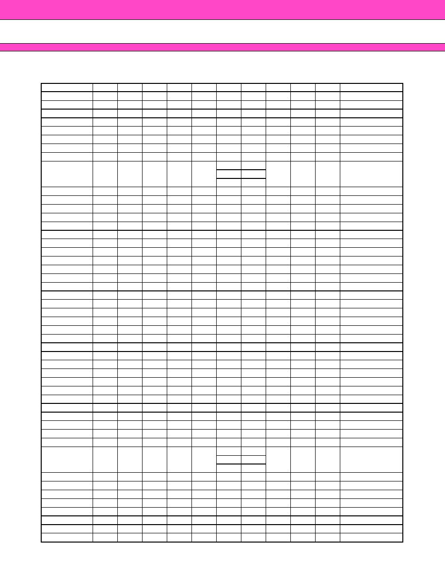
Sector Group Addresses
Sector Group
A
21
A
20
A
19
A
18
A
17
A
16
A
15
A
14
A
13
A
12
Sectors
SGA0
0
0
0
0
0
0
0
0
0
0
SA0
SGA1
0
0
0
0
0
0
0
0
0
1
SA1
SGA2
0
0
0
0
0
0
0
0
1
0
SA2
SGA3
0
0
0
0
0
0
0
0
1
1
SA3
SGA4
0
0
0
0
0
0
0
1
0
0
SA4
SGA5
0
0
0
0
0
0
0
1
0
1
SA5
SGA6
0
0
0
0
0
0
0
1
1
0
SA6
SGA7
0
0
0
0
0
0
0
1
1
1
SA7
SGA8
0
0
0
0
0
0
1
X
X
X
SA8 to SA10
1
0
1
1
SGA9
0
0
0
0
1
X
X
X
X
X
SA11 to SA14
SGA10
0
0
0
1
0
X
X
X
X
X
SA15 to SA18
SGA11
0
0
0
1
1
X
X
X
X
X
SA19 to SA22
SGA12
0
0
1
0
0
X
X
X
X
X
SA23 to SA26
SGA13
0
0
1
0
1
X
X
X
X
X
SA27 to SA30
SGA14
0
0
1
1
0
X
X
X
X
X
SA31 to SA34
SGA15
0
0
1
1
1
X
X
X
X
X
SA35 to SA38
SGA16
0
1
0
0
0
X
X
X
X
X
SA39 to SA42
SGA17
0
1
0
0
1
X
X
X
X
X
SA43 to SA46
SGA18
0
1
0
1
0
X
X
X
X
X
SA47 to SA50
SGA19
0
1
0
1
1
X
X
X
X
X
SA51 to SA54
SGA20
0
1
1
0
0
X
X
X
X
X
SA55 to SA58
SGA21
0
1
1
0
1
X
X
X
X
X
SA59 to SA62
SGA22
0
1
1
1
0
X
X
X
X
X
SA63 to SA66
SGA23
0
1
1
1
1
X
X
X
X
X
SA67 to SA70
SGA24
1
0
0
0
0
X
X
X
X
X
SA71 to SA74
SGA25
1
0
0
0
1
X
X
X
X
X
SA75 to SA78
SGA26
1
0
0
1
0
X
X
X
X
X
SA79 to SA82
SGA27
1
0
0
1
1
X
X
X
X
X
SA83 to SA86
SGA28
1
0
1
0
0
X
X
X
X
X
SA87 to SA90
SGA29
1
0
1
0
1
X
X
X
X
X
SA91 to SA94
SGA30
1
0
1
1
0
X
X
X
X
X
SA95 to SA98
SGA31
1
0
1
1
1
X
X
X
X
X
SA99 to SA102
SGA32
1
1
0
0
0
X
X
X
X
X
SA103 to SA106
SGA33
1
1
0
0
1
X
X
X
X
X
SA107 to SA110
SGA34
1
1
0
1
0
X
X
X
X
X
SA111 to SA114
SGA35
1
1
0
1
1
X
X
X
X
X
SA115 to SA118
SGA36
1
1
1
0
0
X
X
X
X
X
SA119 to SA122
SGA37
1
1
1
0
1
X
X
X
X
X
SA123 to SA126
SGA38
1
1
1
1
0
X
X
X
X
X
SA127 to SA130
SGA39
1
1
1
1
1
0
0
X
X
X
SA131 to SA133
0
1
1
0
SGA40
1
1
1
1
1
1
1
0
0
0
SA134
SGA41
1
1
1
1
1
1
1
0
0
1
SA135
SGA42
1
1
1
1
1
1
1
0
1
0
SA136
SGA43
1
1
1
1
1
1
1
0
1
1
SA137
SGA44
1
1
1
1
1
1
1
1
0
0
SA138
SGA45
1
1
1
1
1
1
1
1
0
1
SA139
SGA46
1
1
1
1
1
1
1
1
1
0
SA140
SGA47
1
1
1
1
1
1
1
1
1
1
SA141
MB84VD23581FJ
-70
18
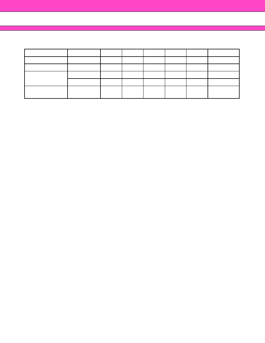
Flash Memory Autoselect Codes
Legend: L = V
IL
, H = V
IH
. See DC Characteristics for voltage levels.
*1 : Outputs 01h at protected sector group addresses and outputs 00h at unprotected sector group addresses.
*2 : A read cycle at address (BA) 01h outputs device code. When 227Eh was output, this indicates that there will
require two additional codes, called Extended Device Codes. Therefore the system may continue reading out
these Extended Device Codes at the address of (BA) 0Eh, as well as at (BA) 0Fh.
Type
A
21
to A
12
A
6
A
3
A
2
A
1
A
0
Code (HEX)
Manufacture's Code
BA
L
L
L
L
L
04h
Device Code
BA
L
L
L
L
H
227Eh
Extended Device
Code *
2
BA
L
H
H
H
L
2202h
BA
L
H
H
H
H
2201h
Sector Group
Protection
Sector Group
Addresses
L
L
L
H
L
01h*
1

MB84VD23581FJ
-70
19
Flash Memory Command Definitions
(Continued)
Command
Sequence
Bus
Write
Cycles
Req'd
First Bus
Write Cycle
Second Bus
Write Cycle
Third Bus
Write Cycle
Fourth Bus
Read/Write
Cycle
Fifth Bus
Write Cycle
Sixth Bus
Write Cycle
Addr.
Data
Addr.
Data
Addr.
Data
Addr.
Data
Addr.
Data
Addr.
Data
Read/Reset
1
XXXh
F0h
--
--
--
--
--
--
--
--
--
--
Read/Reset
3
555h
AAh
2AAh
55h
555h
F0h
RA
RD
--
--
--
--
Autoselect
3
555h
AAh
2AAh
55h
(BA)
555h
90h
--
--
--
--
--
--
Program
4
555h
AAh
2AAh
55h
555h
A0h
PA
PD
--
--
--
--
Program
Suspend
1
BA
B0h
--
--
--
--
--
--
--
--
--
--
Program
Resume
1
BA
30h
--
--
--
--
--
--
--
--
--
--
Chip Erase
6
555h
AAh
2AAh
55h
555h
80h
555h
AAh
2AAh
55h
555h
10h
Sector
Erase
6
555h
AAh
2AAh
55h
555h
80h
555h
AAh
2AAh
55h
SA
30h
Erase
Suspend
1
BA
B0h
--
--
--
--
--
--
--
--
--
--
Erase
Resume
1
BA
30h
--
--
--
--
--
--
--
--
--
--
Extended
Sector
Group
Protection *
2
4
XXXh
60h
SPA
60h
SPA
40h
SPA
SD
--
--
--
--
Set to
Fast Mode
3
555h
AAh
2AAh
55h
555h
20h
--
--
--
--
--
--
Fast
Program *
1
2
XXXh
A0h
PA
PD
--
--
--
--
--
--
--
--
Reset from
Fast
Mode *
1
2
BA
90h
XXXh
*
4
F0h
--
--
--
--
--
--
--
--
Query 1
(BA)
55h
98h
--
--
--
--
--
--
--
--
--
--
HiddenROM
Entry
3
555h
AAh
2AAh
55h
555h
88h
--
--
--
--
--
--
HiddenROM
Program *
3
4
555h
AAh
2AAh
55h
555h
A0h
(HRA)
PA
PD
--
--
--
--
HiddenROM
Exit *
3
4
555h
AAh
2AAh
55h
(HRBA)
555h
90h
XXXh
00h
--
--
--
--

MB84VD23581FJ
-70
20
(Continued)
*1: This command is valid during Fast Mode.
*2: This command is valid while RESET = V
ID
.
*3: This command is valid during HiddenROM mode.
*4: The data "00h" is also acceptable.
Notes :
∑
Address bits A
21
to A
11
= X = "H" or "L" for all address commands except or Program Address (PA),
Sector Address (SA), and Bank Address (BA), and Sector Group Address (SPA).
∑
Bus operations are defined in
s
DEVICE BUS OPERATION.
∑
RA
=
Address of the memory location to be read
PA
=
Address of the memory location to be programmed
Addresses are latched on the falling edge of the write pulse.
SA
=
Address of the sector to be erased. The combination of A
21
, A
20
, A
19
, A
18
, A
17
, A
16
, A
15
, A
14
, A
13
, and
A
12
will uniquely select any sector.
BA
=
Bank Address (A
21
, A
20
, A
19
)
∑
RD
=
Data read from location RA during read operation.
PD
=
Data to be programmed at location PA. Data is latched on the falling edge of write pulse.
∑
SPA
=
Sector group address to be protected. Set sector group address and (A
6
, A
3
, A
2
, A
1
, A
0
) =
(0, 0, 0, 1, 0).
SD
=
Sector group protection verify data. Output 01h at protected sector group addresses and output
00h at unprotected sector group addresses.
∑
HRA
=
Address of the HiddenROM area: 000000h to 00007Fh
∑
HRBA
=
Bank Address of the HiddenROM area (A
21
= A
20
= A
19
= V
IL
)
∑
The system should generate the following address patterns: 555h or 2AAh to addresses A
10
to A
0
∑
Both Read/Reset commands are functionally equivalent, resetting the device to the read mode.
∑
The command combinations not described in this table are illegal.

MB84VD23581FJ
-70
21
2.
AC Characteristics
∑ Read Only Operations Characteristics (Flash)
* : Test Conditions≠ Output Load : 1 TTL gate and 30 pF
Input rise and fall times: 5 ns
Input pulse levels: 0.0 V to V
CC
f
Timing measurement reference level
Input: 0.5◊V
CC
f
Output: 0.5◊V
CC
f
Parameter
Symbol
Condition
Value*
Unit
JEDEC
Standard
Min
Max
Read Cycle Time
t
AVAV
t
RC
--
70
--
ns
Address to Output Delay
t
AVQV
t
ACC
CEf = V
IL
OE = V
IL
--
70
ns
Chip Enable to Output Delay
t
ELQV
t
CE
f
OE = V
IL
--
70
ns
Output Enable to Output Delay
t
GLQV
t
OE
--
--
30
ns
Chip Enable to Output High-Z
t
EHQZ
t
DF
--
--
25
ns
Output Enable to Output High-Z
t
GHQZ
t
DF
--
--
25
ns
Output Hold Time From Addresses,
CEf or OE, Whichever Occurs First
t
AXQX
t
OH
--
0
--
ns
RESET Pin Low to Read Mode
--
t
READY
--
--
20
µs
MB84VD23581FJ
-70
22
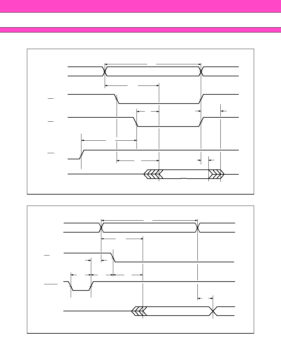
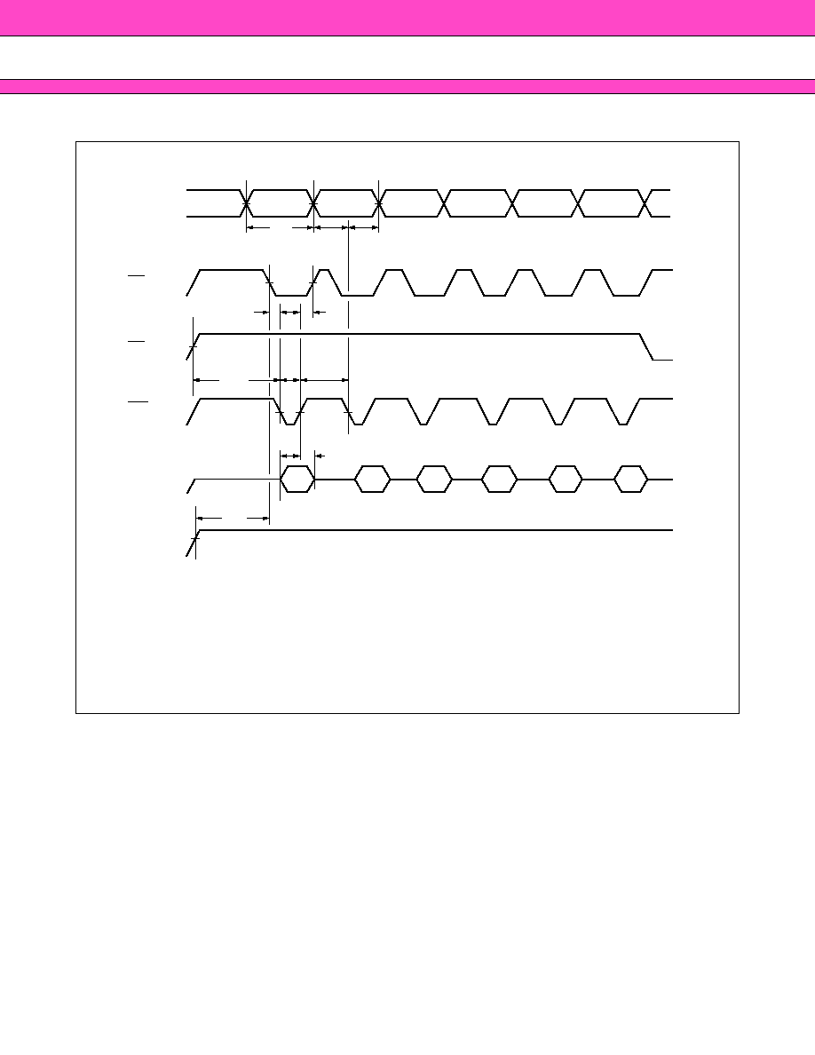
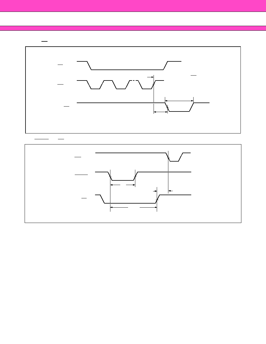
∑ Read Operation Timing Diagram (Flash)
∑ Hardware Reset/Read Operation Timing Diagram (Flash)
Address
Address Stable
High-Z
High-Z
CEf
OE
WE
Outputs
Outputs Valid
t
RC
t
ACC
t
OE
t
DF
t
CE
t
OH
t
OEH
Address
CEf
RESET
Outputs
High-Z
Outputs Valid
Address Stable
t
RC
t
ACC
t
RH
t
RP
t
RH
t
CE
t
OH

MB84VD23581FJ
-70
23
∑ Write/Erase/Program Operations (Flash)
(Continued)
Parameter
Symbol
Value
Unit
JEDEC
Standard
Min
Typ
Max
Write Cycle Time
t
AVAV
t
WC
70
ns
Address Setup Time
t
AVWL
t
AS
0
ns
Address Setup Time to OE Low During Toggle Bit
Polling
t
ASO
12
ns
Address Hold Time
t
WLAX
t
AH
45
ns
Address Hold Time from CEf or OE High During
Toggle Bit Polling
t
AHT
0
ns
Data Setup Time
t
DVWH
t
DS
30
ns
Data Hold Time
t
WHDX
t
DH
0
ns
Output
Enable Hold
Time
Read
t
OEH
0
ns
Toggle and Data Polling
10
ns
CEf High During Toggle Bit Polling
t
CEPH
20
ns
OE High During Toggle Bit Polling
t
OEPH
20
ns
Read Recover Time Before Write
t
GHWL
t
GHWL
0
ns
Read Recover Time Before Write
t
GHEL
t
GHEL
0
ns
CEf Setup Time
t
ELWL
t
CS
0
ns
WE Setup Time
t
WLEL
t
WS
0
ns
CEf Hold Time
t
WHEH
t
CH
0
ns
WE Hold Time
t
EHWH
t
WH
0
ns
Write Pulse Width
t
WLWH
t
WP
35
ns
CEf Pulse Width
t
ELEH
t
CP
35
ns
Write Pulse Width High
t
WHWL
t
WPH
25
ns
CEf Pulse Width High
t
EHEL
t
CPH
25
ns
Programming Operation
t
WHWH1
t
WHWH1
6
µ
s
Sector Erase Operation *
1
t
WHWH2
t
WHWH2
0.5
s
V
CC
f Setup Time
t
VCS
50
µ
s
Rise Time to V
ID
*
2
t
VIDR
500
ns
Rise Time to V
ACC
*
3
t
VACCR
500
ns
Voltage Transition Time *
2
t
VLHT
4
µ
s
Write Pulse Width *
2
t
WPP
100
µ
s
MB84VD23581FJ
-70
24
(Continued)
*1: This does not include preprogramming time.
*2: This timing is for Sector Group Protection operation.
*3: This timing is for Accelerated Program operation.
Parameter
Symbol
Value
Unit
JEDEC
Standard
Min
Typ
Max
OE Setup Time to WE Active *
2
t
OESP
4
µ
s
CEf Setup Time to WE Active *
2
t
CSP
4
µ
s
Recover Time from RY/BY
t
RB
0
ns
RESET Pulse Width
t
RP
500
ns
RESET High Level Period Before Read
t
RH
200
ns
Program/Erase Valid to RY/BY Delay
t
BUSY
90
ns
Delay Time from Embedded Output Enable
t
EOE
70
ns
Erase Time-out Time
t
TOW
50
µ
s
Erase Suspend Transition Time
t
SPD
20
µ
s
MB84VD23581FJ
-70
25
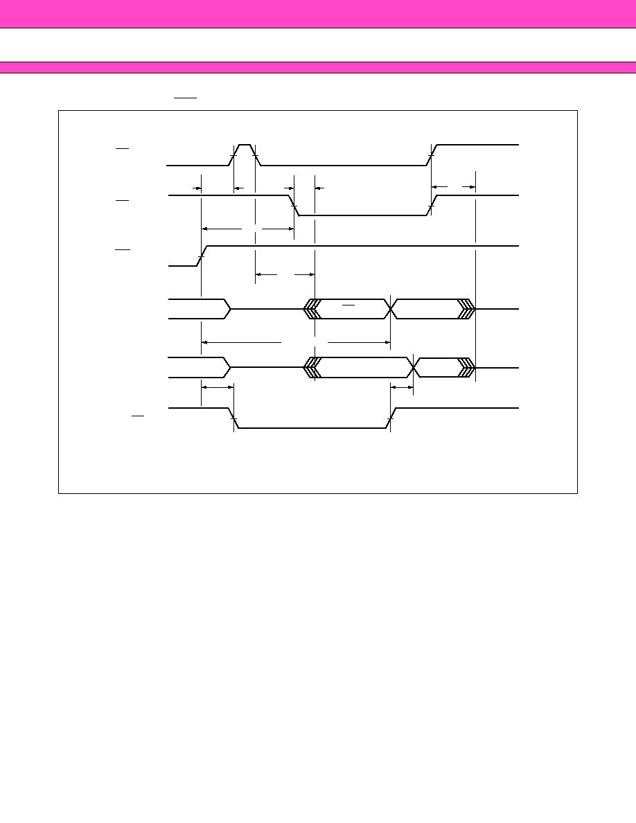
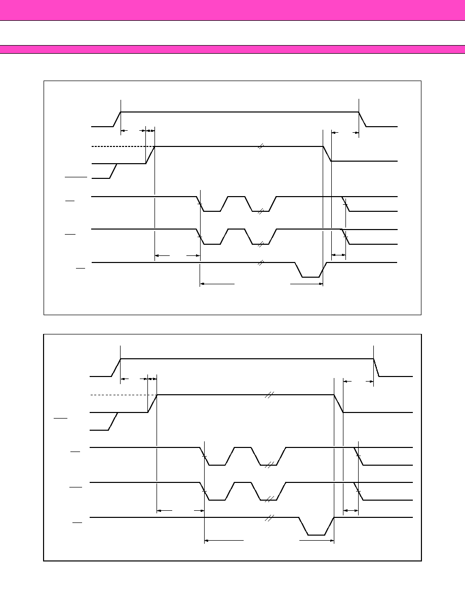
∑ Write Cycle (WE control) (Flash)
Notes :
∑
PA is address of the memory location to be programmed.
∑
PD is data to be programmed at word address.
∑
DQ
7
is the output of the complement of the data written to the device.
∑
D
OUT
is the output of the data written to the device.
∑
Figure indicates last two bus cycles out of four bus cycle sequence.
Address
Data
CEf
OE
WE
3rd Bus Cycle
Data Polling
555h
PA
A0h
PD
DQ
7
D
OUT
D
OUT
PA
t
WC
t
AS
t
AH
t
RC
t
CE
t
WHWH1
t
WPH
t
WP
t
GHWL
t
DS
t
DH
t
DF
t
OH
t
OE
t
CS
t
CH
MB84VD23581FJ
-70
26
∑ Write Cycle (CEf control) (Flash)
Notes :
∑
PA is address of the memory location to be programmed.
∑
PD is data to be programmed at word address.
∑
DQ
7
is the output of the complement of the data written to the device.
∑
D
OUT
is the output of the data written to the device.
∑
Figure indicates last two bus cycles out of four bus cycle sequence.
Address
Data
WE
OE
CEf
3rd Bus Cycle
Data Polling
555h
PA
A0h
PD
DQ
7
D
OUT
PA
t
WC
t
AS
t
AH
t
WHWH1
t
CPH
t
CP
t
GHEL
t
DS
t
DH
t
WS
t
WH
MB84VD23581FJ
-70
27
∑ AC Waveforms Chip/Sector Erase Operations (Flash)
Address
Data
V
CC
f
CEf
OE
WE
555h
2AAh
555h
555h
2AAh
SA*
t
WC
t
AS
t
AH
t
CS
t
GHWL
t
CH
t
WP
t
DS
t
VCS
t
DH
t
WPH
AAh
55h
80h
AAh
55h
10h/
30h
30h for Sector Erase
* : SA is the sector address for Sector Erase. Addresses
=
555h (Word) for Chip Erase.
MB84VD23581FJ
-70
28
∑ AC Waveforms for Data Polling during Embedded Algorithm Operations (Flash)
* : DQ
7
=
Valid Data (the device has completed the Embedded operation) .
t
OEH
t
CH
t
OE
t
CE
t
DF
t
BUSY
t
EOE
t
WHWH1 or 2
CEf
DQ
7
DQ
6
to DQ
0
RY/BY
DQ
7
DQ
7
=
Valid Data
DQ
6
to DQ
0
=
Output Flag
DQ
6
to DQ
0
Valid Data
OE
WE
High-Z
High-Z
Data
Data
*
MB84VD23581FJ
-70
29
∑ AC Waveforms for Toggle Bit during Embedded Algorithm Operations (Flash)
t
DH
t
OE
t
CE
CEf
WE
OE
DQ
6
/DQ
2
Address
RY/BY
Data
Toggle
Data
Toggle
Data
Toggle
Data
Stop
Toggling
Output
Valid
*
t
BUSY
t
OEH
t
OEH
t
OEPH
t
AHT
t
AHT
t
ASO
t
AS
t
CEPH
* : DQ
6
stops toggling (the device has completed the Embedded operation).
MB84VD23581FJ
-70
30
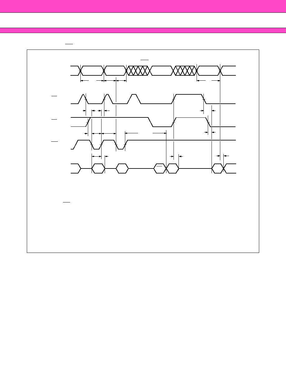
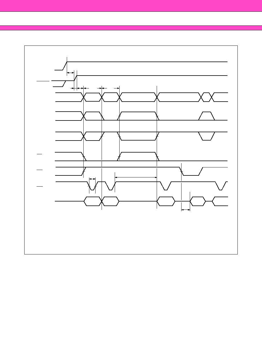
∑ Bank-to-bank Read/Write Timing Diagram (Flash)
CEf
DQ
WE
Address
BA1
BA1
BA1
BA2
(555h)
BA2
(PA)
BA2
(PA)
OE
Valid
Output
Valid
Output
Valid
Output
Status
Valid
Intput
Valid
Intput
t
RC
t
RC
t
RC
t
RC
t
WC
t
WC
t
AHT
t
AS
t
AS
t
AH
t
ACC
t
CE
t
OE
t
OEH
t
WP
t
GHWL
t
DS
t
DF
t
DH
t
DF
t
CEPH
Read
Command
Command
Read
Read
Read
(A0h)
(PD)
Note : This is example of Read for Bank 1 and Embedded Algorithm (program) for Bank 2.
BA1 : Address corresponding to Bank 1
BA2 : Address corresponding to Bank 2
MB84VD23581FJ
-70
31
∑ RY/BY Timing Diagram during Write/Erase Operations (Flash)
∑ RESET, RY/BY Timing Diagram (Flash)
CEf
RY/BY
WE
Rising edge of the last WE signal
t
BUSY
Entire programming
or erase operations
t
RP
t
RB
t
READY
RY/BY
WE
RESET
MB84VD23581FJ
-70
32
∑ Temporary Sector Unprotection (Flash)
∑ Acceleration Mode Timing Diagram (Flash)
Unprotection period
t
VLHT
t
VLHT
t
VCS
t
VLHT
t
VIDR
Program or Erase Command Sequence
V
CC
f
V
ID
V
IH
WE
RY/BY
CEf
RESET
V
IH
WP/ACC
V
CC
f
CEf
WE
RY/BY
t
VLHT
Program Command Sequence
t
VLHT
t
VCS
t
VACCR
VACC
t
VLHT
Acceleration period
MB84VD23581FJ
-70
33
∑ Extended Sector Group Protection (Flash)
SPAX : Sector Group Address to be protected
SPAY : Next Sector Group Address to be protected
TIME-OUT : Time-Out window
=
250
µ
s (Min)
V
CC
f
WE
OE
CEf
RESET
t
WC
t
WC
t
VLHT
t
VIDR
t
VCS
TIME-OUT
SPAX
SPAX
SPAY
t
WP
t
OE
60h
01h
40h
60h
60h
Data
Address
A
6
, A
3
,
A
2
, A
0
A
1

MB84VD23581FJ
-70
34
s
s
s
s
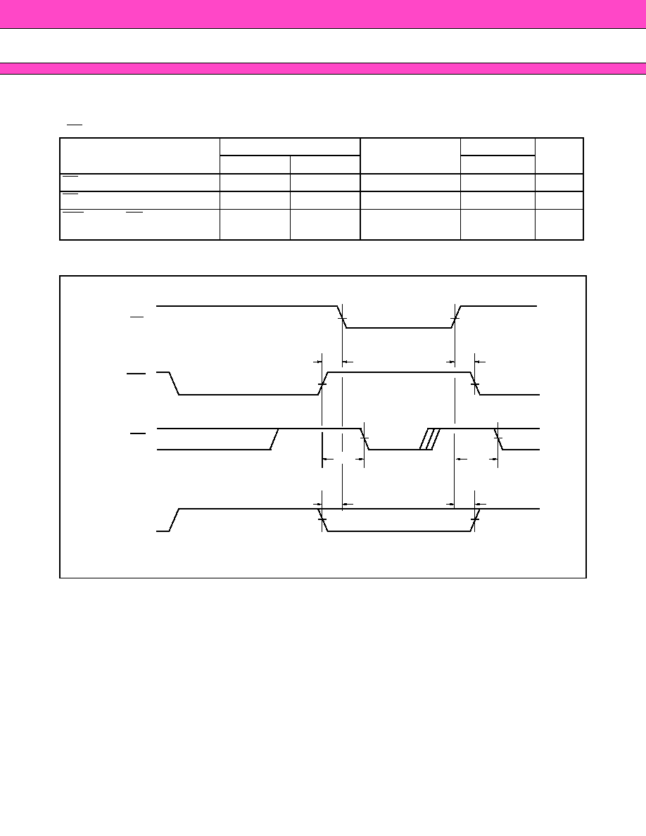
64 M FCRAM CHARACTERISTICS for MCP
1.
FCRAM Power Down Program Key Table
Basic Key Table
Available Key Table
Definition
A
16
A
17
A
19
A
20
A
21
KEY
Mode Select
Area Select
A
19
A
20
A
21
AREA
L
L
L
BOTTOM *
2
L
H
X
RESERVED
H
L
X
RESERVED
H
H
H
TOP *
3
A
16
A
17
MODE
L
L
NAP *
4
L
H
RESERVED
H
L
16M Partial
H
H
SLEEP *
4,
*
5
MODE
A
16
A
17
A
19
A
20
A
21
Data Retention
Area
Mode Select
Area Select
NAP
L
L
X
X
X
None
16M Partial
H
L
L
L
L
Bottom 16M only
H
L
H
H
H
Top 16M only
SLEEP
H
H
X
X
X
None
*1 : The Power Down Program can be performed one time after compliance of Power-up timings and it
should not be re-programmed after regular Read or Write.
Unspecified addresses, A
18
and A
15
to A
0
, can be either High or Low during the programming.
The RESERVED key should not be used.
*2 : BOTTOM area is from the lowest address location. (i.e., A
21
to A
0
= L)
*3 : TOP area is from the highest address location. (i.e., A
21
to A
0
= H)
*4 : NAP and SLEEP do not retain the data and Area Select is ignored.
*5 : Default state. Power Down Program to this SLEEP mode can be omitted.
MB84VD23581FJ
-70
35
2.
AC Charactaristics
∑ READ OPERATION (FCRAM)
*1 : The output load is 30 pF.
*2 : The output load is 5 pF.
*3 : The t
CE
is applicable if OE is brought to Low before CE1r goes Low and is also applicable if actual value of both
or either t
ASO
or t
CLOL
is shorter than specified value.
*4 : Applicable only to A
0
and A
1
when both CE1r and OE are kept at Low for the address access.
*5 : Applicable if OE is brought to Low before CE1r goes Low.
*6 : The t
ASO
, t
CLOL(Min)
and t
OP(Min)
are reference values when the access time is determined by t
OE
.
If actual value of each parameter is shorter than specified minimum value, t
OE
become longer by the amount
of subtracting actual value from specified minimum value.
For example, if actual t
ASO
, t
ASO(actual)
, is shorter than specified minimum value, t
ASO(Min)
, during OE control access
(i.e., CE1r stays Low), the t
OE
become t
OE(Max)
+ t
ASO(Min)
≠ t
ASO(actual)
.
*7 : The t
ASO(ABS)
and t
OP(ABS)
is the absolute minimum value during OE control access.
*8 : The t
AX
is applicable when both A
0
and A
1
are switched from previous state.
*9 : If actual value of either t
CLOL
or t
OP
is shorter than specified minimum value, both t
OLAH
and t
OLCH
become t
RC(Min)
≠
t
CLOL(actual)
or t
RC(Min)
≠ t
OP(actual)
.
*10 : Maximum value is applicable if CE1r is kept at Low.
Parameter Symbol
Value
Unit
Notes
Min
Max
Read Cycle Time
t
RC
70
--
ns
Chip Enable Access Time
t
CE
--
65
ns
*1,*3
Output Enable Access Time
t
OE
--
40
ns
*1
Address Access Time
t
AA
--
65
ns
*1,*4
Output Data Hold Time
t
OH
5
--
ns
*1
CE1r Low to Output Low-Z
t
CLZ
5
--
ns
*2
OE Low to Output Low-Z
t
OLZ
0
--
ns
*2
CE1r High to Output High-Z
t
CHZ
--
20
ns
*2
OE High to Output High-Z
t
OHZ
--
20
ns
*2
Address Setup Time to CE1r Low
t
ASC
≠5
--
ns
*5
Address Setup Time to OE
t
ASO
25
--
ns
*3,*6
t
ASO[ABS]
10
--
ns
*7
LB / UB Setup Time to CE1r Low
t
BSC
≠5
--
ns
*5
LB / UB Setup Time to OE Low
t
BSO
10
--
ns
Address Invalid Time
t
AX
--
5
ns
*4,*8
Address Hold Time from CE1r Low
t
CLAH
70
--
ns
*4
Address Hold Time from OE Low
t
OLAH
45
--
ns
*4,*9
Address Hold Time from CE1r High
t
CHAH
≠5
--
ns
Address Hold Time from OE High
t
OHAH
≠5
--
ns
LB / UB Hold Time from CE1r High
t
CHBH
≠5
--
ns
LB / UB Hold Time from OE High
t
OHBH
≠5
--
ns
CE1r Low to OE Low Delay Time
t
CLOL
25
1000
ns
*3,*6,*9,*10
OE Low to CE1r High Delay Time
t
OLCH
45
--
ns
*9
CE1r High Pulse Width
t
CP
12
--
ns
OE High Pulse Width
t
OP
25
1000
ns
*6,*9,*10
t
OP[ABS]
12
--
ns
*7
MB84VD23581FJ
-70
36
∑ WRITE OPERATION (FCRAM)
*1 : Minimum value must be equal or greater then the sum of actual t
CW
(or t
WP
) and t
WRC
(or t
WR
).
*2 : New write address is valid from either CE1r or WE is bought to High.
*3 : The t
OEH
is specified from end of t
WC(Min)
. The t
OEH(Min)
is a reference value when the access time is determined
by t
OE
.
If actual value, t
OEH(actual)
is shorter than specified minimum value, t
OE
become longer by the amount of
subtracting actual value from specified minimum value.
*4 : The t
OEH(Max)
is applicable if CE1r is kept at Low and both WE and OE are kept at High.
*5 : The t
OEH(ABS
)
is the absolute minimum value if write cycle is termnated by WE and CE1r stays Low.
*6 : t
OHCL(Min)
must be satisfied if read operation is not performed prior to write operation.
In case OE is disabled after t
OHCL(Min)
, WE Low must be asserted after t
RC(Min)
from CE1r Low.
In other words, read operation is initiated if t
OHCL (Min)
is not satisfied.
*7 : Applicable if CE1r stays Low after read operation.
*8 : t
CW
and t
WP
is applicable if write operation is initiated by CE1r and WE, respectively.
*9 : t
WRC
and t
WR
is applicable if write operation is terminated by CE1r and WE, respectively.
The t
WR(Min)
can be ignored if CE1r is brought to High together or after WE is brought to High.
In such case, the t
CP(Min)
must be satisfied.
Parameter Symbol
Value
Unit
Notes
Min
Max
Write Cycle Time
t
WC
70
--
ns
*1
Address Setup Time
t
AS
0
--
ns
*2
Address Hold Time
t
AH
35
--
ns
*2
CE1r Write Setup Time
t
CS
0
1000
ns
CE1r Write Hold Time
t
CH
0
1000
ns
WE Setup Time
t
WS
0
--
ns
WE Hold Time
t
WH
0
--
ns
LB and UB Setup Time
t
BS
≠5
--
ns
LB and UB Hold Time
t
BH
≠5
--
ns
OE Setup Time
t
OES
0
1000
ns
*3
OE Hold Time
t
OEH
25
1000
ns
*3, *4
t
OEH[ABS]
12
--
ns
*5
OE High to CE1r Low Setup Time
t
OHCL
≠5
--
ns
*6
OE High to Address Hold Time
t
OHAH
≠5
--
ns
*7
CE1r Write Pulse Width
t
CW
45
--
ns
*1, *8
WE Write Pulse Width
t
WP
45
--
ns
*1, *8
CE1r Write Recovery Time
t
WRC
10
--
ns
*1, *9
WE Write Recovery Time
t
WR
10
1000
ns
*1, *3, *9
Data Setup Time
t
DS
15
--
ns
Data Hold Time
t
DH
0
--
ns
CE1r High Pulse Width
t
CP
12
--
ns
*9
MB84VD23581FJ
-70
37
∑ POWER DOWN and POWER DOWN PROGRAM PARAMETERS (FCRAM)
* : Applicable to Power Down Program.
∑ OTHER TIMING PARAMETERS (FCRAM)
*1 : It may write some data into any address location if t
CHWX
is not satisfied.
*2 : Must satisfy t
CHH(Min)
after t
C2LH(Min)
.
*3 : Requires Power Down mode entry and exit after t
C2HL
.
*4 : The input Trasition Time(t
T
) at AC testing is 5 ns as shown in below. If actual t
T
is longer than 5 ns, it may violate
AC specification of some timing parameters.
∑ AC TEST CONDITIONS (FCRAM)
Parameter Symbol
Value
Unit
Note
Min
Max
CE2r Low Setup Time for Power Down Entry
t
CSP
10
--
ns
CE2r Low Hold Time after Power Down Entry
t
C2LP
70
--
ns
CE1r High Hold Time following CE2r High after
Power Down Exit (SLEEP mode only)
t
CHH
350
--
µ
s
CE1r High Setup Time following CE2r High after
Power Down Exit (Except for SLEEP mode)
t
CHHN
1
--
µ
s
CE1r High Setup Time following CE2r High after
Power Down Exit
t
CHS
10
--
ns
CE1r High to PE Low Setup Time
t
EPS
70
--
ns
*
PE Power Down Program Pulse Width
t
EP
70
--
ns
*
PE High to CE1r Low Hold Time
t
EPH
70
--
ns
*
Address Setup Time to PE High
t
EAS
15
--
ns
*
Address Setup Time from PE High
t
EAH
0
--
ns
*
Parameter Symbol
Value
Unit
Note
Min
Max
CE1r High to OE Invalid Time for Standby Entry
t
CHOX
10
--
ns
CE1r High to WE Invalid Time for Standby Entry
t
CHWX
10
--
ns
*1
CE2r Low Hold Time after Power-up
t
C2LH
50
--
µ
s
*2
CE2r High Hold Time after Power-up
t
C2HL
50
--
µ
s
*3
CE1r High Hold Time following CE2r High after
Power-up
t
CHH
350
--
µ
s
*2
Input Transition Time
t
T
1
25
ns
*4
Description
Symbol
Test Setup
Value
Unit
Note
Input High Level
V
IH
V
CC
r = 2.7 V to 3.1 V
2.3
V
Input Low Level
V
IL
V
CC
r = 2.7 V to 3.1 V
0.4
V
Input Timing Measurement Level
V
REF
V
CC
r = 2.7 V to 3.1 V
1.3
V
Input Transition Time
t
T
Between V
IL
and V
IH
5
ns
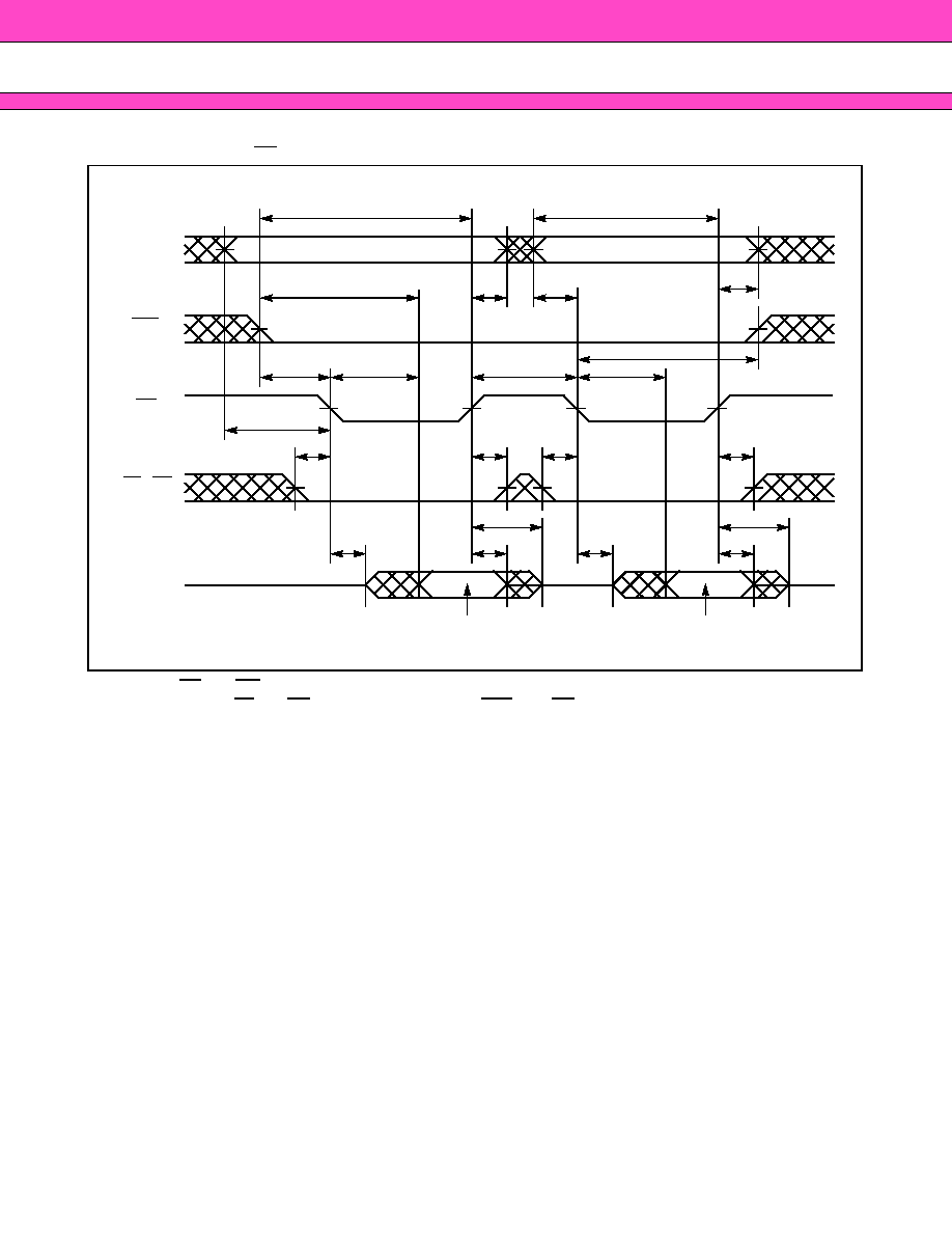
MB84VD23581FJ
-70
38
∑ READ Timing #1 (OE Control Access) (FCRAM)
Note : CE2r, PE and WE must be High for entire read cycle.
Either or both LB and UB must be Low when both CE1r and OE are Low.
t
CE
Valid Data Output
Address
CE1r
DQ
(Output)
LB / UB
t
OHZ
t
OHZ
t
OE
t
RC
t
OLZ
t
OLZ
t
OHAH
t
OP
Address Valid
t
ASO
t
OE
Valid Data Output
Address Valid
t
CLOL
t
RC
t
OH
t
OH
t
OHAH
t
ASO
t
OLCH
OE
t
BSO
t
BSO
t
OHBH
t
OHBH
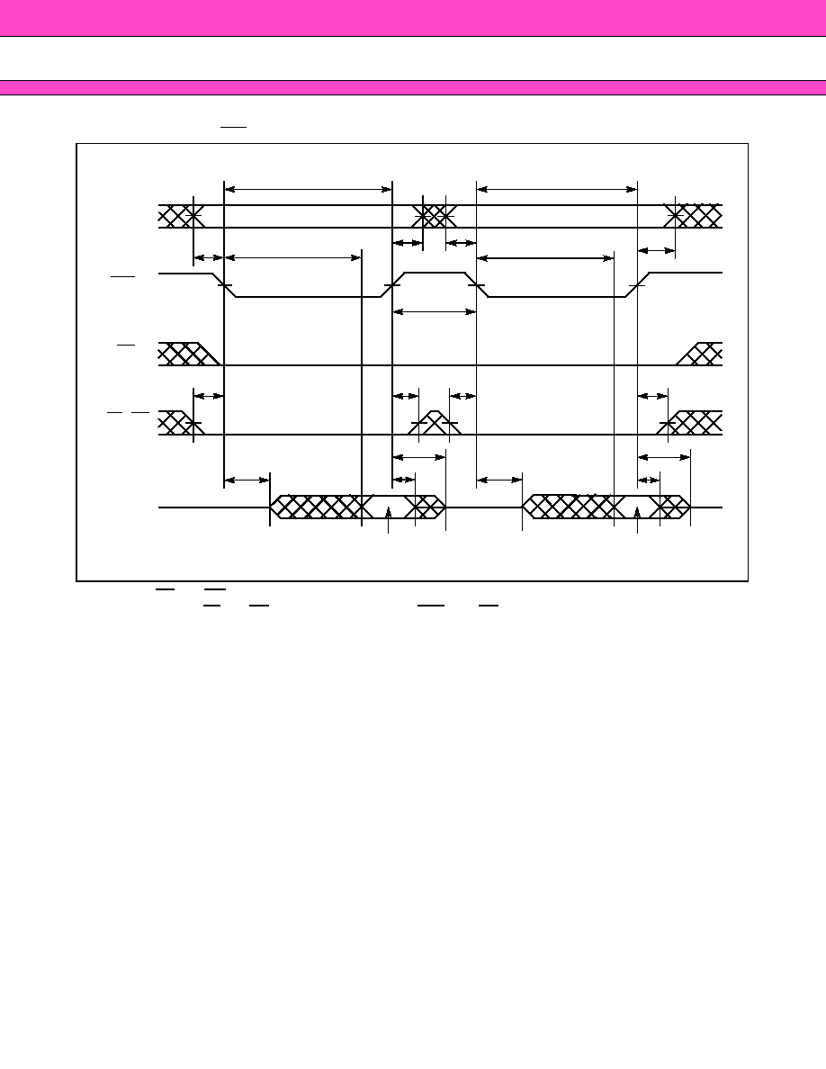
MB84VD23581FJ
-70
39
∑ READ Timing #2 (CE1r Control Access) (FCRAM)
Note : CE2r, PE and WE must be High for entire read cycle.
Either or both LB and UB must be Low when both CE1r and OE are Low.
t
CE
t
CE
Valid Data Output
Address
CE1r
DQ
(Output)
OE
t
CHZ
t
CHZ
t
RC
t
CLZ
t
CHAH
t
CP
Address Valid
t
ASC
Valid Data Output
Address Valid
t
ASC
t
CHAH
t
CLZ
t
OH
t
OH
t
RC
LB / UB
t
BSC
t
BSC
t
CHBH
t
CHBH
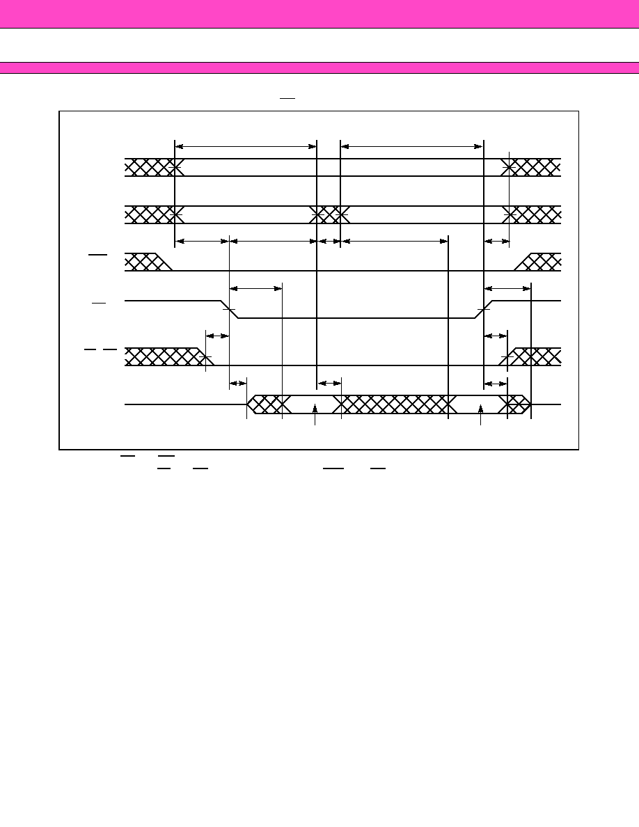
MB84VD23581FJ
-70
40
∑ READ Timing #3 (Address Access after OE Control Access) (FCRAM)
Note : CE2r, PE and WE must be High for entire read cycle.
Either or both LB and UB must be Low when both CE1r and OE are Low.
Valid Data Output
Address
(A
2
to A
0
)
CE1r
DQ
(Output)
OE
t
OHZ
t
OE
t
RC
t
OLZ
t
OLAH
Address Valid
t
AX
Valid Data Output
Address Valid
t
RC
t
OH
t
OH
t
OHAH
t
ASO
t
AA
Address
(A
21
to A
3
)
Address Valid
Address Valid (No change)
LB / UB
t
BSO
t
OHBH
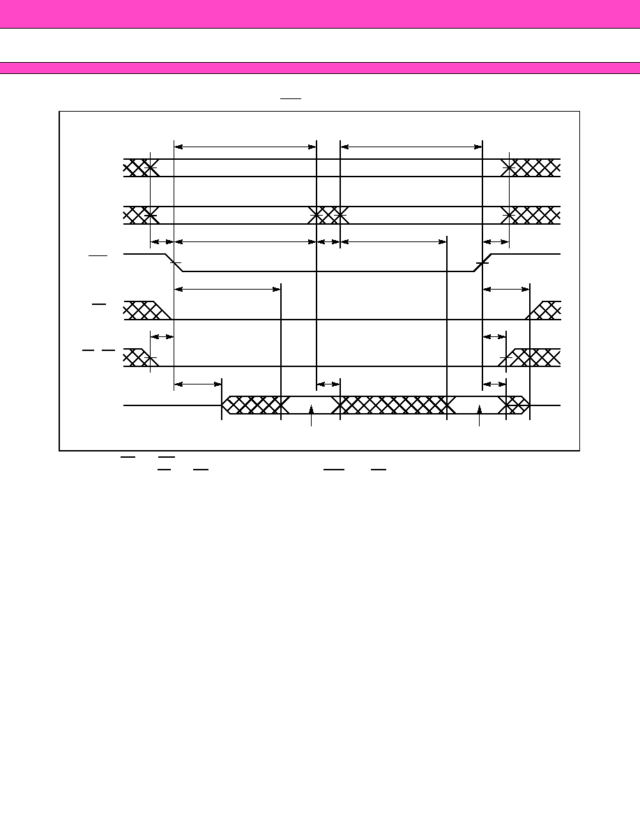
MB84VD23581FJ
-70
41
∑ READ Timing #4 (Address Access after CE1r Control Access) (FCRAM)
Note : CE2r, PE and WE must be High for entire read cycle.
Either or both LB and UB must be Low when both CE1r and OE are Low.
t
AA
t
CE
Valid Data Output
Address
(A
2
to A
0
)
CE1r
DQ
(Output)
OE
t
CHZ
t
RC
t
CLZ
t
AX
Address Valid
Valid Data Output
Address Valid
t
ASC
t
CHAH
t
OH
t
OH
t
RC
t
CLAH
Address
(A
21
to A
3
)
Address Valid
Address Valid (No change)
LB / UB
t
BSC
t
CHBH
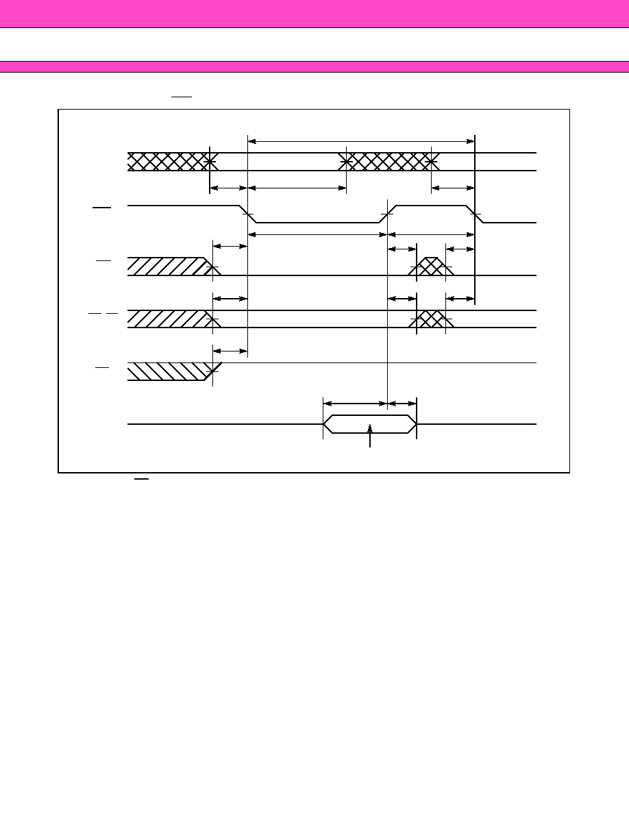
MB84VD23581FJ
-70
42
∑ WRITE Timing #1 (CE1r Control) (FCRAM)
Note : CE2r and PE must be High for write cycle.
t
AS
Valid Data Input
Address
CE1r
DQ
(Input)
WE
t
DH
t
DS
t
WC
t
WRC
t
WS
t
CW
t
WH
UB, LB
t
BH
t
BS
Address Valid
t
AS
t
AH
t
WS
t
BS
OE
t
OHCL
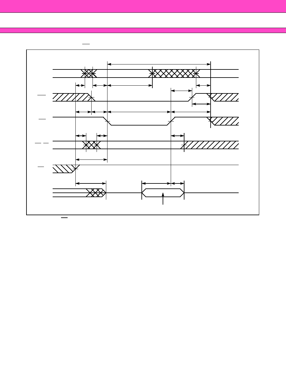
MB84VD23581FJ
-70
43
∑ WRITE Timing #2-1 (WE Control,Single Write Operetion) (FCRAM)
Note : CE2r and PE must be High for write cycle.
t
AS
Address
WE
CE1r
t
WC
t
CS
t
WP
UB, LB
t
BS
Address Valid
t
AS
t
AH
t
WR
t
BH
t
CP
Valid Data Input
DQ
(Input)
t
DH
t
DS
OE
t
OES
t
OHCL
t
OHAH
t
OHZ
t
CH
t
OHBH
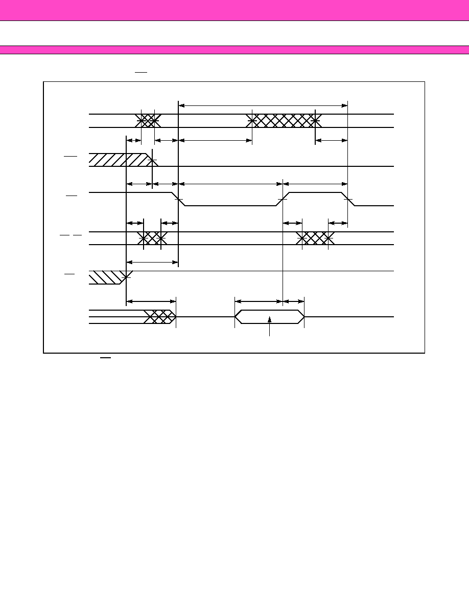
MB84VD23581FJ
-70
44
∑ WRITE Timing #2-2 (WE Control,Continuous Write Operetion) (FCRAM)
Note : CE2r and PE must be High for write cycle.
t
AS
Address
WE
CE1r
t
WC
t
CS
t
WP
UB, LB
Address Valid
t
AS
t
AH
t
WR
t
BH
t
BS
Valid Data Input
DQ
(Input)
t
DH
t
DS
OE
t
OES
t
OHCL
t
OHAH
t
OHZ
t
BS
t
BH
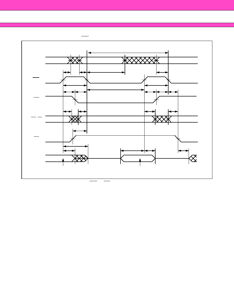
MB84VD23581FJ
-70
45
∑ READ / WRITE Timing #1-1 (CE1r Control) (FCRAM)
Note : Write address is valid from either CE1r or WE of last falling edge.
Read Data Output
Address
CE1r
DQ
WE
t
WC
t
CW
OE
t
OHCL
UB, LB
t
BS
t
CHAH
t
CP
Write Address
t
AS
t
AH
Write Data Input
t
DS
t
CHZ
t
OH
t
WRC
t
CLOL
t
BH
t
ASC
Read Address
t
WS
t
WH
t
WS
t
WH
t
DH
t
OLZ
t
CHBH
t
BSO
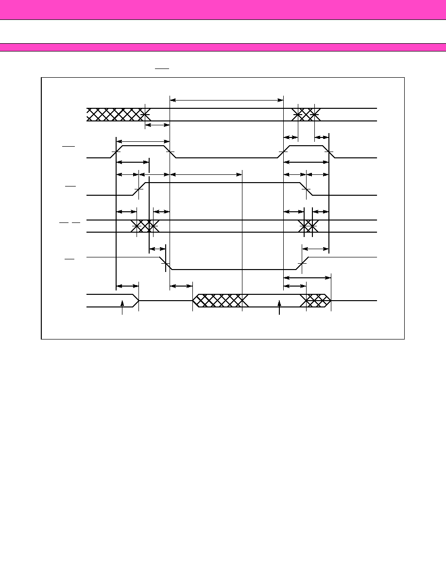
MB84VD23581FJ
-70
46
∑ READ / WRITE Timing #1-2 (CE1r Control) (FCRAM)
Note : The t
OEH
is specified from the time satisfied both t
WRC
and t
WR
(Min).
Read Data Output
Address
CE1r
DQ
WE
t
RC
t
CP
t
WS
OE
t
WH
t
OHCL
t
OEH
UB, LB
t
BH
t
BS
Write Address
t
CHAH
t
WRC
(Min)
Write Data Input
t
DH
t
OH
t
AS
t
WS
Read Address
t
CHZ
t
CLZ
t
CE
t
ASC
t
WH
t
WRC
t
BSC
t
CHBH
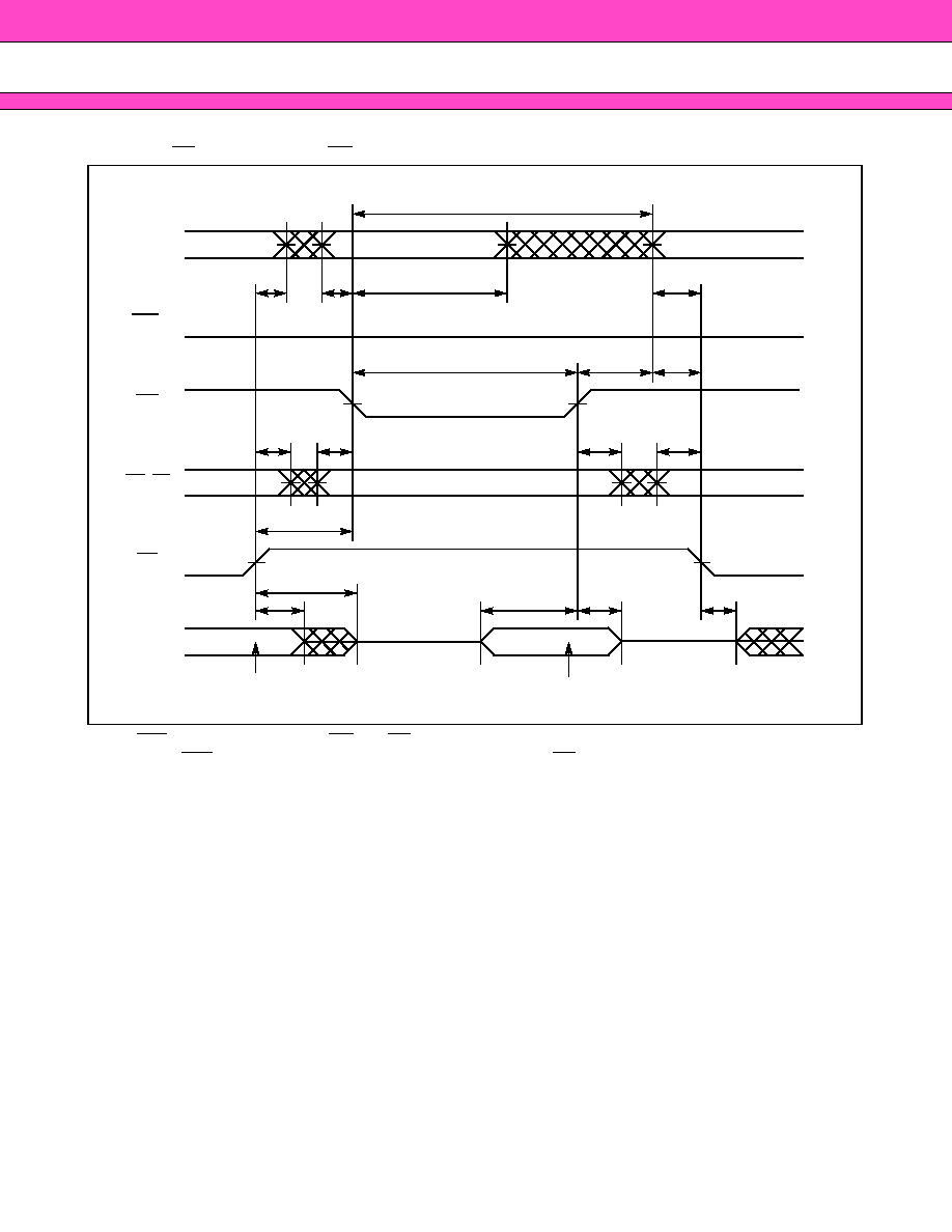
MB84VD23581FJ
-70
47
∑ READ(OE Control) / WRITE(WE Control) Timing #2-1 (FCRAM)
Note : CE1r can be tied to Low for WE and OE controlled operation.
When CE1r is tied to Low, output is exclusively controlled by OE.
t
WR
Read Data Output
Address
CE1r
DQ
WE
t
WC
t
WP
OE
t
OES
UB, LB
t
BS
Write Address
t
AS
t
AH
Write Data Input
t
DH
t
DS
t
OHZ
t
OH
Low
t
OEH
t
BH
t
ASO
t
OHAH
Read Address
t
OLZ
t
OHBH
t
BSO
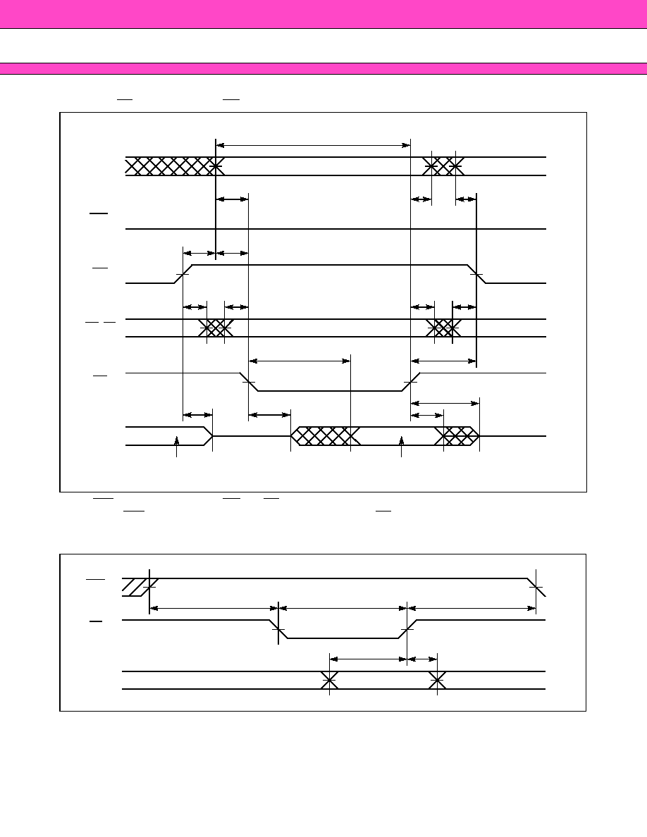
MB84VD23581FJ
-70
48
∑ READ(OE Control) / WRITE(WE Control) Timing #2-2
Note : CE1
r
can be tied to Low for WE and OE controlled operation.
When CE1
r
is tied to Low, output is exclusively controlled by OE.
∑ POWER DOWN PROGRAM Timing (FCRAM)
Note : CE2r must be High for Power Down Programming.
Any other inputs not specified above can be either High or Low.
Read Data Output
Address
CE1r
DQ
WE
Low
OE
t
OES
t
OEH
UB, LB
t
BH
Write Address
Write Data Input
t
DH
t
OH
t
AS
Read Address Valid
t
OHZ
t
OLZ
t
OE
t
OHAH
t
ASO
t
RC
t
WR
t
OHBH
t
BS
t
BSO
t
EPS
CE1r
PE
t
EP
t
EPH
t
EAS
Address
(A
20
to A
16
)
KEY
t
EAH
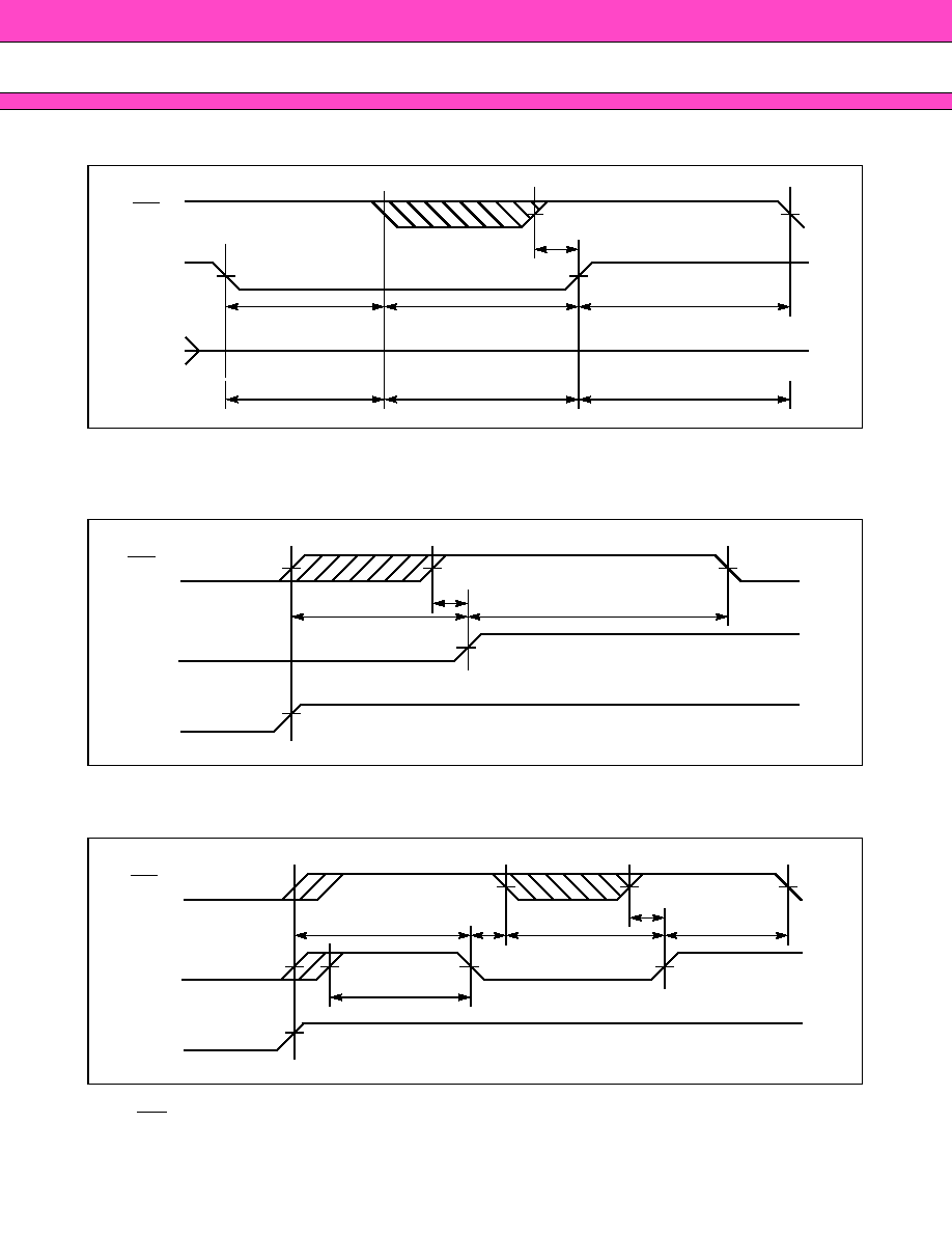
MB84VD23581FJ
-70
49
∑ POWER DOWN Entry and Exit Timing (FCRAM)
Note : This Power Down mode can be also used for Power-up #2 below except that t
CHHN
can not be used at Power-
up timing.
∑ POWER-UP Timing #1 (FCRAM)
Note : The t
C2LH
specifies after V
CC
r reaches specified minimum level.
∑ POWER-UP Timing #2 (FCRAM)
Note : The t
C2HL
specifies from CE2r Low to High transition after V
CC
r reaches specified minimum level.
CE1r must be brought to High prior to or together with CE2r Low to High transition.
t
CSP
CE1r
Power Down Entry
CE2r
t
C2LP
t
CHH
(t
CHHN
)
Power Down Mode
Power Down Exit
t
CHS
DQ
High-Z
t
C2LH
CE1r
V
CC
r
V
CC
r
Min
0 V
CE2r
t
CHH
t
CHS
t
C2HL
CE1r
V
CC
r
V
CC
r
Min
0 V
CE2r
t
CHH
t
CHS
t
CSP
t
C2LP
t
C2HL
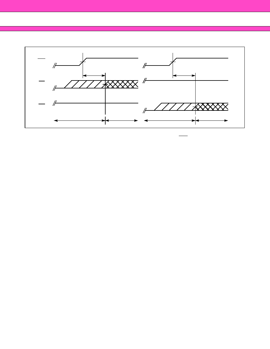
MB84VD23581FJ
-70
50
∑ Standby Entry Timing after Read or Write (FCRAM)
Note : Both t
CHOX
and t
CHWX
define the earliest entry timing for Standby mode. If either of timing is not satisfied, it
takes t
RC
(Min) period from either last address transition of A
0
and A
1
, or CE1r Low to High transition.
t
CHOX
CE1r
OE
WE
Active (Read)
Standby
Active (Write)
Standby
t
CHWX
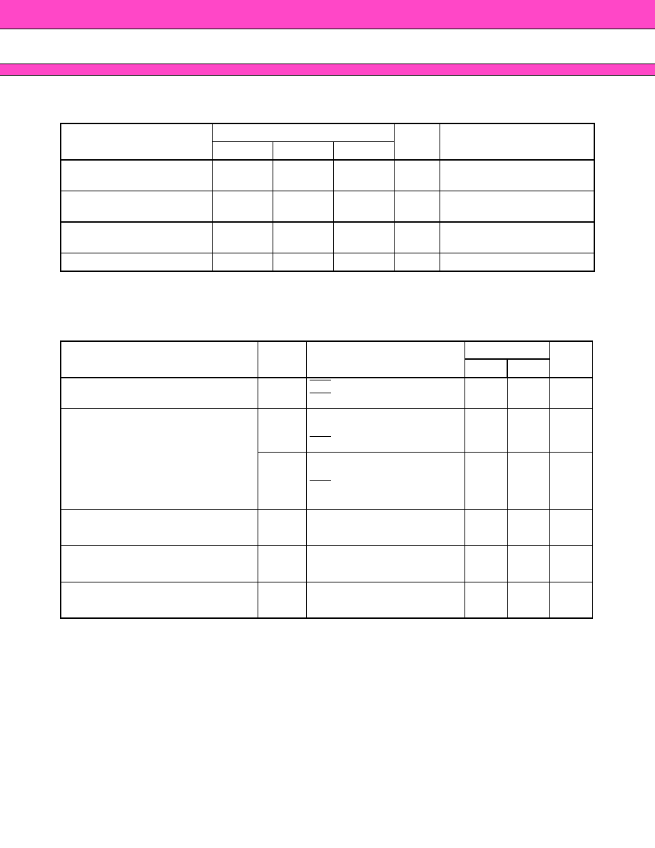
MB84VD23581FJ
-70
51
s
s
s
s
ERASE AND PROGRAMMING PERFORMANCE (Flash)
Note : Typical Erase conditions T
A
=
+
25∞C, VCCf_1 & VCCf_2 = 2.9 V
Typical Program conditions T
A
=
+
25∞C, VCCf_1 & VCCf_2 = 2.9 V Data= Checker
s
s
s
s
DATA RETENTION Low V
CC
r Characteristics (FCRAM)
* : 2.0 V
V
IH
V
CC
r+0.3 V
Parameter
Value
Unit
Remarks
Min
Typ
Max
Sector Erase Time
--
0.5
2
s
Excludes programming time
prior to erasure
Word Programming Time
--
6
100
µ
s
Excludes system-level
overhead
Chip Programming Time
--
25.2
95
s
Excludes system-level
overhead
Erase/Program Cycle
100,000
--
--
cycle
Parameter
Symbol
Test Conditions
Value
Unit
Min
Max
V
CC
r Data Retention Supply Voltage
V
DR
CE1r = CE2r
V
CC
r ≠ 0.2 V or,
CE1r = CE2r = V
IH
2.3
3.1
V
V
CC
r Data Retention Supply Current
I
DR
2.3 V
V
CC
r
2.7V,
V
IN
= V
IH
* or V
IL
,
CE1r = CE2r = V
IH
*, I
OUT
=0 mA
--
1.5
mA
I
DR1
2.3 V
V
CC
r
2.7 V,
V
IN
0.2 V or V
IN
V
CC
r ≠ 0.2 V,
CE1r = CE2r
V
CC
r ≠ 0.2 V,
I
OUT
= 0 mA
--
150
µ
A
Data Retention Setup Time
t
DRS
2.7 V
V
CC
r
3.1 V
at data retention entry
0
--
ns
Data Retention Recovery Time
t
DRR
2.7 V
V
CC
r
3.1 V
after data retention
200
--
ns
V
CC
r Voltage Transition Time
V/
t
--
0.2
--
V/
µ
s
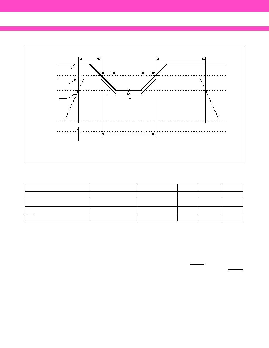
MB84VD23581FJ
-70
52
∑ Data Retention Timing
s
s
s
s
PIN CAPACITANCE
Note : Test conditions T
A
=
+
25
∞
C, f
=
1.0 MHz
s
s
s
s
HANDLING OF PACKAGE
Please handle this package carefully since the sides of package create acute angles.
s
s
s
s
CAUTION
∑
The high voltage (V
ID
) cannot apply to address pins and control pins except RESET. Exception is when
autoselect and sector group protect function are used, then the high voltage (V
ID
) can be applied to RESET.
∑
Without the high voltage (V
ID
) , sector group protection can be achieved by using "Extended Sector Group
Protection" command.
Parameter
Symbol
Test Setup
Typ
Max
Unit
Input Capacitance
C
IN
V
IN
= 0
11
14
pF
Output Capacitance
C
OUT
V
OUT
= 0
12
16
pF
Control Pin Capacitance
C
IN2
V
IN
= 0
14
16
pF
WP/ACC Pin Capacitance
C
IN3
V
IN
= 0
21.5
26
pF
V/
t
CE1r
t
DRR
Data Retention Mode
t
DRS
CE1r
=
CE2r >
V
CC
r-
0.2 V
or V
IH
* Min
V
CC
r
2.7 V
3.1 V
0.4 V
2.3 V
V
SS
V/
t
CE2r
Data bus must be in High-Z at data retention entry.
* : 2.0 V
V
IH
Vccr
+
0.3 V

MB84VD23581FJ
-70
53
s
s
s
s
ORDERING INFORMATION
MB84VD23581 FJ -70 PBS
DEVICE NUMBER/DESCRIPTION
64 Mega-bit (4 M
◊
16 bit) Dual Operation Flash Memory
3.0 V-only Read, Program, and Erase
32 Mega-bit (2 M
◊
16 bit) FCRAM
PACKAGE TYPE
PBS
=
65-ball FBGA
SPEED OPTION
See Product Selector Guide
Device Revision
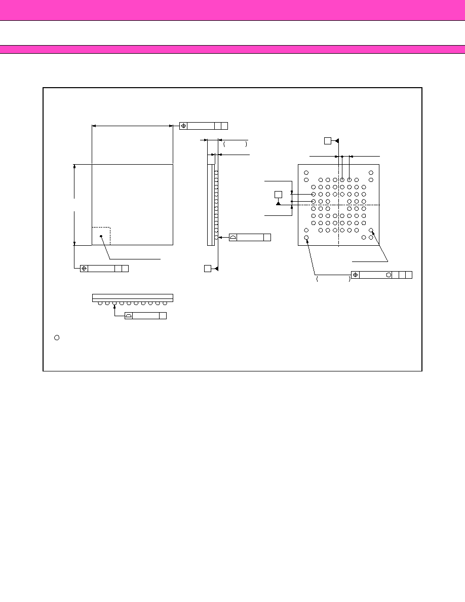
MB84VD23581FJ
-70
54
s
s
s
s
PACKAGE DIMENSION
65-ball plastic FBGA
(BGA-65P-M01)
Dimensions in mm (inches).
Note: The values in parentheses are reference values.
C
2001 FUJITSU LIMITED B65001S-c-1-2
9.00±0.10(.354±.004)
9.00±0.10
(.354±.004)
INDEX-MARK AREA
0.10(.004)
0.39±0.10
(.015±.004)
(Stand off)
.047
≠.004
+.006
≠0.10
+0.15
1.19
(Seated height)
A
B
C
D
E
F
G
H
J
K
1
2
3
4
5
6
7
8
9
10
65-
ÿ.018
≠.002
+.004
≠0.05
+0.10
65-
ÿ0.45
M
0.08(.003)
0.20(.008) S A
S
S
0.80(.031)
0.40(.016)
REF
REF
0.80(.031)
REF
REF
0.40(.016)
A
B
S A
S
0.10(.004)
B
S
0.20(.008)
B
INDEX BALL

MB84VD23581FJ
-70
FUJITSU LIMITED
All Rights Reserved.
The contents of this document are subject to change without notice.
Customers are advised to consult with FUJITSU sales
representatives before ordering.
The information, such as descriptions of function and application
circuit examples, in this document are presented solely for the
purpose of reference to show examples of operations and uses of
Fujitsu semiconductor device; Fujitsu does not warrant proper
operation of the device with respect to use based on such
information. When you develop equipment incorporating the
device based on such information, you must assume any
responsibility arising out of such use of the information. Fujitsu
assumes no liability for any damages whatsoever arising out of
the use of the information.
Any information in this document, including descriptions of
function and schematic diagrams, shall not be construed as license
of the use or exercise of any intellectual property right, such as
patent right or copyright, or any other right of Fujitsu or any third
party or does Fujitsu warrant non-infringement of any third-party's
intellectual property right or other right by using such information.
Fujitsu assumes no liability for any infringement of the intellectual
property rights or other rights of third parties which would result
from the use of information contained herein.
The products described in this document are designed, developed
and manufactured as contemplated for general use, including
without limitation, ordinary industrial use, general office use,
personal use, and household use, but are not designed, developed
and manufactured as contemplated (1) for use accompanying fatal
risks or dangers that, unless extremely high safety is secured, could
have a serious effect to the public, and could lead directly to death,
personal injury, severe physical damage or other loss (i.e., nuclear
reaction control in nuclear facility, aircraft flight control, air traffic
control, mass transport control, medical life support system, missile
launch control in weapon system), or (2) for use requiring
extremely high reliability (i.e., submersible repeater and artificial
satellite).
Please note that Fujitsu will not be liable against you and/or any
third party for any claims or damages arising in connection with
above-mentioned uses of the products.
Any semiconductor devices have an inherent chance of failure. You
must protect against injury, damage or loss from such failures by
incorporating safety design measures into your facility and
equipment such as redundancy, fire protection, and prevention of
over-current levels and other abnormal operating conditions.
If any products described in this document represent goods or
technologies subject to certain restrictions on export under the
Foreign Exchange and Foreign Trade Law of Japan, the prior
authorization by Japanese government will be required for export
of those products from Japan.
F0307
©
FUJITSU LIMITED Printed in Japan