 | –≠–ª–µ–∫—Ç—Ä–æ–Ω–Ω—ã–π –∫–æ–º–ø–æ–Ω–µ–Ω—Ç: S25FL004D | –°–∫–∞—á–∞—Ç—å:  PDF PDF  ZIP ZIP |

Publication Number S25FL004D_00 Revision A Amendment 0 Issue Date June 28, 2004
ADVANCE
INFORMATION
S25FL Family (Serial Peripheral Interface)
S25FL004D
4 Megabit CMOS 3.0 Volt Flash Memory
with 50 Mhz SPI Bus Interface
Distinctive Characteristics
ARCHITECTURAL ADVANTAGES
Single power supply operation
-- Full voltage range: 2.7 to 3.6 V read and program
operations
Memory Architecture
-- Eight sectors with 512 Kb each
Program
-- Page Program (up to 256 bytes) in 1.5 ms (typical)
-- Program cycles are on a page by page basis
Erase
-- 0.5 s typical sector erase time
-- 4 s typical bulk erase time
Endurance
-- 100,000 cycles per sector typical
Data Retention
-- 20 years typical
Device ID
-- Electronic signature
Process Technology
-- Manufactured on 0.25 µm process technology
Package Option
-- Industry Standard Pinouts
-- 8-pin SO (208mil) package
-- 8-contact WSON leadless package (6x5mm)
PERFORMANCE CHARACTERISTICS
Speed
-- 50 MHz clock rate (maximum)
Power Saving Standby Mode
-- Standby Mode 1 µA (typical)
Memory Protection Features
Memory Protection
-- W# pin works in conjunction with Status Register Bits
to protect specified memory areas
-- Status Register Block Protection bits (BP1, BP0) in
status register configure parts of memory as read-
only
SOFTWARE FEATURES
SPI Bus Compatible Serial Interface

2
S25FL Family (Serial Peripheral Interface) S25FL004D
S25FL004D_00A0 June 28, 2004
A d v a n c e I n f o r m a t i o n
General Description
The S25FL004D device is a 3.0 Volt (2.7 V to 3.6 V) single power supply Flash memory
device. S25FL004D consists of eight sectors, each with 512 Kb memory.
Data appears on SI input pin when inputting data into the memory and on the SO output
pin when outputting data from the memory. The devices are designed to be programmed
in-system with the standard system 3.0 Volt V
CC
supply.
The memory can be programmed 1 to 256 bytes at a time, using the Page Program in-
struction.
The memory supports Sector Erase and Bulk Erase instructions.
Each device requires only a 3.0 Volt power supply (2.7 V to 3.6 V) for both read and write
functions. Internally generated and regulated voltages are provided for the program op-
erations. This device does not require V
PP
supply.

June 28, 2004 S25FL004D_00A0
S25FL Family (Serial Peripheral Interface) S25FL004D
3
A d v a n c e I n f o r m a t i o n
Table of Contents
Block Diagram . . . . . . . . . . . . . . . . . . . . . . . . . . . . .4
Connection Diagrams . . . . . . . . . . . . . . . . . . . . . . .5
Input/Output Descriptions . . . . . . . . . . . . . . . . . . . 5
Logic Symbol . . . . . . . . . . . . . . . . . . . . . . . . . . . . . . 5
Ordering Information . . . . . . . . . . . . . . . . . . . . . . . .6
Signal Description . . . . . . . . . . . . . . . . . . . . . . . . . . .7
SPI Modes ...................................................................................................7
Figure 1. Bus Master and Memory Devices on the SPI Bus ....... 8
Figure 2. SPI Modes Supported............................................ 8
Operating Features . . . . . . . . . . . . . . . . . . . . . . . . .9
Page Programming .................................................................................. 9
Sector Erase, or Bulk Erase ................................................................. 9
Polling During a Write, Program, or Erase Cycle ........................ 9
Status Register ......................................................................................... 9
Protection Modes ..................................................................................10
Table 1. Protected Area Sizes (S25FL004D). .........................10
Hold Condition Modes ........................................................................10
Figure 3. Hold Condition Activation...................................... 11
Memory Organization . . . . . . . . . . . . . . . . . . . . . . 12
Table 2. Sector Address Table ≠ S25FL004D .........................12
Instructions . . . . . . . . . . . . . . . . . . . . . . . . . . . . . . . 13
Table 3. Instruction Set. ....................................................13
Write Enable (WREN) .........................................................................14
Figure 4. Write Enable (WREN) Instruction Sequence............. 14
Write Disable (WRDI) ........................................................................14
Figure 5. Write Disable (WRDI) Instruction Sequence ............ 14
Read Status Register (RDSR) ............................................................. 15
Figure 6. Read Status Register (RDSR)
Instruction Sequence ........................................................ 15
Figure 7. Status Register Format......................................... 15
Write Status Register (WRSR) .......................................................... 16
Figure 8. Write Status Register (WRSR)
Instruction Sequence ........................................................ 17
Table 4. Protection Modes ..................................................17
Read Data Bytes (READ) ....................................................................18
Figure 9. Read Data Bytes (READ) Instruction Sequence ........ 18
Read Data Bytes at Higher Speed (FAST_READ) .......................18
Figure 10. Read Data Bytes at Higher Speed
(FAST_READ) Instruction Sequence..................................... 19
Page Program (PP) ................................................................................. 19
Figure 11. Page Program (PP) Instruction Sequence .............. 20
Sector Erase (SE) ..................................................................................20
Figure 12. Sector Erase (SE) Instruction Sequence ................ 21
Bulk Erase (BE) ....................................................................................... 21
Figure 13. Bulk Erase (BE) Instruction Sequence................... 22
Deep Power Down (DP) ....................................................................22
Figure 14. Deep Power Down (DP) Instruction Sequence ........ 23
Release from Deep Power Down (RES) ....................................... 23
Figure 15. Release from Deep Power Down I
nstruction Sequence.......................................................... 24
Release from Deep Power Down and Read Electronic
Signature (RES) ......................................................................................24
Figure 16. Release from Deep Power Down and Read Electronic
Signature (RES) Instruction Sequence ................................. 25
Power-up and Power-down . . . . . . . . . . . . . . . . . . 26
Figure 17. Power-Up Timing ............................................... 27
Figure 18. Power-Down and Voltage Drop ............................ 27
Table 5. Power-Up Timing ................................................. 28
Initial Delivery State . . . . . . . . . . . . . . . . . . . . . . . 28
Maximum Rating . . . . . . . . . . . . . . . . . . . . . . . . . . 28
Absolute Maximum Ratings . . . . . . . . . . . . . . . . . 28
Operating Ranges . . . . . . . . . . . . . . . . . . . . . . . . . 28
DC Characteristics . . . . . . . . . . . . . . . . . . . . . . . . . 29
Table 6. DC Characteristics ............................................... 29
Test Conditions . . . . . . . . . . . . . . . . . . . . . . . . . . . 30
Figure 19. AC Measurements I/O Waveform ......................... 30
Table 7. Test Specifications ............................................... 30
Table 8. AC Characteristics ................................................ 31
Figure 20. SPI Mode 0 (0,0) Input Timing............................. 32
Figure 21. SPI Mode 0 (0,0) Output Timing .......................... 32
Figure 22. HOLD# Timing .................................................. 33
Figure 23. Write Protect Setup and Hold Timing during WRSR when
SRWD=1 ......................................................................... 33
Physical Dimensions . . . . . . . . . . . . . . . . . . . . . . . . 34
S08 wide--8-pin Plastic Small Outline 208mils Body Width
Package ................................................................................................... 34
8-Contact WSON (6mm x 5mm) Leadless Package .................35
Revision Summary . . . . . . . . . . . . . . . . . . . . . . . . . 36
4
S25FL Family (Serial Peripheral Interface) S25FL004D
S25FL004D_00A0 June 28, 2004
A d v a n c e I n f o r m a t i o n
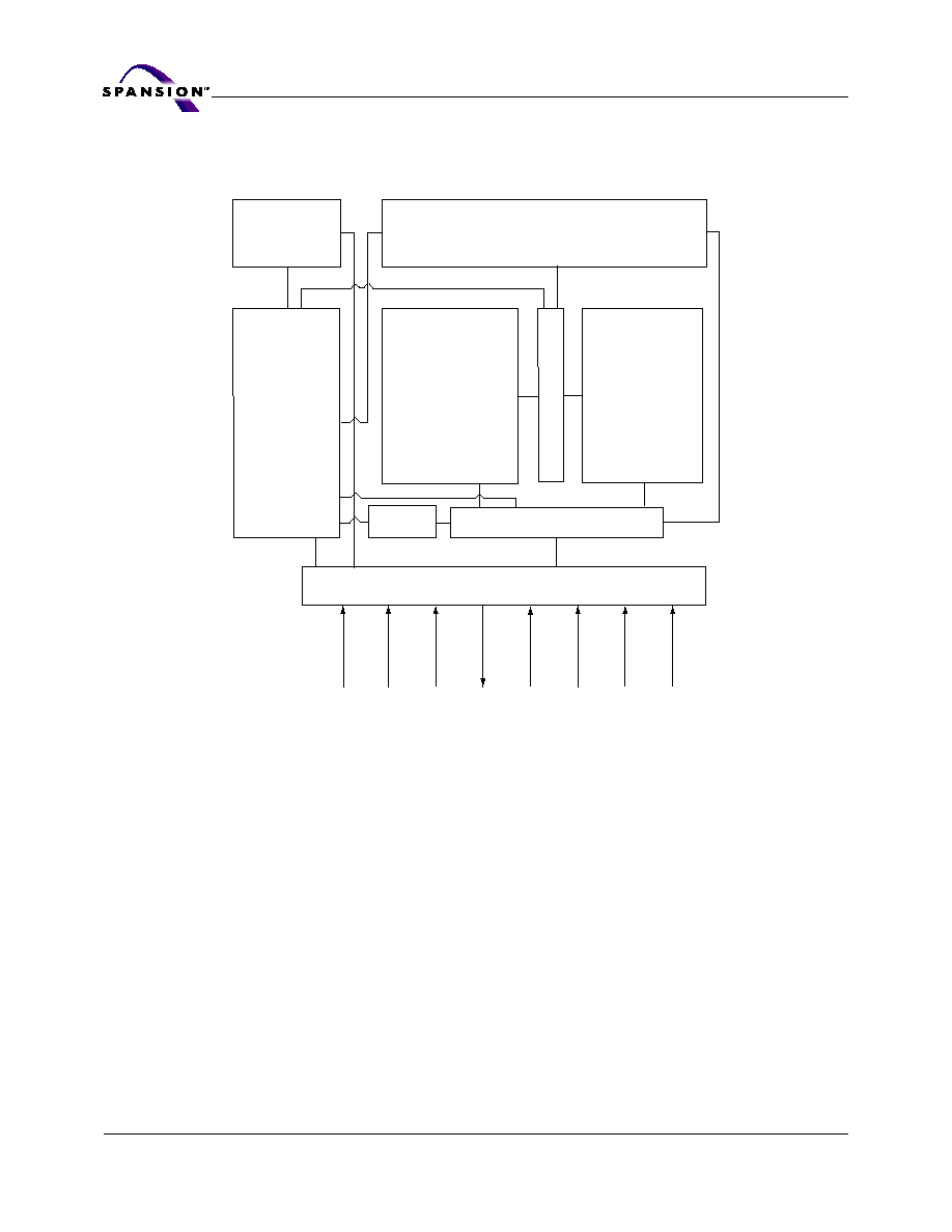
Block Diagram
SCK
SI
SO
GND
V
CC
W#
HOLD#
SRAM
PS
Logic
Array - L
Array - R
RD
DATA PATH
IO
X
D
E
C
CS#
June 28, 2004 S25FL004D_00A0
S25FL Family (Serial Peripheral Interface) S25FL004D
5
A d v a n c e I n f o r m a t i o n
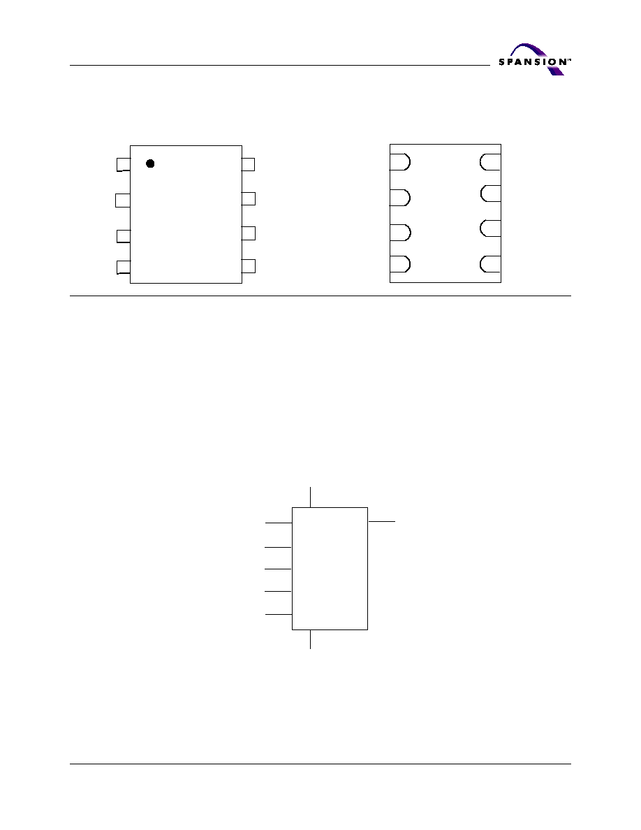
Connection Diagrams
Input/Output Descriptions
SCK
=
Serial Clock Input
SI
=
Serial Data Input
SO
=
Serial Data Output
CS#
=
Chip Select Input
W#
=
Write Protect Input
HOLD#
=
Hold Input
V
CC
=
Supply Voltage Input
GND
=
Ground Input
Logic Symbol
1
2
3
4
8
7
6
5
CS#
SO
W#
GND
SI
SCK
HOLD#
VCC
1
2
3
4
8
7
6
5
CS#
SO
W#
GND
SI
SCK
HOLD#
VCC
8-pin Plastic Small Outline Package (SO)
8-contact WSON Package
CS#
SO
W#
GND
SI
SCK
HOLD#
VCC
6
S25FL Family (Serial Peripheral Interface) S25FL004D
S25FL004D_00A0 June 28, 2004
A d v a n c e I n f o r m a t i o n
Ordering Information
The order number (Valid Combination) is formed by the following:
Notes:
1. Type 1 is standard. Specify other options as required.
2. Contact your local sales office for availability.
3. Package marking omits leading "S25" and speed, package, and leading digit of model number from ordering part
number.
4. If "Last Digit of Model Number" is 3, this signifies a S08-Wide body Lead (Pb)-free package. For example: FL004DI3.
If "Last Digit of Model Number" is 1, this signifies a S08-Wide body standard package. For example: FL004DI1.
Valid Combinations
Valid Combination configuration planned to be supported for this device. Note: Ordering
part number and package marking is pending final product introduction. Contact your sales
representative for further information.
S25FL
004
D
0L
M
A
I
01
I
PACKING TYPE
1
= Tube (standard) (Note 1)
3
= 13" Tape and Reel (Note 2)
MODEL NUMBER (Additional Ordering Options)
01
= S0-8 Wide (208mil) Package
TEMPERATURE RANGE
I = Industrial
(≠40
∞
C to +85
∞
C)
PACKAGE MATERIALS
A
= Standard
F
= Lead (Pb) -free (Note 2)
PACKAGE TYPE
M
= 8 pin Plastic Small Outline Package
N
= WSON (Note 2)
SPEED
0L
= 50 MHz
DEVICE TECHNOLOGY
D
= 0.25 µm process technology
DENSITY
004
= 4 Mb
DEVICE FAMILY
S25FL
Spansion
TM
Memory 3.0 Volt-only, Serial Peripheral Interface (SPI) Flash Memory
S25FL Valid Combinations
Base
Ordering
Part Number
Speed
Option
Package &
Temperature
Model
Number
Packing
Type
Package Marking
S25FL004D
0L
MAI, MFI, NFI
01
1, 3
(Note 1)
FL004D + (Temp) + (Last Digit of Model Number)
(Note 4)

June 28, 2004 S25FL004D_00A0
S25FL Family (Serial Peripheral Interface) S25FL004D
7
A d v a n c e I n f o r m a t i o n
Signal Description
Signal Data Output (SO): This output signal is used to transfer data serially out
of the device. Data is shifted out on the falling edge of Serial Clock (SCK).
Serial Data Input (SI): This input signal is used to transfer data serially into
the device. It receives instructions, addresses, and the data to be programmed.
Values are latched on the rising edge of Serial Clock (SCK).
Serial Clock (SCK): This input signal provides the timing of the serial interface.
Instructions, addresses, and data present at the Serial Data input (SI) are latched
on the rising edge of Serial Clock (SCK). Data on Serial Data Output (SO) changes
after the falling edge of Serial Clock (SCK).
Chip Select (CS#): When this input signal is High, the device is deselected and
Serial Data Output (SO) is at high impedance. Unless an internal Program, Erase
or Write Status Register cycle is in progress, the device will be in Standby mode.
Driving Chip Select (CS#) Low enables the device, placing it in the active power
mode.
After Power-up, a falling edge on Chip Select (CS#) is required prior to the start
of any instruction.
Hold (HOLD#): The Hold (HOLD#) signal is used to pause any serial communi-
cations with the device without deselecting the device.
During the Hold instruction, the Serial Data Output (SO) is high impedance, and
Serial Data Input (SI) and Serial Clock (SCK) are Don't Care.
To start the Hold condition, the device must be selected, with Chip Select (CS#)
driven Low.
Write Protect (W#): The main purpose of this input signal is to freeze the size
of the area of memory that is protected against program or erase instructions (as
specified by the values in the BP1 and BP0 bits of the Status Register).
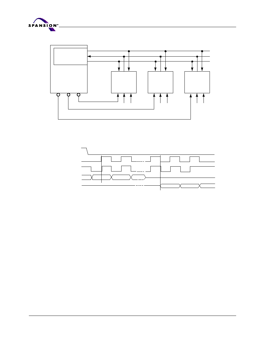
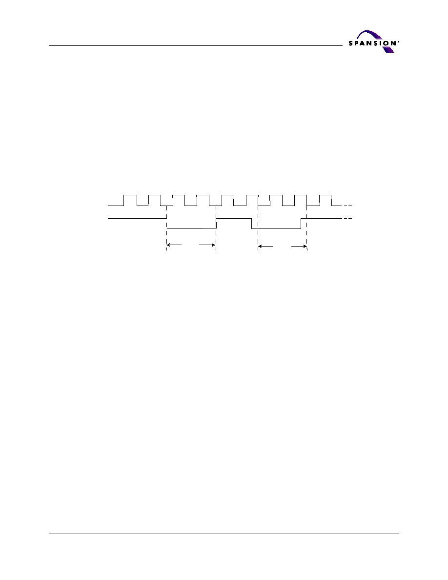
SPI Modes
These devices can be driven by a microcontroller with its SPI peripheral running
in either of the two following modes:
CPOL = 0, CPHA = 0
CPOL = 1, CPHA = 1
For these two modes, input data is latched in on the rising edge of Serial Clock
(SCK), and output data is available from the falling edge of Serial Clock (SCK).
The difference between the two modes, as shown in
Figure 2
, is the clock polarity
when the bus master is in Standby and not transferring data:
SCK remains at 0 for (CPOL = 0, CPHA = 0)
SCK remains at 1 for (CPOL = 1, CPHA = 1)
8
S25FL Family (Serial Peripheral Interface) S25FL004D
S25FL004D_00A0 June 28, 2004
A d v a n c e I n f o r m a t i o n
Figure 1. Bus Master and Memory Devices on the SPI Bus
Note: The Write Protect (W#) and Hold (HOLD#) signals should be driven, High or Low as appropriate.
Figure 2. SPI Modes Supported
SPI Interface with
(CPOL, CPHA) =
(0, 0) or (1, 1)
Bus Master
CS3
CS2
CS1
SPI Memory
Device
SPI Memory
Device
SPI Memory
Device
CS#
W# HOLD#
CS#
W# HOLD#
CS#
W# HOLD#
SCK SO SI
SCK SO SI
SCK SO SI
SO
SI
SCK
MSB
MSB
SCK
SCK
SI
SO
CPHA
CPOL
0
0
1
1
CS#

June 28, 2004 S25FL004D_00A0
S25FL Family (Serial Peripheral Interface) S25FL004D
9
A d v a n c e I n f o r m a t i o n
Operating Features
All data into and out of the device is shifted in 8-bit chunks.
Page Programming
To program one data byte, two instructions are required: Write Enable (WREN),
which is one byte, and a Page Program (PP) sequence, which consists of four
bytes plus data. This is followed by the internal Program cycle. To spread this
overhead, the Page Program (PP) instruction allows up to 256 bytes to be pro-
grammed at a time (changing bits from 1 to 0), provided that they lie in
consecutive addresses on the same page of memory.
Sector Erase, or Bulk Erase
The Page Program (PP) instruction allows bits to be programmed from 1 to 0. Be-
fore this can be applied, the bytes of the memory need to be first erased to all
1's (FFh) before any programming. This can be achieved in two ways: 1) a sector
at a time using the Sector Erase (SE) instruction, or 2) throughout the entire
memory, using the Bulk Erase (BE) instruction.
Polling During a Write, Program, or Erase Cycle
A further improvement in the time to Write Status Register (WRSR), Program (PP)
or Erase (SE or BE) can be achieved by not waiting for the worst-case delay. The
Write in Progress (WIP) bit is provided in the Status Register so that the applica-
tion program can monitor its value, polling it to establish when the previous Write
cycle, Program cycle, or Erase cycle is complete.
Active Power and Standby Power Modes
When Chip Select (CS#) is Low, the device is enabled, and in the Active Power
mode. When Chip Select (CS#) is High, the device is disabled, but could remain
in the Active Power mode until all internal cycles have completed (Program,
Erase, Write Status Register). The device then goes into the Standby Power
mode. The device consumption drops to I
SB
. This can be used as an extra Deep
Power Down on mechanism, when the device is not in active use, to protect the
device from inadvertent Write, Program, or Erase instructions.
Status Register
The Status Register contains a number of status and control bits, as shown in
Fig-
ure 7
, that can be read or set (as appropriate) by specific instructions
WIP bit: The Write In Progress (WIP) bit indicates whether the memory is
busy with a Write Status Register, Program or Erase cycle.
WEL bit: The Write Enable Latch (WEL) bit indicates the status of the internal
Write Enable Latch.
BP2, BP1, BP0 bits: The Block Protect (BP2, BP1, BP0) bits are non-volatile.
They define the size of the area to be software protected against Program and
Erase instructions.
SRWD bit: The Status Register Write Disable (SRWD) bit is operated in con-
junction with the Write Protect (W#) signal. The Status Register Write Disable
(SRWD) bit and Write Protect (W#) signal allow the device to be put in the
Hardware Protected mode. In this mode, the non-volatile bits of the Status
Register (SRWD, BP2, BP1, BP0) become read-only bits.

10
S25FL Family (Serial Peripheral Interface) S25FL004D
S25FL004D_00A0 June 28, 2004
A d v a n c e I n f o r m a t i o n
Protection Modes
The SPI memory device boasts the following data protection mechanisms:
All instructions that modify data must be preceded by a Write Enable (WREN)
instruction to set the Write Enable Latch (WEL) bit. This bit is returned to its
reset state by the following events:
-- Power-up
-- Write Disable (WRDI) instruction completion
-- Write Status Register (WRSR) instruction completion
-- Page Program (PP) instruction completion
-- Sector Erase (SE) instruction completion
-- Bulk Erase (BE) instruction completion
The Block Protect (BP2, BP1, BP0) bits allow part of the memory to be con-
figured as read-only. This is the Software Protected Mode (SPM).
The Write Protect (W#) signal works in cooperation with the Status Register
Write Disable (SRWD) bit to enable write-protection. This is the Hardware
Protected Mode (HPM).
Program, Erase and Write Status Register instructions are checked to verify
that they consist of a number of clock pulses that is a multiple of eight, before
they are accepted for execution.
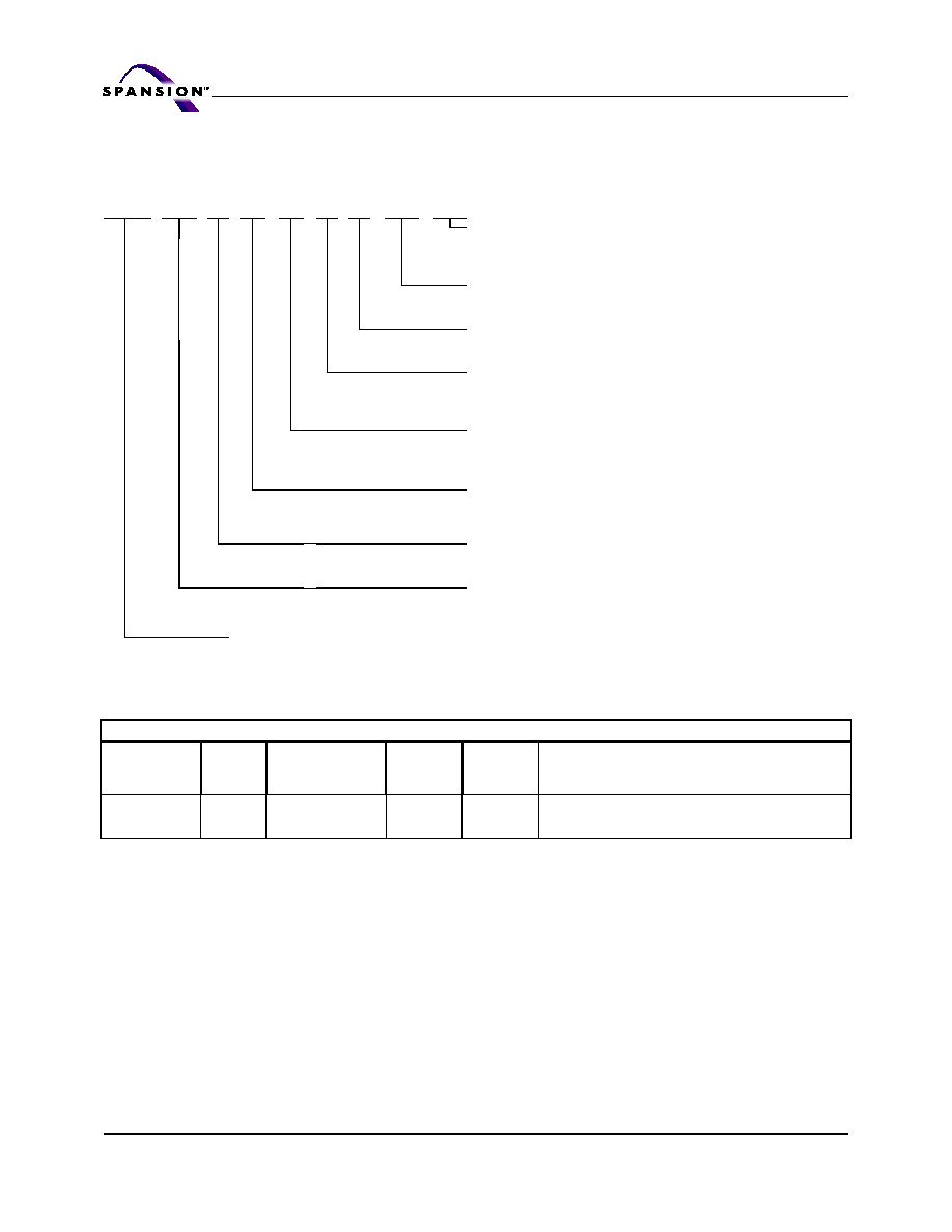
Table 1. Protected Area Sizes (S25FL004D).
Hold Condition Modes
The Hold (HOLD#) signal is used to pause any serial communications with the
device without resetting the clocking sequence. Hold (HOLD#) signal gates the
clock input to the device. However, taking this signal Low does not terminate any
Write Status Register, Program or Erase Cycle that is currently in progress.
To enter the Hold condition, the device must be selected, with Chip Select (CS#)
Low. The Hold condition starts on the falling edge of the Hold (HOLD#) signal,
provided that this coincides with Serial Clock (SCK) being Low (as shown in
Figure
3
).
The Hold condition ends on the rising edge of the Hold (HOLD#) signal, provided
that this coincides with Serial Clock (SCK) being Low.
Protected
Memory
Area
(Top Level)
Status Register Content
Memory Content
BP2 Bit
BP1 Bit
BP0
Protected Area
Unprotected Area
0
0
0
0
none
00000≠7FFFF
1/8
0
0
1
70000≠7FFFF
00000≠6FFFF
1/4
0
1
0
60000≠7FFFF
00000≠5FFFF
1/2
0
1
1
40000≠7FFFF
00000≠3FFFF
All
1
0
0
00000-7FFFF
none
All
1
0
1
00000-7FFFF
none
All
1
1
0
00000-7FFFF
none
All
1
1
1
00000-7FFFF
none
June 28, 2004 S25FL004D_00A0
S25FL Family (Serial Peripheral Interface) S25FL004D
11
A d v a n c e I n f o r m a t i o n
If the falling edge does not coincide with Serial Clock (SCK) being Low, the Hold
condition starts after Serial Clock (SCK) next goes Low. Similarly, if the rising
edge does not coincide with Serial Clock (SCK) being Low, the Hold condition ends
after Serial Clock (SCK) next goes Low (
Figure 3
). During the Hold condition, the
Serial Data Output (SO) is high impedance, and Serial Data Input (SI) and Serial
Clock (SCK) are Don't Care.
Normally, the device remains selected, with Chip Select (CS#) driven Low, for the
entire duration of the Hold condition. This ensures that the state of the internal
logic remains unchanged from the moment of entering the Hold condition.
If Chip Select (CS#) goes High while the device is in the Hold condition, this has
the effect of resetting the internal logic of the device. To restart communication
with the device, it is necessary to drive Hold (HOLD#) High, and then to drive
Chip Select (CS#) Low. This prevents the device from going back to the Hold
condition.
Figure 3. Hold Condition Activation
SCK
HOLD#
Hold
Condition
(standard use)
Hold
Condition
(non-standard use)
12
S25FL Family (Serial Peripheral Interface) S25FL004D
S25FL004D_00A0 June 28, 2004
A d v a n c e I n f o r m a t i o n
Memory Organization
The memory is organized as:
S25FL004D: Eight sectors of 512 Kbit each
Each page can be individually programmed (bits are programmed from 1 to
0).
The device is Sector or Bulk erasable (bits are erased from 0 to 1).
Table 2. Sector Address Table ≠ S25FL004D
Sector
Address Range
SA7
70000h
7FFFFh
SA6
60000h
6FFFFh
SA5
50000h
5FFFFh
SA4
40000h
4FFFFh
SA3
30000h
3FFFFh
SA2
20000h
2FFFFh
SA1
10000h
1FFFFh
SA0
00000h
0FFFFh
June 28, 2004 S25FL004D_00A0
S25FL Family (Serial Peripheral Interface) S25FL004D
13
A d v a n c e I n f o r m a t i o n
Instructions
All instructions, addresses, and data are shifted in and out of the device, starting
with the most significant bit. Serial Data Input (SI) is sampled on the first rising
edge of Serial Clock (SCK) after Chip Select (CS#) is driven Low. Then, the one-
byte instruction code must be shifted in to the device, most significant bit first,
on Serial Data Input (SI), each bit being latched on the rising edges of Serial
Clock (SCK). The instruction set is listed in Table
3
.
Every instruction sequence starts with a one-byte instruction code. Depending on
the instruction, this might be followed by address bytes, or by data bytes, or by
both or none. Chip Select (CS#) must be driven High after the last bit of the in-
struction sequence has been shifted in.
In the case of a Read Data Bytes (READ), Read Status Register (RDSR), Fast Read
(FAST_READ) or Release from Deep Power Down and Read Electronic Signature
(RES) instruction, the shifted-in instruction sequence is followed by a data-out
sequence. Chip Select (CS#) can be driven High after any bit of the data-out se-
quence is being shifted out to terminate the transaction.
In the case of a Page Program (PP), Sector Erase (SE), Bulk Erase (BE), Write
Status Register (WRSR), Write Enable (WREN), or Write Disable (WRDI) instruc-
tion, Chip Select (CS#) must be driven High exactly at a byte boundary,
otherwise the instruction is rejected, and is not executed. That is, Chip Select
(CS#) must driven High when the number of clock pulses after Chip Select (CS#)
being driven Low is an exact multiple of eight.
All attempts to access the memory array during a Write Status Register cycle,
Program cycle or Erase cycle are ignored, and the internal Write Status Register
cycle, Program cycle or Erase cycle continues unaffected
Table 3. Instruction Set.
Instruction
Description
One-Byte Instruction
Code
Address
Bytes
Dummy
Byte
Data Bytes
Status Register Operations
WREN
Write Enable
06H (0000 0110)
0
0
0
WRDI
Write Disable
04H (0000 0100)
0
0
0
RDSR
Read from Status Register
05H (0000 0101)
0
0
1 to Infinity
WRSR
Write to Status Register
01H (0000 0001)
0
0
1
Read Operations
READ
Read Data Bytes
03H (0000 0011)
3
0
1 to Infinity
FAST_READ
Read Data Bytes at Higher Speed
0BH (0000 1011)
3
1
1 to Infinity
Erase Operations
SE
Sector Erase
D8H (1101 1000)
3
0
0
BE
Bulk (Chip) Erase
C7H (1100 0111)
0
0
0
Program Operations
PP
Page Program
02H (0000 0010)
3
0
1 to 256
Deep Power Down Savings Mode Operations
DP
Deep Power Down
B9H (1011 1001)
0
0
0
RES
Release from Deep Power Down
ABH (1010 1011)
0
0
0
Release from Deep Power Down and
Read Electronic Signature
ABH (1010 1011)
0
3
1 to Infinity
14
S25FL Family (Serial Peripheral Interface) S25FL004D
S25FL004D_00A0 June 28, 2004
A d v a n c e I n f o r m a t i o n
Write Enable (WREN)
The Write Enable (WREN) instruction (
Figure 4
) sets the Write Enable Latch (WEL)
bit. The Write Enable Latch (WEL) bit must be set prior to every Page Program
(PP), Erase (SE or BE) and Write Status Register (WRSR) instruction. The Write
Enable (WREN) instruction is entered by driving Chip Select (CS#) Low, sending
the instruction code, and then driving Chip Select (CS#) High.
Figure 4. Write Enable (WREN) Instruction Sequence
Write Disable (WRDI)
The Write Disable (WRDI) instruction (
Figure 5
) resets the Write Enable Latch
(WEL) bit. The Write Disable (WRDI) instruction is entered by driving Chip Select
(CS#) Low, sending the instruction code, and then driving Chip Select (CS#)
High.
The Write Enable Latch (WEL) bit is reset under the following conditions:
Power-up
Write Disable (WRDI) instruction completion
Write Status Register (WRSR) instruction completion
Page Program (PP) instruction completion
Sector Erase (SE) instruction completion
Bulk Erase (BE) instruction completion
Figure 5. Write Disable (WRDI) Instruction Sequence
CS#
SCK
SI
SO
High Impedance
Instruction
0 1
2 3
4 5 6 7
0 1 2 3 4 5 6 7
SCK
SI
SO
High Impedance
Instruction
CS#

June 28, 2004 S25FL004D_00A0
S25FL Family (Serial Peripheral Interface) S25FL004D
15
A d v a n c e I n f o r m a t i o n
Read Status Register (RDSR)
The Read Status Register (RDSR) instruction allows the Status Register to be
read. The Status Register may be read at any time, even while a Program, Erase,
or Write Status Register cycle is in progress. When one of these cycles is in
progress, it is recommended to check the Write In Progress (WIP) bit before
sending a new instruction to the device. It is also possible to read the Status Reg-
ister continuously, as shown in
Figure 6
.
Figure 6. Read Status Register (RDSR) Instruction Sequence
Figure 7. Status Register Format
The status and control bits of the Status Register are as follows:
SRWD bit: The Status Register Write Disable (SRWD) bit is operated in conjunc-
tion with the Write Protect (W#) signal. The Status Register Write Disable
(SRWD) bit and Write Protect (W#) signal allow the device to be put in the Hard-
ware Protected mode (when the Status Register Write Disable (SRWD) bit is set
to 1, and Write Protect (W#) is driven Low). In this mode, the non-volatile bits
of the Status Register (SRWD, BP2, BP1, BP0) become read-only bits and the
Write Status Register (WRSR) instruction is no longer accepted for execution.
BP2, BP1, BP0 bits: The Block Protect (BP2, BP1, BP0) bits are non-volatile.
They define the size of the area to be software protected against Program and
Erase instructions. These bits are written with the Write Status Register (WRSR)
instruction. When one or both of the Block Protect (BP2, BP1, BP0) bits is set to
1, the relevant memory area (as defined in Table
1
) becomes protected against
Page Program (PP), and Sector Erase (SE) instructions. The Block Protect (BP2,
BP1, BP0) bits can be written provided that the Hardware Protected mode has not
Instruction
High Impedance
MSB
MSB
Status Register Out
Status Register Out
0
15
14
13
12
11
10
9
8
7
6
5
4
3
2
1
7 6
5 4 3 2 1 0
7 6 5 4 3 2 1 0 7
SO
SI
SCK
CS#
Status Register
Write Disable
Block Protect Bits
Write Enable Latch Bit
Write In Progress Bit
SRWD
0
0
BP2
BP1
BP0
WEL
WIP
b7
b0

16
S25FL Family (Serial Peripheral Interface) S25FL004D
S25FL004D_00A0 June 28, 2004
A d v a n c e I n f o r m a t i o n
been set. The Bulk Erase (BE) instruction is executed if, and only if, all Block Pro-
tect (BP2, BP1, BP0) bits are 0.
WEL bit: The Write Enable Latch (WEL) bit indicates the status of the internal
Write Enable Latch. When set to 1, the internal Write Enable Latch is set; when
set to 0, the internal Write Enable Latch is reset and no Write Status Register, Pro-
gram or Erase instruction is accepted.
WIP bit: The Write In Progress (WIP) bit indicates whether the memory is busy
with a Write Status Register, Program or Erase cycle. This bit is a read only bit
and is read by executing a RDSR instruction. If this bit is 1, such a cycle is in
progress, if it is 0, no such cycle is in progress.
Write Status Register (WRSR)
The Write Status Register (WRSR) instruction allows new values to be written to
the Status Register. Before it can be accepted, a Write Enable (WREN) instruction
must previously have been executed. After the Write Enable (WREN) instruction
has been decoded and executed, the device sets the Write Enable Latch (WEL).
The Write Status Register (WRSR) instruction is entered by driving Chip Select
(CS#) Low, followed by the instruction code and the data byte on Serial Data
Input (SI).
The instruction sequence is shown in
Figure 8
.
The Write Status Register (WRSR) instruction has no effect on bits b6, b5, b1 and
b0 of the Status Register. Bits b6, b5 are always read as 0.
Chip Select (CS#) must be driven High after the eighth bit of the data byte has
been latched in. If not, the Write Status Register (WRSR) instruction is not exe-
cuted. As soon as Chip Select (CS#) is driven High, the self-timed Write Status
Register cycle (whose duration is t
W
) is initiated. While the Write Status Register
cycle is in progress, the Status Register may still be read to check the value of
the Write In Progress (WIP) bit. The Write In Progress (WIP) bit is 1 during the
self-timed Write Status Register cycle, and is 0 when it is completed. At some un-
specified time before the cycle is completed, the Write Enable Latch (WEL) is
reset.
The Write Status Register (WRSR) instruction allows the user to change the val-
ues of the Block Protect (BP2, BP1, BP0) bits, to define the size of the area that
is to be treated as read-only, as defined in Table
1
. The Write Status Register
(WRSR) instruction also allows the user to set or reset the Status Register Write
Disable (SRWD) bit in accordance with the Write Protect (W#) signal. The Status
Register Write Disable (SRWD) bit and Write Protect (W#) signal allow the device
to be put in the Hardware Protected Mode (HPM). The Write Status Register
(WRSR) instruction cannot be executed once the Hardware Protected Mode (HPM)
is entered.

June 28, 2004 S25FL004D_00A0
S25FL Family (Serial Peripheral Interface) S25FL004D
17
A d v a n c e I n f o r m a t i o n
Figure 8. Write Status Register (WRSR) Instruction Sequence
Table 4. Protection Modes
5. As defined by the values in the Block Protect (BP2, BP1, BP0) bits of the Status Register, as shown in Table
1
.
The protection features of the device are summarized in Table
4
.
When the Status Register Write Disable (SRWD) bit of the Status Register is 0 (its
initial delivery state), it is possible to write to the Status Register provided that
the Write Enable Latch (WEL) bit has previously been set by a Write Enable
(WREN) instruction, regardless of the whether Write Protect (W#) is driven High
or Low.
When the Status Register Write Disable (SRWD) bit of the Status Register is set
to 1, two cases need to be considered, depending on the state of Write Protect
(W#):
If Write Protect (W#) is driven High, it is possible to write to the Status Reg-
ister provided that the Write Enable Latch (WEL) bit has previously been set
by a Write Enable (WREN) instruction.
If Write Protect (W#) is driven Low, it is not possible to write to the Status
Register even if the Write Enable Latch (WEL) bit has previously been set by
a Write Enable (WREN) instruction. (Attempts to write to the Status Register
are rejected, and are not accepted for execution). As a consequence, all the
data bytes in the memory area that are software protected (SPM) by the
Block Protect (BP2, BP1, BP0) bits of the Status Register, are also hardware
protected against data modification.
Regardless of the order of the two events, the Hardware Protected Mode (HPM)
can be entered:
by setting the Status Register Write Disable (SRWD) bit after driving Write
Protect (W#) Low
W# Signal SRWD Bit
Mode
Write Protection of the Status
Register
Protected Area
(Note 1)
Unprotected Area
(Note 1)
1
1
Software
Protected
(SPM)
Status Register is Writeable (if the
WREN instruction has set the WEL
bit)
The values in the SRWD, BP2, BP1
and BP0 bits can be changed
Protected against Page
Program and Erase
(SE, BE)
Ready to accept Page
Program and Sector
Erase Instructions
1
0
0
0
0
1
Hardware
Protected
(HPM)
Status Register is Hardware write
protected
The values in the SRWD, BP2, BP1
and BP0 bits cannot be changed
Protected against Page
Program and Erase
(SE, BE)
Ready to accept Page
Program and Sector
Erase Instructions
High Impedance
MSB
Instruction
Status
Register In
CS#
SCK
SI
SO
0 1 2 3 4 5 6 7 8 9 10 11 12 13 14 15

18
S25FL Family (Serial Peripheral Interface) S25FL004D
S25FL004D_00A0 June 28, 2004
A d v a n c e I n f o r m a t i o n
or by driving Write Protect (W#) Low after setting the Status Register Write
Disable (SRWD) bit.
The only way to exit the Hardware Protected Mode (HPM) once entered is to pull
Write Protect (W#) High.
If Write Protect (W#) is permanently tied High, the Hardware Protected Mode
(HPM) can never be activated, and only the Software Protected Mode (SPM),
using the Block Protect (BP2, BP1, BP0) bits of the Status Register, can be used.
Read Data Bytes (READ)
The READ instruction reads the memory at the specified SCK frequency (f
SCK
)
with a maximum speed of 33 MHz.
The device is first selected by driving Chip Select (CS#) Low. The instruction code
for the Read Data Bytes (READ) instruction is followed by a 3-byte address (A23-
A0), each bit being latched-in during the rising edge of Serial Clock (SCK). Then
the memory contents, at that address, are shifted out on Serial Data Output
(SO), each bit being shifted out, at a frequency f
SCK
, during the falling edge of
Serial Clock (SCK).
The instruction sequence is shown in
Figure 9
. The first byte addressed can be at
any location. The address is automatically incremented to the next higher ad-
dress after each byte of data is shifted out. The whole memory can, therefore, be
read with a single Read Data Bytes (READ) instruction. When the highest address
is reached, the address counter rolls over to 00000h, allowing the read sequence
to be continued indefinitely.
The Read Data Bytes (READ) instruction is terminated by driving Chip Select
(CS#) High. Chip Select (CS#) can be driven High at any time during data output.
Any Read Data Bytes (READ) instruction, while a Program, Erase, or Write cycle
is in progress, is rejected without having any effect on the cycle that is in
progress.
Figure 9. Read Data Bytes (READ) Instruction Sequence
Read Data Bytes at Higher Speed (FAST_READ)
The FAST_READ instruction reads the memory at the specified SCK frequency
(f
SCK
) with a maximum speed of 50 MHz. The device is first selected by driving
Chip Select (CS#) Low. The instruction code for (FAST_READ) instruction is fol-
lowed by a 3-byte address (A23-A0) and a dummy byte, each bit being latched-
in during the rising edge of Serial Clock (SCK). Then the memory contents, at that
Instruction
24-Bit Address
High Impedance
MSB
MSB
Data Out 1
Data Out 2
0
31 32 33 34 35 36 37 38 39
30
23
28
10
9
8
7
6
5
4
3
2
1
7 6 5
23 22 21
4
3 2
1 0
3
2
1 0 7
SO
SI
SCK
CS#

June 28, 2004 S25FL004D_00A0
S25FL Family (Serial Peripheral Interface) S25FL004D
19
A d v a n c e I n f o r m a t i o n
address, are shifted out on Serial Data Output (SO), each bit being shifted out,
at a maximum frequency F
SCK
, during the falling edge of Serial Clock (SCK).
The instruction sequence is shown in
Figure 10
. The first byte addressed can be
at any location. The address is automatically incremented to the next higher ad-
dress after each byte of data is shifted out. The whole memory can, therefore, be
read with a single (FAST_READ) instruction. When the highest address is
reached, the address counter rolls over to 00000h, allowing the read sequence to
be continued indefinitely.
The (FAST_READ) instruction is terminated by driving Chip Select (CS#) High.
Chip Select (CS#) can be driven High at any time during data output. Any
(FAST_READ) instruction, while an Erase, Program or Write cycle is in progress,
is rejected without having any effects on the cycle that is in progress.
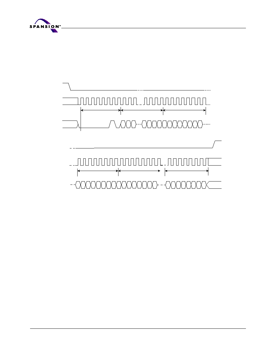
Figure 10. Read Data Bytes at Higher Speed (FAST_READ) Instruction Sequence
Page Program (PP)
The Page Program (PP) instruction allows bytes to be programmed in the memory
(changing bits from 1 to 0). Before it can be accepted, a Write Enable (WREN)
instruction must previously have been executed. After the Write Enable (WREN)
instruction has been decoded, the device sets the Write Enable Latch (WEL).
The Page Program (PP) instruction is entered by driving Chip Select (CS#) Low,
followed by the instruction code, three address bytes and at least one data byte
on Serial Data Input (SI). Chip Select (CS#) must be driven Low for the entire
duration of the sequence.
The instruction sequence is shown in
Figure 11
.
If more than 256 bytes are sent to the device, the addressing will wrap to the
beginning of the same page, previously latched data are discarded and the last
256 data bytes are guaranteed to be programmed correctly within the same
page. If fewer than 256 Data bytes are sent to device, they are correctly pro-
grammed at the requested addresses without having any effects on the other
bytes of the same page.
Chip Select (CS#) must be driven High after the eighth bit of the last data byte
has been latched in, otherwise the Page Program (PP) instruction is not executed.
As soon as Chip Select (CS#) is driven High, the self-timed Page Program cycle
(whose duration is t
PP
) is initiated. While the Page Program cycle is in progress,
CS#
SCK
SI
SO
Instruction
24-Bit
Address
Dummy Byte
High Impedance
DATA OUT 1
DATA OUT 2
MSB
MSB
0
1
2
3
4
5
6
7
8
9
10
28 29 30
31 32 33
34 35 36 37 38
39
40 41
42 43 44 45
46
47
23 22 21
3
2
1
0
7
6
5
4
3
2
1
0
7
6
5
4
3
2
1
0
7
20
S25FL Family (Serial Peripheral Interface) S25FL004D
S25FL004D_00A0 June 28, 2004
A d v a n c e I n f o r m a t i o n
the Status Register may be read to check the value of the Write In Progress (WIP)
bit. The Write In Progress (WIP) bit is 1 during the self-timed Page Program cycle,
and is 0 when it is completed. At some unspecified time before the cycle is com-
pleted, the Write Enable Latch (WEL) bit is reset.
A Page Program (PP) instruction applied to a page that is protected by the Block
Protect (BP2, BP1, BP0) bits (see Table
1
) is not executed.
Figure 11. Page Program (PP) Instruction Sequence
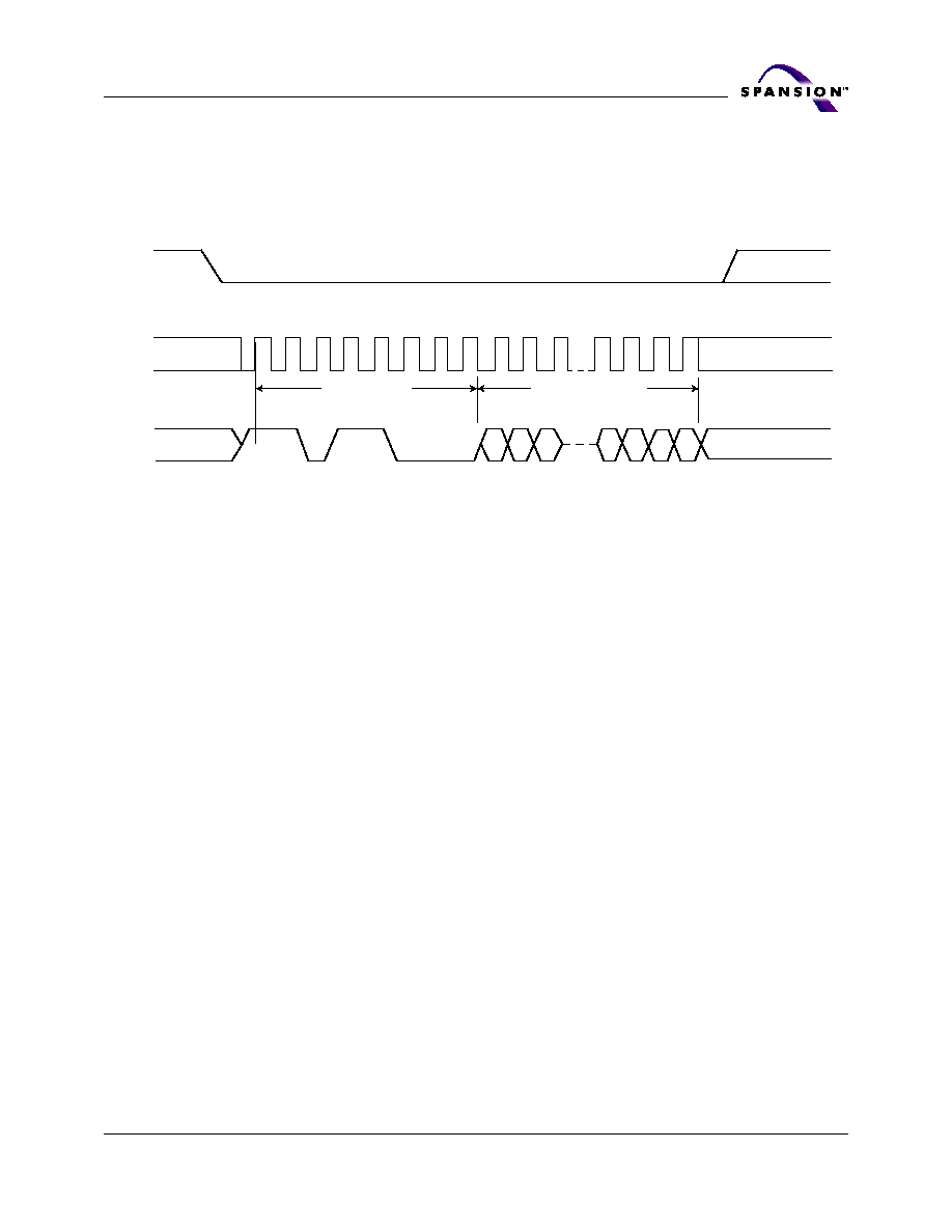
Sector Erase (SE)
The Sector Erase (SE) instruction sets to 1 (FFh) all bits inside the chosen sector.
Before it can be accepted, a Write Enable (WREN) instruction must previously
have been executed. After the Write Enable (WREN) instruction has been de-
coded, the device sets the Write Enable Latch (WEL).
The Sector Erase (SE) instruction is entered by driving Chip Select (CS#) Low,
followed by the instruction code, and three address bytes on Serial Data Input
(SI). Any address inside the Sector (see Table
1
) is a valid address for the Sector
Erase (SE) instruction. Chip Select (CS#) must be driven Low for the entire du-
ration of the sequence.
The instruction sequence is shown in
Figure 12
.
Chip Select (CS#) must be driven High after the eighth bit of the last address byte
has been latched in, otherwise the Sector Erase (SE) instruction is not executed.
As soon as Chip Select (CS#) is driven High, the self-timed Sector Erase cycle
(whose duration is tSE) is initiated. While the Sector Erase cycle is in progress,
the Status Register may be read to check the value of the Write In Progress (WIP)
bit. The Write In Progress (WIP) bit is 1 during the self-timed Sector Erase cycle,
0
34
33
32
31
30
29
28
10
9
8
7
6
5
4
3
2
1
35 36 37 38 39
46
45
44
43
42
41
40
47 48 49 50 51 52 53 54 55
2073
2072
2076
2075
2074
2079
2078
2077
23 22 21
3
2
1
0
7
6
5
4
3
2
1
0
Data Byte 1
24-Bit Address
Instruction
Data Byte 2
Data Byte 3
Data Byte 256
MSB
MSB
MSB
MSB
MSB
SCK
SI
SCK
SI
7
6
5
4
3
2
1
0
7
6
5
4
3
2
1
0
7
6
5
4
3
2
1
0
CS#
CS#
June 28, 2004 S25FL004D_00A0
S25FL Family (Serial Peripheral Interface) S25FL004D
21
A d v a n c e I n f o r m a t i o n
and is 0 when it is completed. At some unspecified time before the cycle is com-
pleted, the Write Enable Latch (WEL) bit is reset.
A Sector Erase (SE) instruction applied to any memory area that is protected by
the Block Protect (BP2, BP1, BP0) bits (see Table
1
) is not executed.
Figure 12. Sector Erase (SE) Instruction Sequence
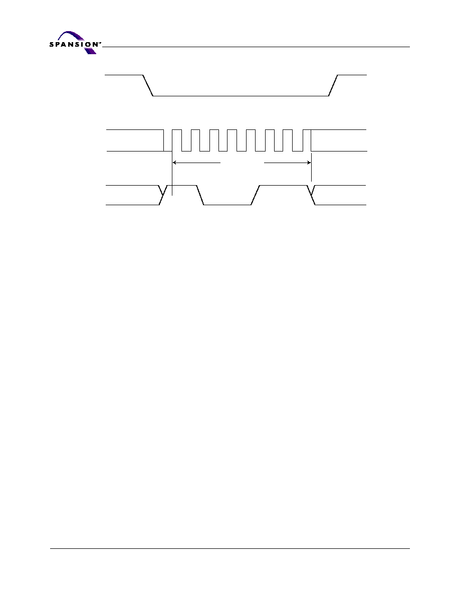
Bulk Erase (BE)
The Bulk Erase (BE) instruction sets to 1 (FFh) all bits inside the entire memory.
Before it can be accepted, a Write Enable (WREN) instruction must previously
have been executed. After the Write Enable (WREN) instruction has been de-
coded, the device sets the Write Enable Latch (WEL).
The Bulk Erase (BE) instruction is entered by driving Chip Select (CS#) Low, fol-
lowed by the instruction code, on Serial Data Input (SI). No address is required
for the Bulk Erase (BE) instruction. Chip Select (CS#) must be driven Low for the
entire duration of the sequence.
The instruction sequence is shown in
Figure 13
.
Chip Select (CS#) must be driven High after the eighth bit of the last address byte
has been latched in, otherwise the Bulk Erase (BE) instruction is not executed.
As soon as Chip Select (CS#) is driven High, the self-timed Bulk Erase cycle
(whose duration is t
BE
) is initiated. While the Bulk Erase cycle is in progress, the
Status Register may be read to check the value of the Write In Progress (WIP)
bit. The Write In Progress (WIP) bit is 1 during the self-timed Bulk Erase cycle,
and is 0 when it is completed. At some unspecified time before the cycle is com-
pleted, the Write Enable Latch (WEL) bit is reset.
A Bulk Erase (BE) instruction is executed only if all the Block Protect (BP2, BP1,
BP0) bits (see Table
1
) are set to 0. The Bulk Erase (BE) instruction is ignored if
one or more sectors are protected.
CS#
SCK
SI
Instruction
24 Bit Address
0
1
2
3
4
5
6
7
8
9
10
28 29 30 31
23 22 21
3
2
1
0
MSB
22
S25FL Family (Serial Peripheral Interface) S25FL004D
S25FL004D_00A0 June 28, 2004
A d v a n c e I n f o r m a t i o n
Figure 13. Bulk Erase (BE) Instruction Sequence
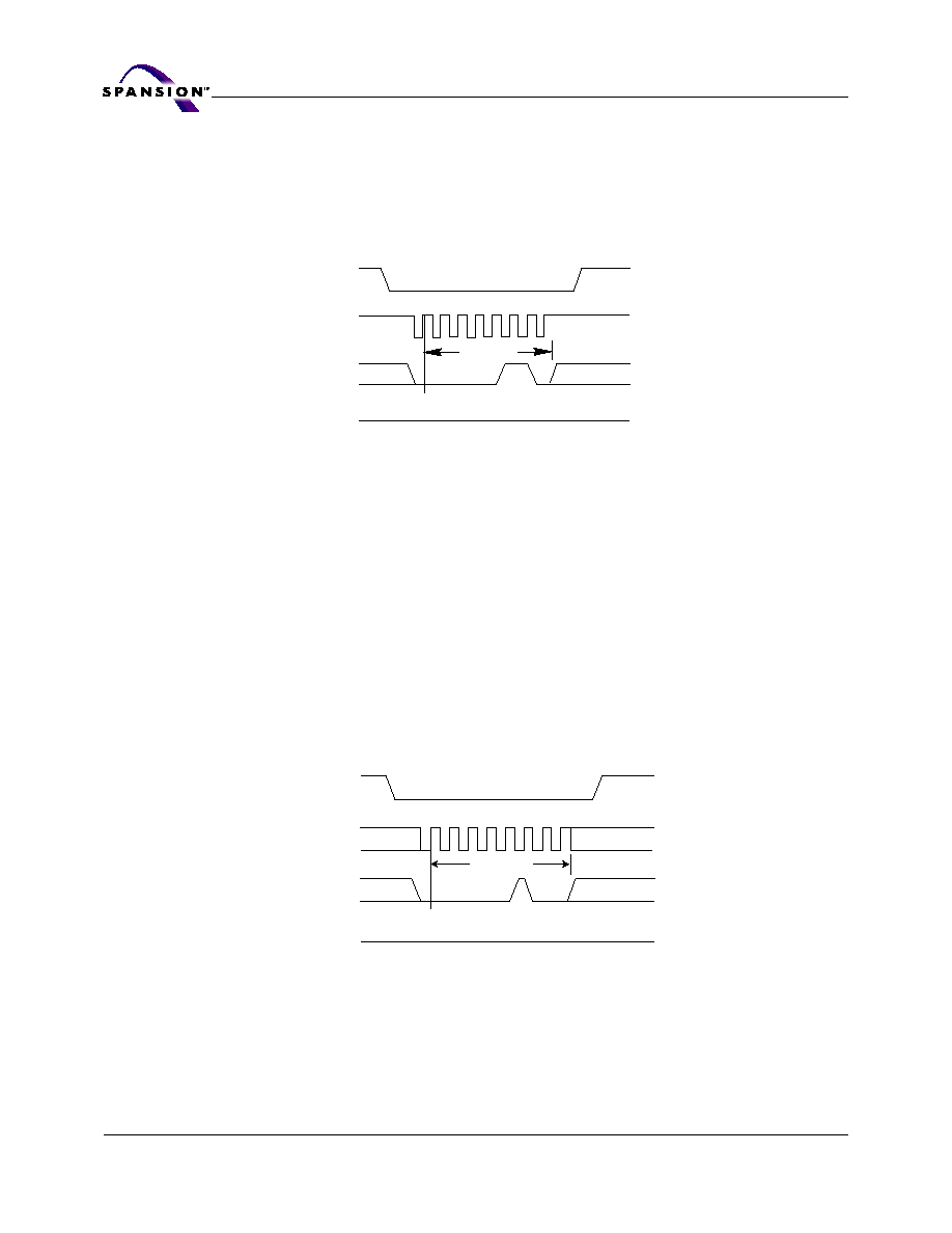
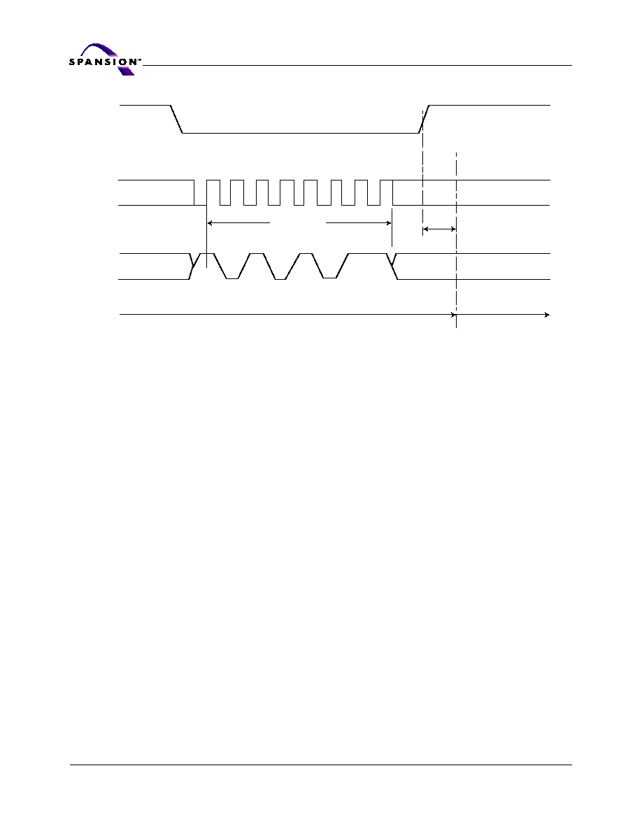
Deep Power Down (DP)
The Deep Power Down (DP) instruction puts the device in the lowest current
mode of 1 µA typical.
It is recommended that the standard Standby mode be used for the lowest power
current draw, as well as the Deep Power Down (DP) as an extra software protec-
tion mechanism when this device is not in active use. In this mode, the device
ignores all Write, Program and Erase instructions. Chip Select (CS#) must be
driven Low for the entire duration of the sequence.
The Deep Power Down (DP) instruction is entered by driving Chip Select (CS#)
Low, followed by the instruction code on Serial Data Input (SI). Chip Select (CS#)
must be driven Low for the entire duration of the sequence.
The instruction sequence is shown in
Figure 14
.
Driving Chip Select (CS#) High after the eighth bit of the instruction code has
been latched puts the device in Deep Power Down mode. The Deep Power Down
mode can only be entered by executing the Deep Power Down (DP) instruction to
reduce the standby current (from I
SB
to I
DP
as specified in Table
6
). As soon as
Chip Select (CS#) is driven high, it requires a delay of t
DP
currently in progress
before Deep Power Down mode is entered.
Once the device has entered the Deep Power Down mode, all instructions are ig-
nored except the Release from Deep Power Down (RES) and Read Electronic
Signature. This releases the device from the Deep Power Down mode. The Re-
lease from Deep Power Down and Read Electronic Signature (RES) instruction
also allows the Electronic Signature of the device to be output on Serial Data Out-
put (SO).
The Deep Power Down mode automatically stops at Power-down, and the device
always powers up in the Standby mode.
Any Deep Power Down (DP) instruction, while an Erase, Program or WRSR cycle
is in progress, is rejected without having any effect on the cycle in progress.
0
1
2
4
5
6
7
Instruction
CS#
SCK
SI
3

June 28, 2004 S25FL004D_00A0
S25FL Family (Serial Peripheral Interface) S25FL004D
23
A d v a n c e I n f o r m a t i o n
Figure 14. Deep Power Down (DP) Instruction Sequence
Release from Deep Power Down (RES)
The Release from Deep Power Down (RES) instruction provides the only way to
exit the Deep Power Down mode. Once the device has entered the Deep Power
Down mode, all instructions are ignored except the Release from Deep Power
Down (RES) instruction. Executing this instruction takes the device out of Deep
Power Down mode.
The Release from Deep Power Down (RES) instruction is entered by driving Chip
Select (CS#) Low, followed by the instruction code on Serial Data Input (SI). Chip
Select (CS#) must be driven Low for the entire duration of the sequence.
The instruction sequence is shown in
Figure 15
.
Driving Chip Select (CS#) High after the 8-bit instruction byte has been received
by the device, but before the whole of the 8-bit Electronic Signature has been
transmitted for the first time, still insures that the device is put into Standby
mode. If the device was previously in the Deep Power Down mode, though, the
transition to the Stand-by Power mode is delayed by t
RES
, and Chip Select (CS#)
must remain High for at least t
RES(max)
, as specified in Table
8
. Once in the Stand-
by Power mode, the device waits to be selected, so that it can receive, decode
and execute instructions.
CS#
SCK
SI
Standby Mode
Deep Power Down Mode
Instruction
0
1
2
3
4
5
6
7
t
DP
24
S25FL Family (Serial Peripheral Interface) S25FL004D
S25FL004D_00A0 June 28, 2004
A d v a n c e I n f o r m a t i o n
Figure 15. Release from Deep Power Down Instruction Sequence
Release from Deep Power Down and Read Electronic Signature (RES)
Once the device has entered Deep Power Down mode, all instructions are ignored
except the RES instruction. The RES instruction can also be used to read the 8-
bit Electronic Signature of the device on the SO pin. The RES instruction always
provides access to the Electronic Signature of the device (except while an Erase,
Program or WRSR cycle is in progress), and can be applied even if DP mode has
not been entered. Any RES instruction executed while an Erase, Program or
WRSR cycle is in progress is not decoded, and has no effect on the cycle in
progress.
The device features an 8-bit Electronic Signature, whose value for the S25FL004D
is 12h. This can be read using RES instruction.
The device is first selected by driving Chip Select (CS#) Low. The instruction code
is followed by 3 dummy bytes, each bit being latched-in on Serial Data Input (SI)
during the rising edge of Serial Clock (SCK). Then, the 8-bit Electronic Signature,
stored in the memory, is shifted out on Serial Data Output (SO), each bit being
shifted out during the falling edge of Serial Clock (SCK).
The instruction sequence is shown in
Figure 16
.
The Release from Deep Power Down and Read Electronic Signature (RES) is ter-
minated by driving Chip Select (CS#) High after the Electronic Signature has
been read at least once. Sending additional clock cycles on Serial Clock (SCK),
while Chip Select (CS#) is driven Low, causes the Electronic Signature to be out-
put repeatedly.
When Chip Select is driven High, the device is put in the Stand-by Power mode.
If the device was not previously in the Deep Power Down mode, the transition to
the Stand-by Power mode is immediate. If the device was previously in the Deep
Power Down mode, though, the transition to the Standby mode is delayed by
t
RES
, and Chip Select (CS#) must remain High for at lease t
RES(max)
, as specified
in Table
8
. Once in the Stand-by Power mode, the device waits to be selected, so
that it can receive, decode and execute instructions.
CS#
SCK
SI
0
1
2
3
4
5
6
7
Instruction
Deep Power Down Mode
t
RES
Standby Mode

June 28, 2004 S25FL004D_00A0
S25FL Family (Serial Peripheral Interface) S25FL004D
25
A d v a n c e I n f o r m a t i o n
Figure 16. Release from Deep Power Down and Read Electronic Signature (RES) Instruction Sequence
CS#
SCK
SI
SO
3 Dummy
Bytes
High Impedance
MSB
Deep Power Down Mode
Standby Mode
0
1
2
3
4
5
6
7
8
9
10
28 29 30 31 32 33 34 35 36 37 38
Electronic ID
Instruction
t
RES
23 22 21
3
2
1
0
7
6
5
4
3
2
1
0

26
S25FL Family (Serial Peripheral Interface) S25FL004D
S25FL004D_00A0 June 28, 2004
A d v a n c e I n f o r m a t i o n
Power-up and Power-down
The device must not be selected at power-up or power-down (that is, CS# must
follow the voltage applied on V
CC
) until V
CC
reaches the correct value as follows:
V
CC
(min) at power-up, and then for a further delay of t
PU
(as described in
Table
5
)
V
SS
at power-down
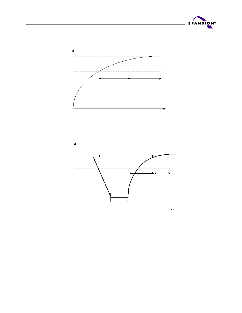
A simple pull-up resistor on Chip Select (CS#) can usually be used to insure safe
and proper power-up and power-down.
The device ignores all instructions until a time delay of t
PU
(as described in Table
5
) has elapsed after the moment that V
CC
rises above the minimum V
CC
thresh-
old. However, correct operation of the device is not guaranteed if by this time V
CC
is still below V
CC
(min). No Write Status Register, Program or Erase instructions
should be sent until t
PU
after V
CC
reaches the minimum V
CC
threshold (See
Figure
17
).
At power-up, the device is in Standby mode (not Deep Power Down mode) and
the WEL bit is reset.
During Power-down or voltage drops, the power down must drop below the V
CC
(low) for a period of minimum t
PD
for the device to initialize correctly on power
up. (See Figure 18).
Normal precautions must be taken for supply rail decoupling to stabilize the V
CC
feed. Each device in a system should have the V
CC
rail decoupled by a suitable
capacitor close to the package pins (this capacitor is generally of the order of 0.1
µF).
At power-down, when V
CC
drops from the operating voltage to below the mini-
mum V
CC
threshold, all operations are disabled and the device does not respond
to any instructions. (The designer needs to be aware that if a power-down occurs
while a Write, Program or Erase cycle is in progress, data corruption can result.)
June 28, 2004 S25FL004D_00A0
S25FL Family (Serial Peripheral Interface) S25FL004D
27
A d v a n c e I n f o r m a t i o n
Figure 17. Power-Up Timing
Figure 18. Power-Down and Voltage Drop
Vcc
(max)
Vcc
(min)
Vcc
time
t
PU
Full Device Access
VCC
VCC (max)
VCC (min)
VCC (low)
Device Access Allowed
No Device Access Allowed
Time
tPU
tPD
28
S25FL Family (Serial Peripheral Interface) S25FL004D
S25FL004D_00A0 June 28, 2004
A d v a n c e I n f o r m a t i o n
Table 5. Power-Up Timing
Initial Delivery State
The device is delivered with all bits set to 1 (each byte contains FFh). The Status
Register contains 00h (all Status Register bits are 0).
Maximum Rating
Stressing the device above the rating listed in the Absolute Maximum Ratings
section below may cause permanent damage to the device. These are stress rat-
ings only and operation of the device at these or any other conditions above those
indicated in the Operating sections of this specification is not implied. Exposure
to Absolute Maximum Rating conditions for extended periods may affect device
reliability
Absolute Maximum Ratings
Ambient Storage Temperature . . . . . . . . . . . . . . . . . . . . . ≠65∞C to +150∞C
Voltage with Respect to Ground:
All Inputs and I/Os. . . . . . . . . . . . . . . . . . . . . . . . . . . . . . . . ≠0.3 V to 4.5 V
Operating Ranges
Ambient Operating Temperature (T
A
)
Commercial . . . . . . . . . . . . . . . . . . . . . . . . . . . . . . . . . . . . . 0∞C to +70∞C
Industrial . . . . . . . . . . . . . . . . . . . . . . . . . . . . . . . . . . . . . ≠40∞C to +85∞C
Positive Power Supply
Voltage Range . . . . . . . . . . . . . . . . . . . . . . . . . . . . . . . . . . . .2.7 V to 3.6 V
Operating ranges define those limits between which functionality of the device is guaranteed.
Symbol
Parameter
Min
Max
Unit
V
CC(min)
V
CC
(minimum)
2.7
V
V
CC(low)
V
CC
(low)
V
t
PU
V
CC
(min) to device operation
2
ms
t
PD
V
CC
(low) duration
ns

June 28, 2004 S25FL004D_00A0
S25FL Family (Serial Peripheral Interface) S25FL004D
29
A d v a n c e I n f o r m a t i o n
DC Characteristics
This section summarizes the DC and AC Characteristics of the device. Designers
should check that the operating conditions in their circuit match the measure-
ment conditions specified in the Test Specifications in Table
7
, when relying on
the quoted parameters.
CMOS Compatible
Table 6. DC Characteristics
Notes:Typical values are at T
A
= 25
∞
C and 3.0 V.
Parameter Description
Test Conditions
Min
Typ.
Max
Unit
V
CC
Supply Voltage
2.7
3
3.6
V
I
CC1
Active Read Current
SCK = 0.1 V
CC
/0.9V
CC
33 MHz
mA
SCK = 0.1 V
CC
/0.9V
CC
V
CC
= 3.0V
50 MHz
9
12
I
CC2
Active Page Program Current
CS# = V
CC
23
mA
I
CC3
Active WRSR Current
CS# = V
CC
23
mA
I
CC4
Active Sector Erase Current
CS# = V
CC
23
mA
I
CC5
Active Bulk Erase Current
CS# = V
CC
23
mA
I
SB
Standby Current
V
CC
= 3.0 V
CS# = V
CC
50
µA
I
DP
Deep Power Down Current
V
CC
= 3.0 V
CS# = V
CC
1
5
µA
I
LI
Input Leakage Current
V
IN
= GND to V
CC
1
µA
I
LO
Output Leakage Current
V
IN
= GND to V
CC
1
µA
V
IL
Input Low Voltage
≠0.3
0.3 V
CC
V
V
IH
Input High Voltage
0.7 V
CC
V
CC
+ 0.5
V
V
OL
Output Low Voltage
I
OL
= 1.6 mA, V
CC
= V
CC
min
0.4
V
V
OH
Output High Voltage
I
OH
= ≠0.1 mA
V
CC
≠ 0.2
V

30
S25FL Family (Serial Peripheral Interface) S25FL004D
S25FL004D_00A0 June 28, 2004
A d v a n c e I n f o r m a t i o n
Test Conditions
Figure 19. AC Measurements I/O Waveform
Table 7. Test Specifications
Symbol
Parameter
Min
Max
Unit
C
L
Load Capacitance
30
pF
Input Rise and Fall Times
5
ns
Input Pulse Voltage
0.2 V
CC
to 0.8 V
CC
V
Input and Output Timing
Reference Voltages
0.3 V
CC
to 0.7 V
CC
V
0.8 V
CC
0.2 V
CC
0.7 V
CC
0.3 V
CC
Input Levels
Input and Output
Timing Reference levels
0.5 V
CC

June 28, 2004 S25FL004D_00A0
S25FL Family (Serial Peripheral Interface) S25FL004D
31
A d v a n c e I n f o r m a t i o n
AC Characteristics
Table 8. AC Characteristics
Note:
1. Typical program and erase times assume the following conditions: 25C, VCC = 3.0V; 10, 000 cycles; checkerboard
data pattern
2. Under worst-case conditions of 90C; VCC = 2.7V; 100,000 cycles
3. Not 100% tested
Symbol
Parameter
Min
Typ
Max
Unit
F
SCK
SCK Clock Frequency READ instruction
D.C.
33
MHz
F
SCK
SCK Clock Frequency for:
FAST_READ, PP, SE, BE, DP, RES, WREN,
WRDI, RDSR, WRSR
D.C.
50
MHz
t
CRT
Clock Rise Time (Slew Rate)
0.1
V/ns
t
CFT
Clock Fall Time (Slew Rate)
0.1
V/ns
t
WH
SCK High Time
9
ns
t
WL
SCK Low Time
9
ns
t
CS
CS# High Time
100
ns
t
CSS
(Note 3)
CS# Setup Time
5
ns
t
CSH
(Note 3)
CS# HOLD Time
5
ns
t
HD
(Note 3)
HOLD# Setup Time (relative to SCK)
5
ns
t
CD
(Note 3)
HOLD# Hold Time (relative to SCK)
5
ns
t
HC
HOLD# Setup Time (relative to SCK)
5
ns
t
CH
HOLD# Hold Time (relative to SCK)
5
ns
t
V
Output Valid
9
ns
t
HO
Output Hold Time
0
ns
t
HD:DAT
Data in Hold Time
5
ns
t
SU:DAT
Data in Setup Time
5
ns
t
R
Input Rise Time
5
ns
t
F
Input Fall Time
5
ns
t
LZ
(Note 3)
HOLD# to Output Low Z
9
ns
t
HZ
(Note 3)
HOLD# to Output High Z
9
ns
t
DIS
(Note 3)
Output Disable Time
9
ns
t
WPS
(Note 3)
Write Protect Setup Time
20
ns
t
WPH
(Note 3)
Write Protect Hold Time
100
ns
t
RES
Release DP Mode
3
µs
t
DP
CS# High to Deep Power Down Mode
3
µs
t
W
Write Status Register Time
20 (Note 2)
ns
t
PP
Page Programming Time
1.5 (Note 1)
2 (Note 2)
ms
t
SE
Sector Erase Time
0.5 (Note 1)
0.8 (Note 2)
sec
t
BE
Bulk Erase Time
4 (Note 1)
7 (Note 2)
sec

32
S25FL Family (Serial Peripheral Interface) S25FL004D
S25FL004D_00A0 June 28, 2004
A d v a n c e I n f o r m a t i o n
AC Characteristics
Figure 20. SPI Mode 0 (0,0) Input Timing
Figure 21. SPI Mode 0 (0,0) Output Timing
CS#
SCK
SI
SO
t
CSH
t
CSS
t
CSH
t
CSS
t
CRT
t
CFT
MSB IN
LSB IN
High Impedance
t
SU:DAT
t
HD:DAT
t
CS
CS#
SCK
SO
LSB OUT
t
WH
t
WL
t
DIS
t
V
t
HO
t
V
t
HO

June 28, 2004 S25FL004D_00A0
S25FL Family (Serial Peripheral Interface) S25FL004D
33
A d v a n c e I n f o r m a t i o n
AC Characteristics
Figure 22. HOLD# Timing
Figure 23. Write Protect Setup and Hold Timing during WRSR when SRWD=1
t
CH
t
HZ
t
CD
t
HD
t
HC
t
LZ
CS#
SCK
SO
SI
HOLD#
W#
CS#
SCK
SI
SO
High Impedance
t
WPS
t
WPH

34
S25FL Family (Serial Peripheral Interface) S25FL004D
S25FL004D_00A0 June 28, 2004
A d v a n c e I n f o r m a t i o n
Physical Dimensions
S08 wide--8-pin Plastic Small Outline 208mils Body Width Package

June 28, 2004 S25FL004D_00A0
S25FL Family (Serial Peripheral Interface) S25FL004D
35
A d v a n c e I n f o r m a t i o n
Physical Dimensions
8-Contact WSON (6mm x 5mm) Leadless Package

36
S25FL Family (Serial Peripheral Interface) S25FL004D
S25FL004D_00A0 June 28, 2004
A d v a n c e I n f o r m a t i o n
Revision Summary
Revision A (June 28, 2004)
Initial release.
Trademarks and Notice
The contents of this document are subject to change without notice. This document may contain information on a Spansion product under development by
FASL LLC. FASL LLC reserves the right to change or discontinue work on any product without notice. The information in this document is provided as is
without warranty or guarantee of any kind as to its accuracy, completeness, operability, fitness for particular purpose, merchantability, non-infringement of
third-party rights, or any other warranty, express, implied, or statutory. FASL LLC assumes no liability for any damages of any kind arising out of the use of
the information in this document.
Copyright © 2004 FASL LLC. All rights reserved.
Spansion, the Spansion logo, MirrorBit, combinations thereof, and ExpressFlash are trademarks of FASL LLC. Other company and product names used in this
publication are for identification purposes only and may be trademarks of their respective companies.