
"This document states the current technical specifications regarding the Spansion product(s) described herein. Spansion LLC deems the products
to have been in sufficient production volume such that subsequent versions of this document are not expected to change. However, typographical
or specification corrections, or modifications to the valid combinations offered may occur."
Publication Number S29AL008D_00 Revision A Amendment 3 Issue Date June 16, 2005
This document has not been approved. Sharing this document with non-Spansion employees violates QS9000/TS16949 requirements.
S29AL008D
8 Megabit (1 M x 8-Bit/512 K x 16-Bit)
CMOS 3.0 Volt-only Boot Sector Flash Memory
Data Sheet
Distinctive Characteristics
Architectural Advantage
Single power supply operation
-- 2.7 to 3.6 volt read and write operations for battery-
powered applications
Manufactured on 200nm process technology
-- Compatible with 0.32 µm and 230nm Am29LV160
devices
Flexible sector architecture
-- One 16 Kbyte, two 8 Kbyte, one 32 Kbyte, and fifteen
64 Kbyte sectors (byte mode)
-- One 8 Kword, two 4 Kword, one 16 Kword, and fifteen
32 Kword sectors (word mode)
-- Supports full chip erase
-- Sector Protection features:
-- A hardware method of locking a sector to prevent
any program or erase operations within that sector
-- Sectors can be locked in-system or via programming
equipment
-- Temporary Sector Unprotect feature allows code
changes in previously locked sectors
Unlock Bypass Program Command
-- Reduces overall programming time when issuing
multiple program command sequences
Top or bottom boot block configurations
available
Embedded Algorithms
-- Embedded Erase algorithm automatically
preprograms and erases the entire chip or any
combination of designated sectors
-- Embedded Program algorithm automatically writes
and verifies data at specified addresses
Compatibility with JEDEC standards
-- Pinout and software compatible with single-power
supply Flash
-- Superior inadvertent write protection
Performance Characteristics
High performance
-- Access times as fast as 55 ns
-- Extended temperature range (-40∞C to +125∞C)
Ultra low power consumption (typical values
at 5 MHz)
-- 200 nA Automatic Sleep mode current
-- 200 nA standby mode current
-- 7 mA read current
-- 15 mA program/erase current
Cycling endurance: 1,000,000 cycles per
sector typical
Data retention: 20 years typical
-- Reliable operation for the life of the system
Package option
48-ball FBGA
48-pin TSOP
44-pin SO
Software Features
Data# Polling and toggle bits
-- Provides a software method of detecting program or
erase operation completion
Erase Suspend/Erase Resume
-- Suspends an erase operation to read data from, or
program data to, a sector that is not being erased,
then resumes the erase operation
Hardware Features
Ready/Busy# pin (RY/BY#)
-- Provides a hardware method of detecting program or
erase cycle completion
Hardware reset pin (RESET#)
-- Hardware method to reset the device to reading array
data

2
S29AL008D
S29AL008D_00A3 June 16, 2005
D a t a S h e e t
Notice On Data Sheet Designations
Spansion LLC issues data sheets with Advance Information or Preliminary designations to advise
readers of product information or intended specifications throughout the product life cycle, in-
cluding development, qualification, initial production, and full production. In all cases, however,
readers are encouraged to verify that they have the latest information before finalizing their de-
sign. The following descriptions of Spansion data sheet designations are presented here to high-
light their presence and definitions.
Advance Information
The Advance Information designation indicates that Spansion LLC is developing one or more spe-
cific products, but has not committed any design to production. Information presented in a doc-
ument with this designation is likely to change, and in some cases, development on the product
may discontinue. Spansion LLC therefore places the following conditions upon Advance Informa-
tion content:
"This document contains information on one or more products under development at Spansion LLC. The
information is intended to help you evaluate this product. Do not design in this product without con-
tacting the factory. Spansion LLC reserves the right to change or discontinue work on this proposed
product without notice."
Preliminary
The Preliminary designation indicates that the product development has progressed such that a
commitment to production has taken place. This designation covers several aspects of the prod-
uct life cycle, including product qualification, initial production, and the subsequent phases in the
manufacturing process that occur before full production is achieved. Changes to the technical
specifications presented in a Preliminary document should be expected while keeping these as-
pects of production under consideration. Spansion places the following conditions upon Prelimi-
nary content:
"This document states the current technical specifications regarding the Spansion product(s) described
herein. The Preliminary status of this document indicates that product qualification has been completed,
and that initial production has begun. Due to the phases of the manufacturing process that require
maintaining efficiency and quality, this document may be revised by subsequent versions or modifica-
tions due to changes in technical specifications."
Combination
Some data sheets will contain a combination of products with different designations (Advance In-
formation, Preliminary, or Full Production). This type of document will distinguish these products
and their designations wherever necessary, typically on the first page, the ordering information
page, and pages with DC Characteristics table and AC Erase and Program table (in the table
notes). The disclaimer on the first page refers the reader to the notice on this page.
Full Production (No Designation on Document)
When a product has been in production for a period of time such that no changes or only nominal
changes are expected, the Preliminary designation is removed from the data sheet. Nominal
changes may include those affecting the number of ordering part numbers available, such as the
addition or deletion of a speed option, temperature range, package type, or V
IO
range. Changes
may also include those needed to clarify a description or to correct a typographical error or incor-
rect specification. Spansion LLC applies the following conditions to documents in this category:
"This document states the current technical specifications regarding the Spansion product(s) described
herein. Spansion LLC deems the products to have been in sufficient production volume such that sub-
sequent versions of this document are not expected to change. However, typographical or specification
corrections, or modifications to the valid combinations offered may occur."
Questions regarding these document designations may be directed to your local AMD or Fujitsu
sales office.

June 16, 2005 S29AL008D_00A3
S29AL008D
3
D a t a S h e e t
General Description
The S29AL008D is an 8 Mbit, 3.0 volt-only Flash memory organized as 1,048,576
bytes or 524,288 words. The device is offered in 48-ball FBGA, 44-pin SO, and
48-pin TSOP packages. For more information, refer to publication number 21536.
The word-wide data (x16) appears on DQ15≠DQ0; the byte-wide (x8) data ap-
pears on DQ7≠DQ0. This device requires only a single, 3.0 volt V
CC
supply to
perform read, program, and erase operations. A standard EPROM programmer
can also be used to program and erase the device.
This device is manufactured using Spansion's 200nm process technology, and of-
fers all the features and benefits of the Am29LV800B, which was manufactured
using 0.32 µm process technology.
The standard device offers access times of 70, 90, and 120 ns, allowing high
speed microprocessors to operate without wait states. To eliminate bus conten-
tion the device contains separate chip enable (CE#), write enable (WE#) and
output enable (OE#) controls.
The device requires only a single 3.0 volt power supply for both read and write
functions. Internally generated and regulated voltages are provided for the pro-
gram and erase operations.
The device is entirely command set compatible with the JEDEC single-power-
supply Flash standard. Commands are written to the command register using
standard microprocessor write timings. Register contents serve as input to an in-
ternal state-machine that controls the erase and programming circuitry. Write
cycles also internally latch addresses and data needed for the programming and
erase operations. Reading data out of the device is similar to reading from other
Flash or EPROM devices.
Device programming occurs by executing the program command sequence. This
initiates the Embedded Program algorithm--an internal algorithm that auto-
matically times the program pulse widths and verifies proper cell margin. The
Unlock Bypass mode facilitates faster programming times by requiring only two
write cycles to program data instead of four.
Device erasure occurs by executing the erase command sequence. This initiates
the Embedded Erase algorithm--an internal algorithm that automatically
preprograms the array (if it is not already programmed) before executing the
erase operation. During erase, the device automatically times the erase pulse
widths and verifies proper cell margin.
The host system can detect whether a program or erase operation is complete by
observing the RY/BY# pin, or by reading the DQ7 (Data# Polling) and DQ6 (tog-
gle) status bits. After a program or erase cycle is completed, the device is ready
to read array data or accept another command.
The sector erase architecture allows memory sectors to be erased and repro-
grammed without affecting the data contents of other sectors. The device is fully
erased when shipped from the factory.
Hardware data protection measures include a low V
CC
detector that automat-
ically inhibits write operations during power transitions. The hardware sector
protection feature disables both program and erase operations in any combina-
tion of the sectors of memory. This can be achieved in-system or via
programming equipment.

4
S29AL008D
S29AL008D_00A3 June 16, 2005
D a t a S h e e t
The Erase Suspend feature enables the user to put erase on hold for any period
of time to read data from, or program data to, any sector that is not selected for
erasure. True background erase can thus be achieved.
The hardware RESET# pin terminates any operation in progress and resets the
internal state machine to reading array data. The RESET# pin may be tied to the
system reset circuitry. A system reset would thus also reset the device, enabling
the system microprocessor to read the boot-up firmware from the Flash memory.
The device offers two power-saving features. When addresses are stable for a
specified amount of time, the device enters the automatic sleep mode. The
system can also place the device into the standby mode. Power consumption is
greatly reduced in both these modes.
Spansion's Flash technology combines years of Flash memory manufacturing ex-
perience to produce the highest levels of quality, reliability and cost
effectiveness. The device electrically erases all bits within a sector simulta-
neously via Fowler-Nordheim tunneling. The data is programmed using hot
electron injection.

June 16, 2005 S29AL008D_00A3
S29AL008D
5
D a t a S h e e t
Table Of Contents
Product Selector Guide. . . . . . . . . . . . . . . . . . . . . . 6
Block Diagram . . . . . . . . . . . . . . . . . . . . . . . . . . . . . 6
Connection Diagrams . . . . . . . . . . . . . . . . . . . . . . . 7
Special Handling Instructions for FBGA Package . . . . . . . . . . . . . . . . . 8
Pin Configuration. . . . . . . . . . . . . . . . . . . . . . . . . . . 9
Logic Symbol . . . . . . . . . . . . . . . . . . . . . . . . . . . . . . 9
Ordering Information . . . . . . . . . . . . . . . . . . . . . . 10
Standard Products . . . . . . . . . . . . . . . . . . . . . . . . . . . . . . . . . . . . . . . . .10
Device Bus Operations . . . . . . . . . . . . . . . . . . . . . . 11
Table 1. S29AL008D Device Bus Operations . . . . . . . . . . . . . . . . . . . . . .11
Word/Byte Configuration . . . . . . . . . . . . . . . . . . . . . . . . . . . . . . . . . . . 11
Requirements for Reading Array Data . . . . . . . . . . . . . . . . . . . . . . . . . 11
Writing Commands/Command Sequences . . . . . . . . . . . . . . . . . . . . . 12
Program and Erase Operation Status . . . . . . . . . . . . . . . . . . . . . . . . . .12
Standby Mode . . . . . . . . . . . . . . . . . . . . . . . . . . . . . . . . . . . . . . . . . . . . .12
Automatic Sleep Mode . . . . . . . . . . . . . . . . . . . . . . . . . . . . . . . . . . . . . 13
RESET#: Hardware Reset Pin . . . . . . . . . . . . . . . . . . . . . . . . . . . . . . . . 13
Output Disable Mode . . . . . . . . . . . . . . . . . . . . . . . . . . . . . . . . . . . . . . 13
Table 2. S29AL008D Top Boot Block Sector Addresses . . . . . . . . . . . 14
Table 3. S29AL008D Bottom Boot Block Sector Addresses . . . . . . . . 15
Autoselect Mode . . . . . . . . . . . . . . . . . . . . . . . . . . . . . . . . . . . . . . . . . . 15
Table 4. S29AL008D Autoselect Codes (High Voltage Method) . . . . . 16
Sector Protection/Unprotection . . . . . . . . . . . . . . . . . . . . . . . . . . . . . . 16
Temporary Sector Unprotect . . . . . . . . . . . . . . . . . . . . . . . . . . . . . . . . 16
Figure 1. Temporary Sector Unprotect Operation . . . . . . . . . . . . . . . . . 17
Figure 2. In-System Sector Protect/Sector Unprotect Algorithms. . . . . 18
Hardware Data Protection . . . . . . . . . . . . . . . . . . . . . . . . . . . . . . . . . .19
Command Definitions . . . . . . . . . . . . . . . . . . . . . . 19
Reading Array Data . . . . . . . . . . . . . . . . . . . . . . . . . . . . . . . . . . . . . . . .19
Reset Command . . . . . . . . . . . . . . . . . . . . . . . . . . . . . . . . . . . . . . . . . 20
Autoselect Command Sequence . . . . . . . . . . . . . . . . . . . . . . . . . . . . . 20
Word/Byte Program Command Sequence . . . . . . . . . . . . . . . . . . . . . 20
Figure 3. Program Operation . . . . . . . . . . . . . . . . . . . . . . . . . . . . . . . . . 22
Chip Erase Command Sequence . . . . . . . . . . . . . . . . . . . . . . . . . . . . . 22
Sector Erase Command Sequence . . . . . . . . . . . . . . . . . . . . . . . . . . . 23
Erase Suspend/Erase Resume Commands . . . . . . . . . . . . . . . . . . . . . 23
Figure 4. Erase Operation. . . . . . . . . . . . . . . . . . . . . . . . . . . . . . . . . . . . 25
Table 5. S29AL008D Command Definitions . . . . . . . . . . . . . . . . . . . . . . 25
Write Operation Status . . . . . . . . . . . . . . . . . . . . 27
DQ7: Data# Polling . . . . . . . . . . . . . . . . . . . . . . . . . . . . . . . . . . . . . . . 27
Figure 5. Data# Polling Algorithm . . . . . . . . . . . . . . . . . . . . . . . . . . . . . 28
RY/BY#: Ready/Busy# . . . . . . . . . . . . . . . . . . . . . . . . . . . . . . . . . . . . . 28
DQ6: Toggle Bit I . . . . . . . . . . . . . . . . . . . . . . . . . . . . . . . . . . . . . . . . . 29
DQ2: Toggle Bit II . . . . . . . . . . . . . . . . . . . . . . . . . . . . . . . . . . . . . . . . 29
Reading Toggle Bits DQ6/DQ2 . . . . . . . . . . . . . . . . . . . . . . . . . . . . . . 30
DQ5: Exceeded Timing Limits . . . . . . . . . . . . . . . . . . . . . . . . . . . . . . . 30
DQ3: Sector Erase Timer . . . . . . . . . . . . . . . . . . . . . . . . . . . . . . . . . . 30
Figure 6. Toggle Bit Algorithm . . . . . . . . . . . . . . . . . . . . . . . . . . . . . . . . . 31
Table 6. Write Operation Status . . . . . . . . . . . . . . . . . . . . . . . . . . . . . . 32
Absolute Maximum Ratings . . . . . . . . . . . . . . . . . 33
Operating Ranges . . . . . . . . . . . . . . . . . . . . . . . . . . 33
Figure 7. Maximum Negative Overshoot Waveform . . . . . . . . . . . . . . . 33
Figure 8. Maximum Positive Overshoot Waveform . . . . . . . . . . . . . . . . 33
DC Characteristics . . . . . . . . . . . . . . . . . . . . . . . . . 34
Figure 9. I
CC1
Current vs. Time (Showing Active and
Automatic Sleep Currents). . . . . . . . . . . . . . . . . . . . . . . . . . . . . . . . . . . . 35
Figure 10. Typical I
CC1
vs. Frequency . . . . . . . . . . . . . . . . . . . . . . . . . . . . 35
Test Conditions . . . . . . . . . . . . . . . . . . . . . . . . . . . 36
Figure 11. Test Setup . . . . . . . . . . . . . . . . . . . . . . . . . . . . . . . . . . . . . . . . 36
Table 7. Test Specifications . . . . . . . . . . . . . . . . . . . . . . . . . . . . . . . . . . . 36
Key to Switching Waveforms . . . . . . . . . . . . . . . . 37
Figure 12. Input Waveforms and Measurement Levels . . . . . . . . . . . . . . 37
AC Characteristics . . . . . . . . . . . . . . . . . . . . . . . . . 38
Table 8. Read Operations . . . . . . . . . . . . . . . . . . . . . . . . . . . . . . . . . . . . 38
Figure 13. Read Operations Timings. . . . . . . . . . . . . . . . . . . . . . . . . . . . 38
Table 9. Hardware Reset (RESET#) . . . . . . . . . . . . . . . . . . . . . . . . . . . . 39
Figure 14. RESET# Timings . . . . . . . . . . . . . . . . . . . . . . . . . . . . . . . . . . . 39
Table 10. Word/Byte Configuration (BYTE#) . . . . . . . . . . . . . . . . . . . .40
Figure 15. BYTE# Timings for Read Operations . . . . . . . . . . . . . . . . . . . 41
Figure 16. BYTE# Timings for Write Operations . . . . . . . . . . . . . . . . . . 41
Erase / Program Operations . . . . . . . . . . . . . . . . . . . . . . . . . . . . . . . . 42
Figure 17. Program Operation Timings . . . . . . . . . . . . . . . . . . . . . . . . . 43
Figure 18. Chip/Sector Erase Operation Timings . . . . . . . . . . . . . . . . . 44
Figure 19. Data# Polling Timings (During Embedded Algorithms) . . . . 45
Figure 20. Toggle Bit Timings (During Embedded Algorithms) . . . . . . 45
Figure 21. DQ2 vs. DQ6 . . . . . . . . . . . . . . . . . . . . . . . . . . . . . . . . . . . . . 46
Table 11. Temporary Sector Unprotect . . . . . . . . . . . . . . . . . . . . . . . . . . 46
Figure 22. Temporary Sector Unprotect Timing Diagram . . . . . . . . . . 46
Figure 23. Sector Protect/Unprotect Timing Diagram . . . . . . . . . . . . . 47
Table 12. Alternate CE# Controlled Erase/Program Operations . . . . . 48
Figure 24. Alternate CE# Controlled Write Operation Timings. . . . . 49
Erase and Programming Performance. . . . . . . . . 49
Table 13. Latchup Characteristics . . . . . . . . . . . . . . . . . . . . . . . . . . . . . . 50
Table 14. TSOP, SO, and BGA Pin Capacitance . . . . . . . . . . . . . . . . . . . 50
Physical Dimensions . . . . . . . . . . . . . . . . . . . . . . . . 51
TS 048--48-Pin Standard TSOP . . . . . . . . . . . . . . . . . . . . . . . . . . . . . 51
VBK 048 - 48 Ball Fine-Pitch Ball Grid Array (FBGA)
8.15 x 6.15 mm . . . . . . . . . . . . . . . . . . . . . . . . . . . . . . . . . . . . . . . . . . . . .52
SO 044--44-Pin Small Outline Package . . . . . . . . . . . . . . . . . . . . . . .53
Revision Summary . . . . . . . . . . . . . . . . . . . . . . . . . 54
6
S29AL008D
S29AL008D_00A3 June 16, 2005
D a t a S h e e t
Product Selector Guide
Note: See
AC Characteristics, on page 38
for full specifications.
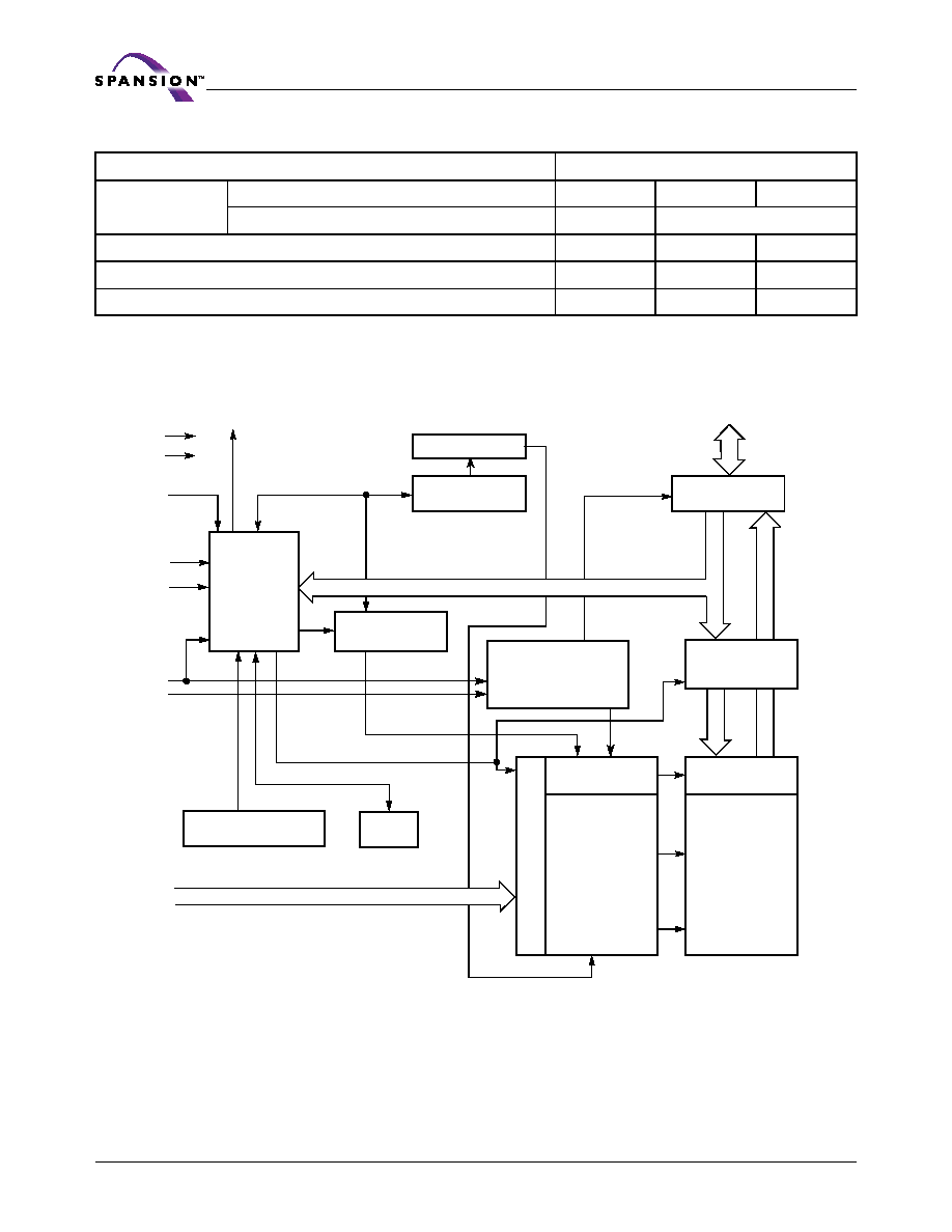
Block Diagram
Family Part Number
S29AL008D
Speed Options
Full Voltage Range: V
CC
= 2.7 ≠ 3.6 V
70
90
Regulated Voltage Range: V
CC
= 3.0 ≠ 3.6V
55
Max access time, ns (t
ACC
)
55
70
90
Max CE# access time, ns (t
CE
)
55
70
90
Max OE# access time, ns (t
OE
)
30
30
35
Input/Output
Buffers
X-Decoder
Y-Decoder
Chip Enable
Output Enable
Logic
Erase Voltage
Generator
PGM Voltage
Generator
Timer
V
CC
Detector
State
Control
Command
Register
V
CC
V
SS
WE#
BYTE#
CE#
OE#
STB
STB
DQ0≠DQ15 (A-1)
Sector Switches
RY/BY#
RESET#
Data
Latch
Y-Gating
Cell Matrix
A
ddr
e
ss La
t
c
h
A0≠A18
June 16, 2005 S29AL008D_00A3
S29AL008D
7
D a t a S h e e t
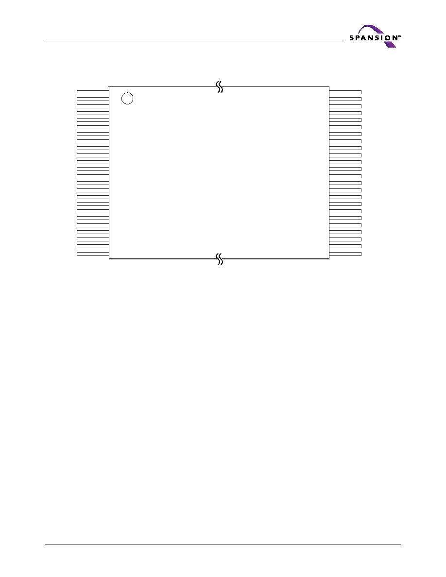
Connection Diagrams
A1
A15
A18
A14
A13
A12
A11
A10
A9
A8
NC
NC
WE#
RESET#
NC
NC
RY/BY#
A17
A7
A6
A5
A4
A3
A2
1
16
2
3
4
5
6
7
8
17
18
19
20
21
22
23
24
9
10
11
12
13
14
15
A16
DQ2
BYTE#
VSS
DQ15/A-1
DQ7
DQ14
DQ6
DQ13
DQ9
DQ1
DQ8
DQ0
OE#
VSS
CE#
A0
DQ5
DQ12
DQ4
VCC
DQ11
DQ3
DQ10
48
33
47
46
45
44
43
42
41
40
39
38
37
36
35
34
25
32
31
30
29
28
27
26
Standard TSOP
8
S29AL008D
S29AL008D_00A3 June 16, 2005
D a t a S h e e t
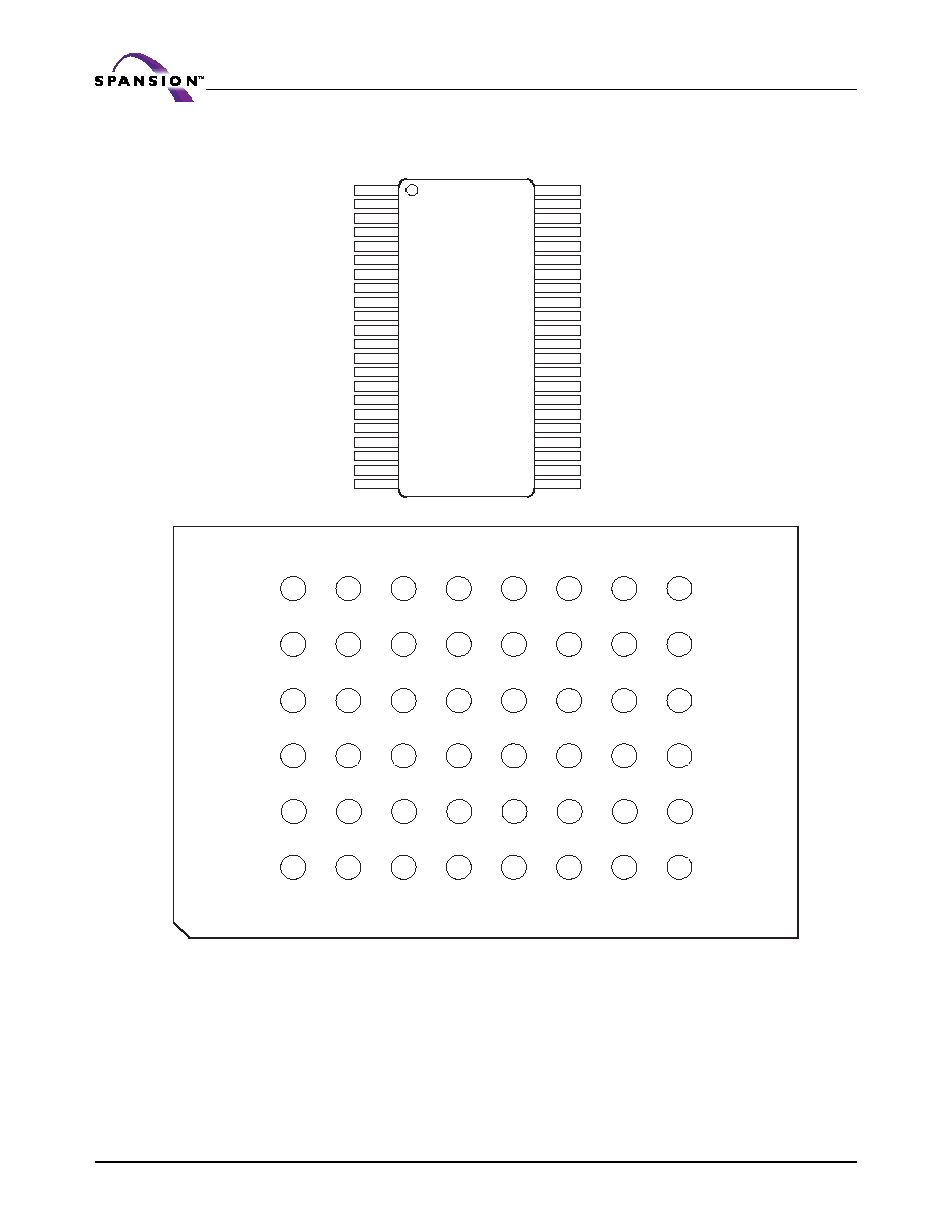
Connection Diagrams
Special Handling Instructions for FBGA Package
Special handling is required for Flash Memory products in FBGA packages.Flash
memory devices in FBGA packages may be damaged if exposed to ultrasonic
cleaning methods. The package and/or data integrity may be compromised if the
package body is exposed to temperatures above 150∞C for prolonged periods of
time.
A1
B1
C1
D1
E1
F1
G1
H1
A2
B2
C2
D2
E2
F2
G2
H2
A3
B3
C3
D3
E3
F3
G3
H3
A4
B4
C4
D4
E4
F4
G4
H4
A5
B5
C5
D5
E5
F5
G5
H5
A6
B6
C6
D6
E6
F6
G6
H6
DQ15/A-1
VSS
BYTE#
A16
A15
A14
A12
A13
DQ13
DQ6
DQ14
DQ7
A11
A10
A8
A9
VCC
DQ4
DQ12
DQ5
NC
NC
RESET#
WE#
DQ11
DQ3
DQ10
DQ2
NC
A18
NC
RY/BY#
DQ9
DQ1
DQ8
DQ0
A5
A6
A17
A7
OE#
VSS
CE#
A0
A1
A2
A4
A3
1
2
3
4
5
6
7
8
9
10
11
12
13
14
15
16
17
18
19
20
21
22
RY/BY#
A18
A17
A7
A6
A5
A4
A3
A2
A1
A0
CE#
VSS
OE#
DQ0
DQ8
DQ1
DQ9
DQ2
DQ10
DQ3
DQ11
44
43
42
41
40
39
38
37
36
35
34
33
32
31
30
29
28
27
26
25
24
23
RESET#
WE#
A8
A9
A10
A11
A12
A13
A14
A15
A16
BYTE#
VSS
DQ15/A-1
DQ7
DQ14
DQ6
DQ13
DQ5
DQ12
DQ4
VCC
SO
FBGA
Top View, Balls Facing Down
June 16, 2005 S29AL008D_00A3
S29AL008D
9
D a t a S h e e t
Pin Configuration
A0≠A18
=
19 addresses
DQ0≠DQ14
=
15 data inputs/outputs
DQ15/A-1
=
DQ15 (data input/output, word
mode),
A-1 (LSB address input, byte
mode)
BYTE#
=
Selects 8-bit or 16-bit mode
CE#
=
Chip enable
OE#
= Output
enable
WE#
=
Write enable
RESET#
=
Hardware reset pin, active low
RY/BY#
= Ready/Busy#
output
V
CC
=
3.0 volt-only single power supply
(see Product Selector Guide for speed
options and voltage supply tolerances)
V
SS
=
Device ground
NC
=
Pin not connected internally
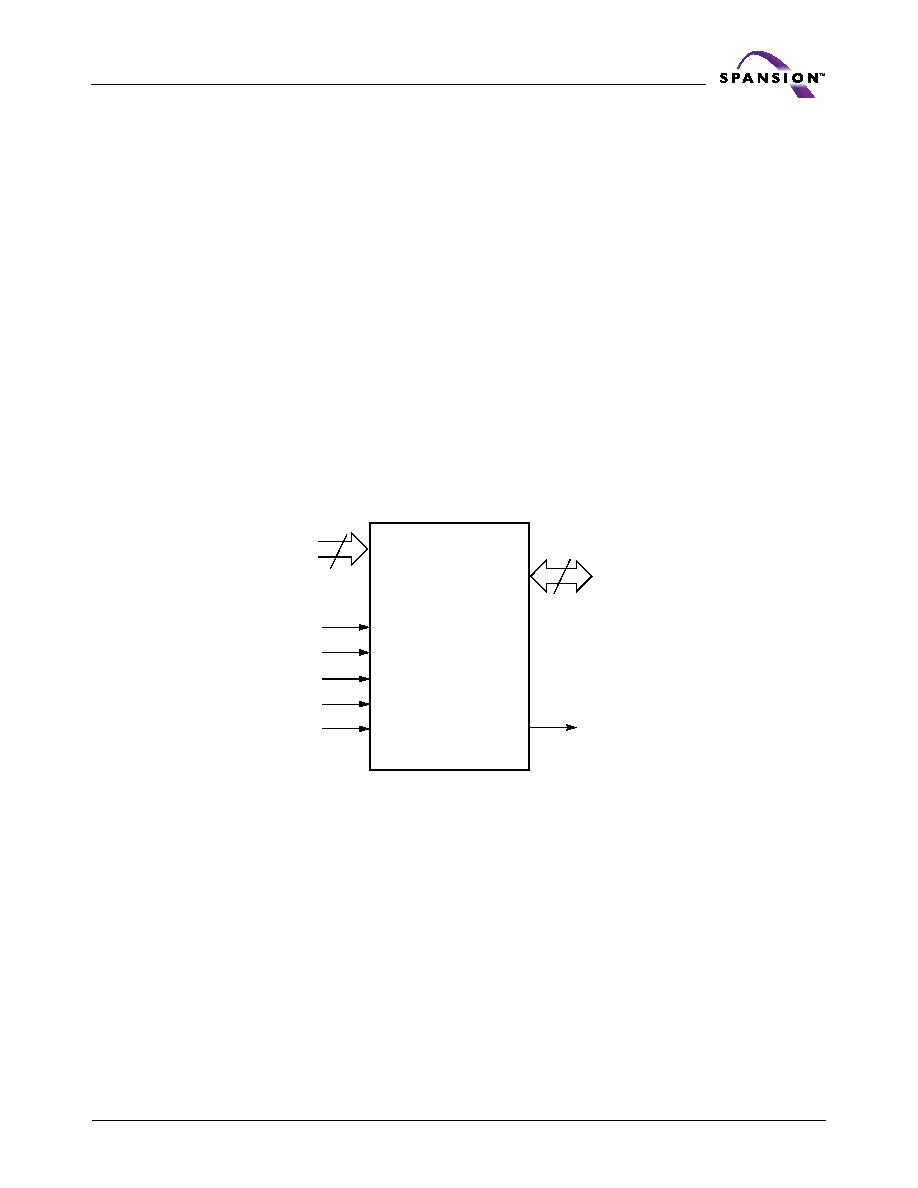
Logic Symbol
19
16 or 8
DQ0≠DQ15
(A-1)
A0≠A18
CE#
OE#
WE#
RESET#
BYTE#
RY/BY#

10
S29AL008D
S29AL008D_00A3 June 16, 2005
D a t a S h e e t
Ordering Information
Standard Products
Spansion standard products are available in several packages and operating
ranges. The order number (Valid Combination) is formed by a combination of the
elements below.
Notes:
1. Type 0 is standard. Specify other options as required.
2. Type 1 is standard. Specify other options as required.
3. TSOP and SOP package markings omit packing type designator from ordering part number.
4. BGA package marking omits leading S29 and packing type designator from ordering part number.
Valid Combinations
Valid Combinations list configurations planned to be supported in volume for this device. Consult
your local sales office to confirm availability of specific valid combinations and to check on newly
released combinations.
S29AL008D
55
T
A
I
RI
0
PACKING TYPE
0
= Tray
1
= Tube
2
= 7" Tape and Reel
3
= 13" Tape and Reel
MODEL NUMBER
01
= x8/x16, V
CC
= 2.7 - 3.6V, top boot sector device
R1
= x8/x16, V
CC
= 3.0 - 3.6V. top boot sector device
02
= x8/x16, V
CC
= 2.7 - 3.6V, bottom boot sector device
R2
= x8/x16, V
CC
= 3.0 - 3.6V. bottom boot sector device
TEMPERATURE RANGE
I =
Industrial
(-40
∞
C to +85
∞
C)
N
= Extended (-40∞C to +125∞C)
PACKAGE MATERIAL SET
A
= Standard
F
= Pb-Free
PACKAGE TYPE
T
= Thin Small Outline Package (TSOP) Standard Pinout
B
= Fine-pitch Ball-Grid Array Package
M
= Small Outline Package (SOP) Standard Pinout
SPEED OPTION
55
= 55 ns Access Speed
70
= 70 ns Access Speed
90
= 90 ns Access Speed
DEVICE NUMBER/DESCRIPTION
S29AL008D
8 Megabit Flash Memory manufactured using 200 nm process technology
3.0 Volt-only Read, Program, and Erase
S29AL008D Valid Combinations
Package Description
Device Number
Speed
Option
Package Type,
Material, and
Temperature Range
Model
Number
Packing Type
S29AL008D
55
TAI, TFI
R1, R2
0, 3 (
Note 1
)
TS048 (
Note 3
)
TSOP
70, 90
TAI, TFI, TAN, TFN
01, 02
55
BAI, BFI
R1, R2
0, 2, 3 (
Note 1
)
VBK048 (
Note 4
)
Fine-Pitch BGA
70, 90
BAI, BF, BAN, BFN
01, 02
55
MAI, MFI
R1, R2
0, 1, 3 (
Note 2
)
SO044 (
Note 3
)
SOP
70, 90
MAI, MFI, MAN, MFN
01, 02

June 16, 2005 S29AL008D_00A3
S29AL008D
11
D a t a S h e e t
Device Bus Operations
This section describes the requirements and use of the device bus operations,
which are initiated through the internal command register. The command register
itself does not occupy any addressable memory location. The register is com-
posed of latches that store the commands, along with the address and data
information needed to execute the command. The contents of the register serve
as inputs to the internal state machine. The state machine outputs dictate the
function of the device.
Table 1
lists the device bus operations, the inputs and con-
trol levels they require, and the resulting output. The following subsections
describe each of these operations in further detail.
Legend:
L = Logic Low = V
IL
, H = Logic High = V
IH
, V
ID
= 12.0 ± 0.5 V, X = Don't Care, A
IN
= Address In, D
IN
= Data In, D
OUT
= Data Out
Notes:
1. Addresses are A18:A0 in word mode (BYTE# = V
IH
), A18:A-1 in byte mode (BYTE# = V
IL
).
2. The sector protect and sector unprotect functions may also be implemented via programming equipment. See the
Sector Protection/Unprotection, on page 16
.
Word/Byte Configuration
The BYTE# pin controls whether the device data I/O pins DQ15≠DQ0 operate in
the byte or word configuration. If the BYTE# pin is set at logic 1, the device is in
word configuration, DQ15≠DQ0 are active and controlled by CE# and OE#.
If the BYTE# pin is set at logic 0, the device is in byte configuration, and only data
I/O pins DQ0≠DQ7 are active and controlled by CE# and OE#. The data I/O pins
DQ8≠DQ14 are tri-stated, and the DQ15 pin is used as an input for the LSB (A-1)
address function.
Requirements for Reading Array Data
To read array data from the outputs, the system must drive the CE# and OE#
pins to V
IL
. CE# is the power control and selects the device. OE# is the output
control and gates array data to the output pins. WE# should remain at V
IH
. The
BYTE# pin determines whether the device outputs array data in words or bytes.
Table 1. S29AL008D Device Bus Operations
Operation
CE# OE# WE# RESET#
Addresses
(
Note 1
)
DQ0≠
DQ7
DQ8≠DQ15
BYTE#
= V
IH
BYTE#
= V
IL
Read
L
L
H
H
A
IN
D
OUT
D
OUT
DQ8≠DQ14 = High-Z,
DQ15 = A-1
Write
L
H
L
H
A
IN
D
IN
D
IN
Standby
V
CC
±
0.3 V
X
X
V
CC
±
0.3 V
X
High-Z High-Z
High-Z
Output Disable
L
H
H
H
X
High-Z High-Z
High-Z
Reset
X
X
X
L
X
High-Z High-Z
High-Z
Sector Protect (
Note 2
)
L
H
L
V
ID
Sector Address,
A6 = L, A1 = H,
A0 = L
D
IN
X
X
Sector Unprotect (
Note 2
)
L
H
L
V
ID
Sector Address,
A6 = H, A1 = H,
A0 = L
D
IN
X
X
Temporary Sector Unprotect
X
X
X
V
ID
A
IN
D
IN
D
IN
High-Z

12
S29AL008D
S29AL008D_00A3 June 16, 2005
D a t a S h e e t
The internal state machine is set for reading array data upon device power-up,
or after a hardware reset. This ensures that no spurious alteration of the memory
content occurs during the power transition. No command is necessary in this
mode to obtain array data. Standard microprocessor read cycles that assert valid
addresses on the device address inputs produce valid data on the device data
outputs. The device remains enabled for read access until the command register
contents are altered.
See
Reading Array Data, on page 19
for more information. Refer to the AC table
for timing specifications and to
Figure 13, on page 38
for the timing diagram. I
CC1
in the DC Characteristics table represents the active current specification for
reading array data.
Writing Commands/Command Sequences
To write a command or command sequence (which includes programming data
to the device and erasing sectors of memory), the system must drive WE# and
CE# to V
IL
, and OE# to V
IH
.
For program operations, the BYTE# pin determines whether the device accepts
program data in bytes or words. Refer to
Word/Byte Configuration, on page 11
for more information.
The device features an Unlock Bypass mode to facilitate faster programming.
Once the device enters the Unlock Bypass mode, only two write cycles are re-
quired to program a word or byte, instead of four. The
Word/Byte Program
Command Sequence, on page 20
contains details on programming data to the
device using both standard and Unlock Bypass command sequences.
An erase operation can erase one sector, multiple sectors, or the entire device.
Table 2, on page 14
and
Table 3, on page 15
indicate the address space that each
sector occupies. A sector address consists of the address bits required to uniquely
select a sector. The
Command Definitions, on page 19
contains details on erasing
a sector or the entire chip, or suspending/resuming the erase operation.
After the system writes the autoselect command sequence, the device enters the
autoselect mode. The system can then read autoselect codes from the internal
register (which is separate from the memory array) on DQ7≠DQ0. Standard read
cycle timings apply in this mode. Refer to the
Autoselect Mode, on page 15
and
Autoselect Command Sequence, on page 20
for more information.
I
CC2
in the DC Characteristics table represents the active current specification for
the write mode. The
AC Characteristics, on page 38
contains timing specification
tables and timing diagrams for write operations.
Program and Erase Operation Status
During an erase or program operation, the system may check the status of the
operation by reading the status bits on DQ7≠DQ0. Standard read cycle timings
and I
CC
read specifications apply. Refer to
Write Operation Status, on page 27
for more information, and to
AC Characteristics, on page 38
for timing diagrams.
Standby Mode
When the system is not reading or writing to the device, it can place the device
in the standby mode. In this mode, current consumption is greatly reduced, and
the outputs are placed in the high impedance state, independent of the OE#
input.

June 16, 2005 S29AL008D_00A3
S29AL008D
13
D a t a S h e e t
The device enters the CMOS standby mode when the CE# and RESET# pins are
both held at V
CC
± 0.3 V. (Note that this is a more restricted voltage range than
V
IH
.) If CE# and RESET# are held at V
IH
, but not within V
CC
± 0.3 V, the device
is in the standby mode, but the standby current is greater. The device requires
standard access time (t
CE
) for read access when the device is in either of these
standby modes, before it is ready to read data.
If the device is deselected during erasure or programming, the device draws ac-
tive current until the operation is completed.
In the DC Characteristics table, I
CC3
and I
CC4
represents the standby current
specification.
Automatic Sleep Mode
The automatic sleep mode minimizes Flash device energy consumption. The de-
vice automatically enables this mode when addresses remain stable for t
ACC
+ 30
ns. The automatic sleep mode is independent of the CE#, WE#, and OE# control
signals. Standard address access timings provide new data when addresses are
changed. While in sleep mode, output data is latched and always available to the
system. I
CC4
in the DC Characteristics table represents the automatic sleep mode
current specification.
RESET#: Hardware Reset Pin
The RESET# pin provides a hardware method of resetting the device to reading
array data. When the RESET# pin is driven low for at least a period of t
RP
, the
device immediately terminates any operation in progress, tristates all output
pins, and ignores all read/write commands for the duration of the RESET# pulse.
The device also resets the internal state machine to reading array data. The op-
eration that was interrupted should be reinitiated once the device is ready to
accept another command sequence, to ensure data integrity.
Current is reduced for the duration of the RESET# pulse. When RESET# is held
at V
SS
±0.3 V, the device draws CMOS standby current (I
CC4
). If RESET# is held
at V
IL
but not within V
SS
±0.3 V, the standby current is greater.
The RESET# pin may be tied to the system reset circuitry. A system reset would
thus also reset the Flash memory, enabling the system to read the boot-up firm-
ware from the Flash memory.
If RESET# is asserted during a program or erase operation, the RY/BY# pin re-
mains a 0 (busy) until the internal reset operation is complete, which requires a
time of t
READY
(during Embedded Algorithms). The system can thus monitor RY/
BY# to determine whether the reset operation is complete. If RESET# is asserted
when a program or erase operation is not executing (RY/BY# pin is 1), the reset
operation is completed within a time of t
READY
(not during Embedded Algorithms).
The system can read data t
RH
after the RESET# pin returns to V
IH
.
Refer to
AC Characteristics, on page 38
for RESET# parameters and to
Figure
14, on page 39
for the timing diagram.
Output Disable Mode
When the OE# input is at V
IH
, output from the device is disabled. The output pins
are placed in the high impedance state.

14
S29AL008D
S29AL008D_00A3 June 16, 2005
D a t a S h e e t
Table 2. S29AL008D Top Boot Block Sector Addresses
Sector
A18
A17
A16
A15
A14
A13
A12
Sector Size
(Kbytes/
Kwords)
Address Range (in hexadecimal)
(x8)
Address Range
(x16)
Address Range
SA0
0
0
0
0
X
X
X
64/32
00000h≠0FFFFh
00000h≠07FFFh
SA1
0
0
0
1
X
X
X
64/32
10000h≠1FFFFh
08000h≠0FFFFh
SA2
0
0
1
0
X
X
X
64/32
20000h≠2FFFFh
10000h≠17FFFh
SA3
0
0
1
1
X
X
X
64/32
30000h≠3FFFFh
18000h≠1FFFFh
SA4
0
1
0
0
X
X
X
64/32
40000h≠4FFFFh
20000h≠27FFFh
SA5
0
1
0
1
X
X
X
64/32
50000h≠5FFFFh
28000h≠2FFFFh
SA6
0
1
1
0
X
X
X
64/32
60000h≠6FFFFh
30000h≠37FFFh
SA7
0
1
1
1
X
X
X
64/32
70000h≠7FFFFh
38000h≠3FFFFh
SA8
1
0
0
0
X
X
X
64/32
80000h≠8FFFFh
40000h≠47FFFh
SA9
1
0
0
1
X
X
X
64/32
90000h≠9FFFFh
48000h≠4FFFFh
SA10
1
0
1
0
X
X
X
64/32
A0000h≠AFFFFh
50000h≠57FFFh
SA11
1
0
1
1
X
X
X
64/32
B0000h≠BFFFFh
58000h≠5FFFFh
SA12
1
1
0
0
X
X
X
64/32
C0000h≠CFFFFh
60000h≠67FFFh
SA13
1
1
0
1
X
X
X
64/32
D0000h≠DFFFFh
68000h≠6FFFFh
SA14
1
1
1
0
X
X
X
64/32
E0000h≠EFFFFh
70000h≠77FFFh
SA15
1
1
1
1
0
X
X
32/16
F0000h≠F7FFFh
78000h≠7BFFFh
SA16
1
1
1
1
1
0
0
8/4
F8000h≠F9FFFh
7C000h≠7CFFFh
SA17
1
1
1
1
1
0
1
8/4
FA000h≠FBFFFh
7D000h≠7DFFFh
SA18
1
1
1
1
1
1
X
16/8
FC000h≠FFFFFh
7E000h≠7FFFFh

June 16, 2005 S29AL008D_00A3
S29AL008D
15
D a t a S h e e t
Note for Tables and : Address range is A18:A-1 in byte mode and A18:A0 in word mode. See
Word/Byte Configura-
tion, on page 11
.
Autoselect Mode
The autoselect mode provides manufacturer and device identification, and sector
protection verification, through identifier codes output on DQ7≠DQ0. This mode
is primarily intended for programming equipment to automatically match a device
to be programmed with its corresponding programming algorithm. However, the
autoselect codes can also be accessed in-system through the command register.
When using programming equipment, the autoselect mode requires V
ID
(11.5 V
to 12.5 V) on address pin A9. Address pins A6, A1, and A0 must be as shown in
Table 4, on page 16
. In addition, when verifying sector protection, the sector ad-
dress must appear on the appropriate highest order address bits (see
Table 2, on
page 14
and
Table 3, on page 15
).
Table 4, on page 16
shows the remaining ad-
dress bits that are don't care. When all necessary bits are set as required, the
programming equipment may then read the corresponding identifier code on
DQ7≠DQ0.
To access the autoselect codes in-system, the host system can issue the autose-
lect command via the command register, as shown in
Table 5, on page 25
. This
method does not require V
ID
. See
Command Definitions, on page 19
for details
on using the autoselect mode.
Table 3. S29AL008D Bottom Boot Block Sector Addresses
Sector
A18
A17
A16
A15
A14
A13
A12
Sector Size
(Kbytes/
Kwords)
Address Range (in hexadecimal)
(x8)
Address Range
(x16)
Address Range
SA0
0
0
0
0
0
0
X
16/8
00000h≠03FFFh
00000h≠01FFFh
SA1
0
0
0
0
0
1
0
8/4
04000h≠05FFFh
02000h≠02FFFh
SA2
0
0
0
0
0
1
1
8/4
06000h≠07FFFh
03000h≠03FFFh
SA3
0
0
0
0
1
X
X
32/16
08000h≠0FFFFh
04000h≠07FFFh
SA4
0
0
0
1
X
X
X
64/32
10000h≠1FFFFh
08000h≠0FFFFh
SA5
0
0
1
0
X
X
X
64/32
20000h≠2FFFFh
10000h≠17FFFh
SA6
0
0
1
1
X
X
X
64/32
30000h≠3FFFFh
18000h≠1FFFFh
SA7
0
1
0
0
X
X
X
64/32
40000h≠4FFFFh
20000h≠27FFFh
SA8
0
1
0
1
X
X
X
64/32
50000h≠5FFFFh
28000h≠2FFFFh
SA9
0
1
1
0
X
X
X
64/32
60000h≠6FFFFh
30000h≠37FFFh
SA10
0
1
1
1
X
X
X
64/32
70000h≠7FFFFh
38000h≠3FFFFh
SA11
1
0
0
0
X
X
X
64/32
80000h≠8FFFFh
40000h≠47FFFh
SA12
1
0
0
1
X
X
X
64/32
90000h≠9FFFFh
48000h≠4FFFFh
SA13
1
0
1
0
X
X
X
64/32
A0000h≠AFFFFh
50000h≠57FFFh
SA14
1
0
1
1
X
X
X
64/32
B0000h≠BFFFFh
58000h≠5FFFFh
SA15
1
1
0
0
X
X
X
64/32
C0000h≠CFFFFh
60000h≠67FFFh
SA16
1
1
0
1
X
X
X
64/32
D0000h≠DFFFFh
68000h≠6FFFFh
SA17
1
1
1
0
X
X
X
64/32
E0000h≠EFFFFh
70000h≠77FFFh
SA18
1
1
1
1
X
X
X
64/32
F0000h≠FFFFFh
78000h≠7FFFFh

16
S29AL008D
S29AL008D_00A3 June 16, 2005
D a t a S h e e t
L = Logic Low = V
IL
, H = Logic High = V
IH
, SA = Sector Address, X = Don't care.
Sector Protection/Unprotection
The hardware sector protection feature disables both program and erase opera-
tions in any sector. The hardware sector unprotection feature re-enables both
program and erase operations in previously protected sectors.
The device is shipped with all sectors unprotected. Spansion offers the option of
programming and protecting sectors at its factory prior to shipping the device
through Spansion's ExpressFlashTM Service. Contact an Spansion representative
for details.
It is possible to determine whether a sector is protected or unprotected. See
Autoselect Mode, on page 15
for details.
Sector Protection/unprotection can be implemented via two methods.
The primary method requires V
ID
on the RESET# pin only, and can be imple-
mented either in-system or via programming equipment.
Figure 2, on page 18
shows the algorithms and
Figure 23, on page 47
shows the timing diagram. This
method uses standard microprocessor bus cycle timing. For sector unprotect, all
unprotected sectors must first be protected prior to the first sector unprotect
write cycle.
The alternate method intended only for programming equipment requires V
ID
on
address pin A9 and OE#. This method is compatible with programmer routines
written for earlier 3.0 volt-only Spansion flash devices. Publication number 20536
contains further details; contact an Spansion representative to request a copy.
Temporary Sector Unprotect
This feature allows temporary unprotection of previously protected sectors to
change data in-system. The Sector Unprotect mode is activated by setting the
RESET# pin to V
ID
. During this mode, formerly protected sectors can be pro-
grammed or erased by selecting the sector addresses. Once V
ID
is removed from
the RESET# pin, all the previously protected sectors are protected again.
Table 4. S29AL008D Autoselect Codes (High Voltage Method)
Description
Mode
CE# OE# WE#
A18
to
A12
A11
to
A10 A9
A8
to
A7
A6
A5
to
A2
A1
A0
DQ8
to
DQ15
DQ7
to
DQ0
Manufacturer ID: Spansion
L
L
H
X
X
V
ID
X
L
X
L
L
X
01h
Device ID:
Am29LV800B
(Top Boot Block)
Word
L
L
H
X
X
V
ID
X
L
X
L
H
22h
DAh
Byte
L
L
H
X
DAh
Device ID:
Am29LV800B
(Bottom Boot
Block)
Word
L
L
H
X
X
V
ID
X
L
X
L
H
22h
5Bh
Byte
L
L
H
X
5Bh
Sector Protection
Verification
L
L
H
SA
X
V
ID
X
L
X
H
L
X
01h
(protected)
X
00h
(unprotected
)

June 16, 2005 S29AL008D_00A3
S29AL008D
17
D a t a S h e e t
Figure 1
shows the algorithm, and
Figure 22, on page 46
shows the timing dia-
grams, for this feature.
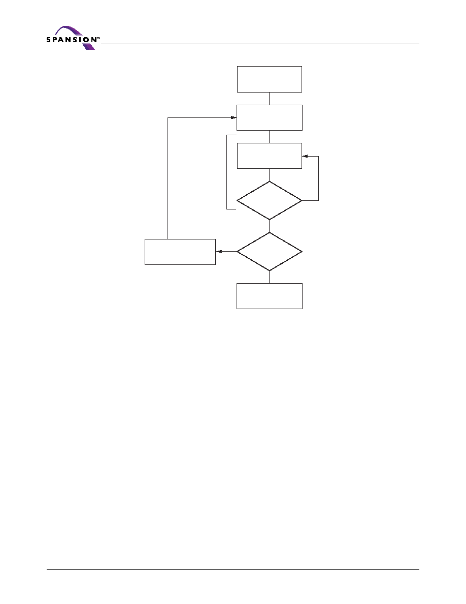
Figure 1. Temporary Sector Unprotect Operation
START
Perform Erase or
Program Operations
RESET# = V
IH
Temporary Sector
Unprotect Completed
(Note 2)
RESET# = V
ID
(Note 1)
Notes:
1. All protected sectors unprotected.
2. All previously protected sectors are protected once
again.
18
S29AL008D
S29AL008D_00A3 June 16, 2005
D a t a S h e e t
Figure 2. In-System Sector Protect/Sector Unprotect Algorithms
Sector Protect:
Write 60h to sector
address with
A6 = 0, A1 = 1,
A0 = 0
Set up sector
address
Wait 150 s
Verify Sector
Protect: Write 40h
to sector address
with A6 = 0,
A1 = 1, A0 = 0
Read from
sector address
with A6 = 0,
A1 = 1, A0 = 0
START
PLSCNT = 1
RESET# = V
ID
Wait 1 ms
First Write
Cycle = 60h?
Data = 01h?
Remove V
ID
from RESET#
Write reset
command
Sector Protect
complete
Yes
Yes
No
PLSCNT
= 25?
Yes
Device failed
Increment
PLSCNT
Temporary Sector
Unprotect Mode
No
Sector Unprotect:
Write 60h to sector
address with
A6 = 1, A1 = 1,
A0 = 0
Set up first sector
address
Wait 15 ms
Verify Sector
Unprotect: Write
40h to sector
address with
A6 = 1, A1 = 1,
A0 = 0
Read from
sector address
with A6 = 1,
A1 = 1, A0 = 0
START
PLSCNT = 1
RESET# = V
ID
Wait 1 ms
Data = 00h?
Last sector
verified?
Remove V
ID
from RESET#
Write reset
command
Sector Unprotect
complete
Yes
No
PLSCNT
= 1000?
Yes
Device failed
Increment
PLSCNT
Temporary Sector
Unprotect Mode
No
All sectors
protected?
Yes
Protect all sectors:
The indicated portion
of the sector protect
algorithm must be
performed for all
unprotected sectors
prior to issuing the
first sector
unprotect address
Set up
next sector
address
No
Yes
No
Yes
No
No
Yes
No
Sector Protect
Algorithm
Sector Unprotect
Algorithm
First Write
Cycle = 60h?
Protect another
sector?
Reset
PLSCNT = 1

June 16, 2005 S29AL008D_00A3
S29AL008D
19
D a t a S h e e t
Hardware Data Protection
The command sequence requirement of unlock cycles for programming or erasing
provides data protection against inadvertent writes (refer to
Table 5, on page 25
for command definitions). In addition, the following hardware data protection
measures prevent accidental erasure or programming, which might otherwise be
caused by spurious system level signals during V
CC
power-up and power-down
transitions, or from system noise.
Low V
CC
Write Inhibit
When V
CC
is less than V
LKO
, the device does not accept any write cycles. This pro-
tects data during V
CC
power-up and power-down. The command register and all
internal program/erase circuits are disabled, and the device resets. Subsequent
writes are ignored until V
CC
is greater than V
LKO
. The system must provide the
proper signals to the control pins to prevent unintentional writes when V
CC
is
greater than V
LKO
.
Write Pulse Glitch Protection
Noise pulses of less than 5 ns (typical) on OE#, CE# or WE# do not initiate a write
cycle.
Logical Inhibit
Write cycles are inhibited by holding any one of OE# = V
IL
, CE# = V
IH
or WE# =
V
IH
. To initiate a write cycle, CE# and WE# must be a logical zero while OE# is a
logical one.
Power-Up Write Inhibit
If WE# = CE# = V
IL
and OE# = V
IH
during power up, the device does not accept
commands on the rising edge of WE#. The internal state machine is automatically
reset to reading array data on power-up.
Command Definitions
Writing specific address and data commands or sequences into the command
register initiates device operations.
Table 5, on page 25
defines the valid register
command sequences. Writing incorrect address and data values or writing
them in the improper sequence resets the device to reading array data.
All addresses are latched on the falling edge of WE# or CE#, whichever happens
later. All data is latched on the rising edge of WE# or CE#, whichever happens
first. Refer to the appropriate timing diagrams in the
AC Characteristics, on
page 38
.
Reading Array Data
The device is automatically set to reading array data after device power-up. No
commands are required to retrieve data. The device is also ready to read array
data after completing an Embedded Program or Embedded Erase algorithm.
After the device accepts an Erase Suspend command, the device enters the Erase
Suspend mode. The system can read array data using the standard read timings,
except that if it reads at an address within erase-suspended sectors, the device
outputs status data. After completing a programming operation in the Erase Sus-
pend mode, the system may once again read array data with the same exception.
See
Erase Suspend/Erase Resume Commands, on page 23
for more information
on this mode.

20
S29AL008D
S29AL008D_00A3 June 16, 2005
D a t a S h e e t
The system must issue the reset command to re-enable the device for reading
array data if DQ5 goes high, or while in the autoselect mode. See the
Reset Com-
mand
, next.
See also
Requirements for Reading Array Data, on page 11
for more information.
The table provides the read parameters, and
Figure 13, on page 38
shows the
timing diagram.
Reset Command
Writing the reset command to the device resets the device to reading array data.
Address bits are don't care for this command.
The reset command may be written between the sequence cycles in an erase
command sequence before erasing begins. This resets the device to reading array
data. Once erasure begins, however, the device ignores reset commands until the
operation is complete.
The reset command may be written between the sequence cycles in a program
command sequence before programming begins. This resets the device to read-
ing array data (also applies to programming in Erase Suspend mode). Once
programming begins, however, the device ignores reset commands until the op-
eration is complete.
The reset command may be written between the sequence cycles in an autoselect
command sequence. Once in the autoselect mode, the reset command must be
written to return to reading array data (also applies to autoselect during Erase
Suspend).
If DQ5 goes high during a program or erase operation, writing the reset command
returns the device to reading array data (also applies during Erase Suspend).
Autoselect Command Sequence
The autoselect command sequence allows the host system to access the manu-
facturer and devices codes, and determine whether or not a sector is protected.
Table 5, on page 25
shows the address and data requirements. This method is an
alternative to that shown in
Table 4, on page 16
, which is intended for PROM pro-
grammers and requires V
ID
on address bit A9.
The autoselect command sequence is initiated by writing two unlock cycles, fol-
lowed by the autoselect command. The device then enters the autoselect mode,
and the system may read at any address any number of times, without initiating
another command sequence.
A read cycle at address XX00h retrieves the manufacturer code. A read cycle at
address XX01h in word mode (or 02h in byte mode) returns the device code. A
read cycle containing a sector address (SA) and the address 02h in word mode
(or 04h in byte mode) returns 01h if that sector is protected, or 00h if it is un-
protected. Refer to
Table 2, on page 14
and
Table 3, on page 15
for valid sector
addresses.
The system must write the reset command to exit the autoselect mode and return
to reading array data.
Word/Byte Program Command Sequence
The system may program the device by word or byte, depending on the state of
the BYTE# pin. Programming is a four-bus-cycle operation. The program com-
mand sequence is initiated by writing two unlock write cycles, followed by the

June 16, 2005 S29AL008D_00A3
S29AL008D
21
D a t a S h e e t
program set-up command. The program address and data are written next, which
in turn initiate the Embedded Program algorithm. The system is not required to
provide further controls or timings. The device automatically provides internally
generated program pulses and verifies the programmed cell margin.
Table 5, on
page 25
shows the address and data requirements for the byte program com-
mand sequence.
When the Embedded Program algorithm is complete, the device then returns to
reading array data and addresses are no longer latched. The system can deter-
mine the status of the program operation by using DQ7, DQ6, or RY/BY#. See
Write Operation Status, on page 27
for information on these status bits.
Any commands written to the device during the Embedded Program Algorithm
are ignored. Note that a hardware reset immediately terminates the program-
ming operation. The program command sequence should be reinitiated once the
device resets to reading array data, to ensure data integrity.
Programming is allowed in any sequence and across sector boundaries. A bit
cannot be programmed from a 0 back to a 1. Attempting to do so may halt
the operation and set DQ5 to 1, or cause the Data# Polling algorithm to indicate
the operation was successful. However, a succeeding read shows that the data is
still 0. Only erase operations can convert a 0 to a 1.
Unlock Bypass Command Sequence
The unlock bypass feature allows the system to program bytes or words to the
device faster than using the standard program command sequence. The unlock
bypass command sequence is initiated by first writing two unlock cycles. This is
followed by a third write cycle containing the unlock bypass command, 20h. The
device then enters the unlock bypass mode. A two-cycle unlock bypass program
command sequence is all that is required to program in this mode. The first cycle
in this sequence contains the unlock bypass program command, A0h; the second
cycle contains the program address and data. Additional data is programmed in
the same manner. This mode dispenses with the initial two unlock cycles required
in the standard program command sequence, resulting in faster total program-
ming time.
Table 5, on page 25
shows the requirements for the command
sequence.
During the unlock bypass mode, only the Unlock Bypass Program and Unlock By-
pass Reset commands are valid. To exit the unlock bypass mode, the system
must issue the two-cycle unlock bypass reset command sequence. The first cycle
must contain the data 90h; the second cycle the data 00h. Addresses are don't
care for both cycles. The device then returns to reading array data.
Figure 3, on page 22
illustrates the algorithm for the program operation. See
Erase / Program Operations, on page 42
i for parameters, and
Figure 17, on
page 43
for timing diagrams.
22
S29AL008D
S29AL008D_00A3 June 16, 2005
D a t a S h e e t
Note: See
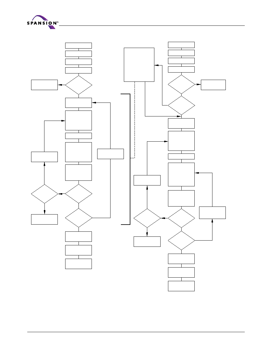
Table 5, on page 25
for program command sequence.
Figure 3. Program Operation
Chip Erase Command Sequence
Chip erase is a six bus cycle operation. The chip erase command sequence is ini-
tiated by writing two unlock cycles, followed by a set-up command. Two
additional unlock write cycles are then followed by the chip erase command,
which in turn invokes the Embedded Erase algorithm. The device does not require
the system to preprogram prior to erase. The Embedded Erase algorithm auto-
matically preprograms and verifies the entire memory for an all zero data pattern
prior to electrical erase. The system is not required to provide any controls or tim-
ings during these operations.
Table 5, on page 25
shows the address and data
requirements for the chip erase command sequence.
Any commands written to the chip during the Embedded Erase algorithm are ig-
nored. Note that a hardware reset during the chip erase operation immediately
terminates the operation. The Chip Erase command sequence should be reiniti-
ated once the device returns to reading array data, to ensure data integrity.
The system can determine the status of the erase operation by using DQ7, DQ6,
DQ2, or RY/BY#. See
Write Operation Status, on page 27
for information on
these status bits. When the Embedded Erase algorithm is complete, the device
returns to reading array data and addresses are no longer latched.
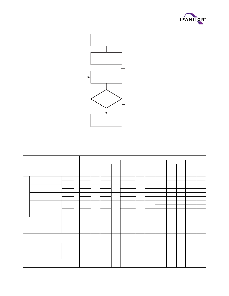
START
Write Program
Command Sequence
Data Poll
from System
Verify Data?
No
Yes
Last Address?
No
Yes
Programming
Completed
Increment Address
Embedded
Program
algorithm
in progress

June 16, 2005 S29AL008D_00A3
S29AL008D
23
D a t a S h e e t
Figure 4, on page 25
illustrates the algorithm for the erase operation. See
Erase
/ Program Operations, on page 42
for parameters, and
Figure 18, on page 44
for
timing diagrams.
Sector Erase Command Sequence
Sector erase is a six bus cycle operation. The sector erase command sequence is
initiated by writing two unlock cycles, followed by a set-up command. Two addi-
tional unlock write cycles are then followed by the address of the sector to be
erased, and the sector erase command.
Table 5, on page 25
shows the address
and data requirements for the sector erase command sequence.
The device does not require the system to preprogram the memory prior to erase.
The Embedded Erase algorithm automatically programs and verifies the sector for
an all zero data pattern prior to electrical erase. The system is not required to
provide any controls or timings during these operations.
After the command sequence is written, a sector erase time-out of 50 µs begins.
During the time-out period, additional sector addresses and sector erase com-
mands may be written. Loading the sector erase buffer may be done in any
sequence, and the number of sectors may be from one sector to all sectors. The
time between these additional cycles must be less than 50 µs, otherwise the last
address and command might not be accepted, and erasure may begin. It is rec-
ommended that processor interrupts be disabled during this time to ensure all
commands are accepted. The interrupts can be re-enabled after the last Sector
Erase command is written. If the time between additional sector erase commands
can be assumed to be less than 50 µs, the system need not monitor DQ3. Any
command other than Sector Erase or Erase Suspend during the time-out
period resets the device to reading array data. The system must rewrite the
command sequence and any additional sector addresses and commands.
The system can monitor DQ3 to determine if the sector erase timer has timed
out. (See
DQ3: Sector Erase Timer, on page 30
.) The time-out begins from the
rising edge of the final WE# pulse in the command sequence.
Once the sector erase operation begins, only the Erase Suspend command is
valid. All other commands are ignored. Note that a hardware reset during the
sector erase operation immediately terminates the operation. The Sector Erase
command sequence should be reinitiated once the device returns to reading array
data, to ensure data integrity.
When the Embedded Erase algorithm is complete, the device returns to reading
array data and addresses are no longer latched. The system can determine the
status of the erase operation by using DQ7, DQ6, DQ2, or RY/BY#. Refer to
Write
Operation Status, on page 27
for information on these status bits.
Figure 4, on page 25
illustrates the algorithm for the erase operation. Refer to
Erase / Program Operations, on page 42
for parameters, and to
Figure 18, on
page 44
for timing diagrams.
Erase Suspend/Erase Resume Commands
The Erase Suspend command allows the system to interrupt a sector erase oper-
ation and then read data from, or program data to, any sector not selected for
erasure. This command is valid only during the sector erase operation, including
the 50 µs time-out period during the sector erase command sequence. The Erase
Suspend command is ignored if written during the chip erase operation or Em-
bedded Program algorithm. Writing the Erase Suspend command during the

24
S29AL008D
S29AL008D_00A3 June 16, 2005
D a t a S h e e t
Sector Erase time-out immediately terminates the time-out period and suspends
the erase operation. Addresses are don't-cares when writing the Erase Suspend
command.
When the Erase Suspend command is written during a sector erase operation, the
device requires a maximum of 20 µs to suspend the erase operation. However,
when the Erase Suspend command is written during the sector erase time-out,
the device immediately terminates the time-out period and suspends the erase
operation.
After the erase operation is suspended, the system can read array data from or
program data to any sector not selected for erasure. (The device erase suspends
all sectors selected for erasure.) Normal read and write timings and command
definitions apply. Reading at any address within erase-suspended sectors pro-
duces status data on DQ7≠DQ0. The system can use DQ7, or DQ6 and DQ2
together, to determine if a sector is actively erasing or is erase-suspended. See
Write Operation Status, on page 27
for information on these status bits.
After an erase-suspended program operation is complete, the system can once
again read array data within non-suspended sectors. The system can determine
the status of the program operation using the DQ7 or DQ6 status bits, just as in
the standard program operation. See
Write Operation Status, on page 27
for
more information.
The system may also write the autoselect command sequence when the device
is in the Erase Suspend mode. The device allows reading autoselect codes even
at addresses within erasing sectors, since the codes are not stored in the memory
array. When the device exits the autoselect mode, the device reverts to the Erase
Suspend mode, and is ready for another valid operation. See
Autoselect Com-
mand Sequence, on page 20
for more information.
The system must write the Erase Resume command (address bits are don't care)
to exit the erase suspend mode and continue the sector erase operation. Further
writes of the Resume command are ignored. Another Erase Suspend command
can be written after the device resumes erasing.
June 16, 2005 S29AL008D_00A3
S29AL008D
25
D a t a S h e e t
Notes:
1. See
Table 5, on page 25
for erase command sequence.
2. See
DQ3: Sector Erase Timer, on page 30
for more information.
Figure 4. Erase Operation
Table 5. S29AL008D Command Definitions
Command
Sequence
(
Note 1
)
Cy
c
l
e
s
Bus Cycles (Notes
2
-
5
)
First
Second
Third
Fourth
Fifth
Sixth
Addr
Data
Addr
Data
Addr
Data Addr
Data
Addr Data
Addr
Data
Read (
Note 6
)
1
RA
RD
Reset (
Note 7
)
1
XXX
F0
Au
to
s
e
l
e
c
t
(
Not
e
8
)
Manufacturer ID
Word
4
555
AA
2AA
55
555
90
X00
01
Byte
AAA
555
AAA
Device ID,
Top Boot Block
Word
4
555
AA
2AA
55
555
90
X01
22DA
Byte
AAA
555
AAA
X02
DA
Device ID,
Bottom Boot Block
Word
4
555
AA
2AA
55
555
90
X01
225B
Byte
AAA
555
AAA
X02
5B
Sector Protect Verify
(
Note 9
)
Word
4
555
AA
2AA
55
555
90
(SA)
X02
XX00
XX01
Byte
AAA
555
AAA
(SA)
X04
00
01
Program
Word
4
555
AA
2AA
55
555
A0
PA
PD
Byte
AAA
555
AAA
Unlock Bypass
Word
3
555
AA
2AA
55
555
20
Byte
AAA
555
AAA
Unlock Bypass Program (
Note 10
)
2
XXX
A0
PA
PD
Unlock Bypass Reset (
Note 11
)
2
XXX
90
XXX
00
Chip Erase
Word
6
555
AA
2AA
55
555
80
555
AA
2AA
55
555
10
Byte
AAA
555
AAA
AAA
555
AAA
Sector Erase
Word
6
555
AA
2AA
55
555
80
555
AA
2AA
55
SA
30
Byte
AAA
555
AAA
AAA
555
Erase Suspend (
Note 12
)
1
XXX
B0
Erase Resume (
Note 13
)
1
XXX
30
START
Write Erase
Command Sequence
Data Poll
from System
Data = FFh?
No
Yes
Erasure Completed
Embedded
Erase
algorithm
in progress

26
S29AL008D
S29AL008D_00A3 June 16, 2005
D a t a S h e e t
Legend:
X = Don't care, RA = Address of the memory location to be read, RD = Data read from location RA during read operation, and
PA = Address of the memory location to be programmed. Addresses latch on the falling edge of the WE# or CE# pulse, whichever
happens later. PD = Data to be programmed at location PA. Data latches on the rising edge of WE# or CE# pulse, whichever
happens first. SA = Address of the sector to be verified (in autoselect mode) or erased. Address bits A18≠A12 uniquely select any
sector.
Notes:
1. See
Table 1, on page 11
for a description of bus operations.
2. All values are in hexadecimal.
3. Except when reading array or autoselect data, all bus cycles are write operations.
4. Data bits DQ15≠DQ8 are don't cares for unlock and command cycles.
5. Address bits A18≠A11 are don't cares for unlock and command cycles, unless PA or SA required.
6. No unlock or command cycles required when reading array data.
7. The Reset command is required to return to reading array data when device is in the autoselect mode, or if DQ5
goes high (while the device is providing status data).
8. The fourth cycle of the autoselect command sequence is a read cycle.
9. The data is 00h for an unprotected sector and 01h for a protected sector. See
Autoselect Command Sequence, on
page 20
for more information.
10.The Unlock Bypass command is required prior to the Unlock Bypass Program command.
11.The Unlock Bypass Reset command is required to return to reading array data when the device is in the unlock
bypass mode.
12.The system may read and program in non-erasing sectors, or enter the autoselect mode, when in the Erase Suspend
mode. The Erase Suspend command is valid only during a sector erase operation.
13.The Erase Resume command is valid only during the Erase Suspend mode.

June 16, 2005 S29AL008D_00A3
S29AL008D
27
D a t a S h e e t
Write Operation Status
The device provides several bits to determine the status of a write operation:
DQ2, DQ3, DQ5, DQ6, DQ7, and RY/BY#.
Table 6, on page 32
and the following
subsections describe the functions of these bits. DQ7, RY/BY#, and DQ6 each
offer a method for determining whether a program or erase operation is complete
or in progress. These three bits are discussed first.
DQ7: Data# Polling
The Data# Polling bit, DQ7, indicates to the host system whether an Embedded
Algorithm is in progress or completed, or whether the device is in Erase Suspend.
Data# Polling is valid after the rising edge of the final WE# pulse in the program
or erase command sequence.
During the Embedded Program algorithm, the device outputs on DQ7 the com-
plement of the datum programmed to DQ7. This DQ7 status also applies to
programming during Erase Suspend. When the Embedded Program algorithm is
complete, the device outputs the datum programmed to DQ7. The system must
provide the program address to read valid status information on DQ7. If a pro-
gram address falls within a protected sector, Data# Polling on DQ7 is active for
approximately 1 µs, then the device returns to reading array data.
During the Embedded Erase algorithm, Data# Polling produces a 0 on DQ7. When
the Embedded Erase algorithm is complete, or if the device enters the Erase Sus-
pend mode, Data# Polling produces a 1 on DQ7. This is analogous to the
complement/true datum output described for the Embedded Program algorithm:
the erase function changes all the bits in a sector to 1; prior to this, the device
outputs the complement, or 0. The system must provide an address within any
of the sectors selected for erasure to read valid status information on DQ7.
After an erase command sequence is written, if all sectors selected for erasing
are protected, Data# Polling on DQ7 is active for approximately 100 µs, then the
device returns to reading array data. If not all selected sectors are protected, the
Embedded Erase algorithm erases the unprotected sectors, and ignores the se-
lected sectors that are protected.
When the system detects DQ7 changes from the complement to true data, it can
read valid data at DQ7≠DQ0 on the following read cycles. This is because DQ7
may change asynchronously with DQ0≠DQ6 while Output Enable (OE#) is as-
serted low.
Figure 19, on page 45
, Data# Polling Timings (During
Embedded Algorithms), illustrates this.
Table 6, on page 32
shows the outputs for Data# Polling on DQ7.
Figure 5, on
page 28
shows the Data# Polling algorithm.
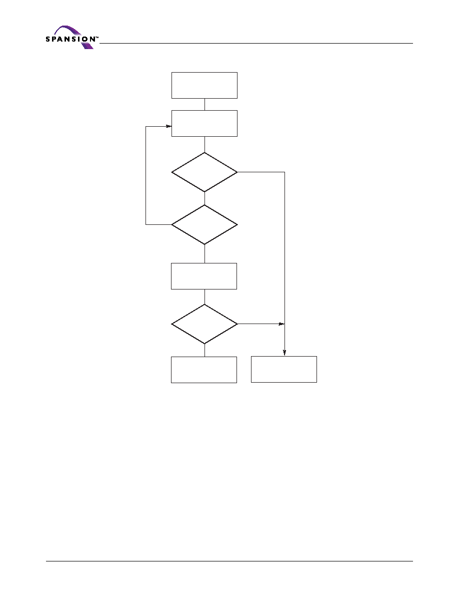
28
S29AL008D
S29AL008D_00A3 June 16, 2005
D a t a S h e e t
RY/BY#: Ready/Busy#
The RY/BY# is a dedicated, open-drain output pin that indicates whether an Em-
bedded Algorithm is in progress or complete. The RY/BY# status is valid after the
rising edge of the final WE# pulse in the command sequence. Since RY/BY# is an
open-drain output, several RY/BY# pins can be tied together in parallel with a
pull-up resistor to V
CC
.
DQ7 = Data?
Yes
No
No
DQ5 = 1?
No
Yes
Yes
FAIL
PASS
Read DQ7≠DQ0
Addr = VA
Read DQ7≠DQ0
Addr = VA
DQ7 = Data?
START
Notes:
1. VA = Valid address for programming. During a sector
erase operation, a valid address is an address within
any sector selected for erasure. During chip erase, a
valid address is any non-protected sector address.
2. DQ7 should be rechecked even if DQ5 = 1 because
DQ7 may change simultaneously with DQ5.
Figure 5. Data# Polling Algorithm

June 16, 2005 S29AL008D_00A3
S29AL008D
29
D a t a S h e e t
If the output is low (Busy), the device is actively erasing or programming. (This
includes programming in the Erase Suspend mode.) If the output is high (Ready),
the device is ready to read array data (including during the Erase Suspend
mode), or is in the standby mode.
Table 6, on page 32
shows the outputs for RY/BY#.
Figure 13, on page 38
,
Figure
14
,
Figure 17, on page 43
and
Figure 18, on page 44
shows RY/BY# for read,
reset, program, and erase operations, respectively.
DQ6: Toggle Bit I
Toggle Bit I on DQ6 indicates whether an Embedded Program or Erase algorithm
is in progress or complete, or whether the device entered the Erase Suspend
mode. Toggle Bit I may be read at any address, and is valid after the rising edge
of the final WE# pulse in the command sequence (prior to the program or erase
operation), and during the sector erase time-out.
During an Embedded Program or Erase algorithm operation, successive read cy-
cles to any address cause DQ6 to toggle. (The system may use either OE# or CE#
to control the read cycles.) When the operation is complete, DQ6 stops toggling.
After an erase command sequence is written, if all sectors selected for erasing
are protected, DQ6 toggles for approximately 100 µs, then returns to reading
array data. If not all selected sectors are protected, the Embedded Erase algo-
rithm erases the unprotected sectors, and ignores the selected sectors that are
protected.
The system can use DQ6 and DQ2 together to determine whether a sector is ac-
tively erasing or is erase-suspended. When the device is actively erasing (that is,
the Embedded Erase algorithm is in progress), DQ6 toggles. When the device en-
ters the Erase Suspend mode, DQ6 stops toggling. However, the system must
also use DQ2 to determine which sectors are erasing or erase-suspended. Alter-
natively, the system can use DQ7 (see the subsection
DQ7: Data# Polling, on
page 27
).
If a program address falls within a protected sector, DQ6 toggles for approxi-
mately 1 µs after the program command sequence is written, then returns to
reading array data.
DQ6 also toggles during the erase-suspend-program mode, and stops toggling
once the Embedded Program algorithm is complete.
Table 6, on page 32
shows the outputs for Toggle Bit I on DQ6.
Figure 6, on page
31
shows the toggle bit algorithm.
Figure 20, on page 45
shows the toggle bit
timing diagrams.
Figure 21, on page 46
shows the differences between DQ2 and
DQ6 in graphical form. See also the subsection
DQ2: Toggle Bit II, on page 29
.
DQ2: Toggle Bit II
The Toggle Bit II on DQ2, when used with DQ6, indicates whether a particular
sector is actively erasing (that is, the Embedded Erase algorithm is in progress),
or whether that sector is erase-suspended. Toggle Bit II is valid after the rising
edge of the final WE# pulse in the command sequence.
DQ2 toggles when the system reads at addresses within those sectors that were
selected for erasure. (The system may use either OE# or CE# to control the read
cycles.) But DQ2 cannot distinguish whether the sector is actively erasing or is
erase-suspended. DQ6, by comparison, indicates whether the device is actively
erasing, or is in Erase Suspend, but cannot distinguish which sectors are selected

30
S29AL008D
S29AL008D_00A3 June 16, 2005
D a t a S h e e t
for erasure. Thus, both status bits are required for sector and mode information.
Refer to
Table 6, on page 32
to compare outputs for DQ2 and DQ6.
Figure 6, on page 31
shows the toggle bit algorithm in flowchart form, and the
section "DQ2: Toggle Bit II" explains the algorithm. See also the
DQ6: Toggle Bit
I, on page 29
subsection.
Figure 20, on page 45
shows the toggle bit timing dia-
gram.
Figure 21, on page 46
shows the differences between DQ2 and DQ6 in
graphical form.
Reading Toggle Bits DQ6/DQ2
Refer to
Figure 6, on page 31
for the following discussion. Whenever the system
initially begins reading toggle bit status, it must read DQ7≠DQ0 at least twice in
a row to determine whether a toggle bit is toggling. Typically, the system would
note and store the value of the toggle bit after the first read. After the second
read, the system would compare the new value of the toggle bit with the first. If
the toggle bit is not toggling, the device completed the program or erase opera-
tion. The system can read array data on DQ7≠DQ0 on the following read cycle.
However, if after the initial two read cycles, the system determines that the toggle
bit is still toggling, the system also should note whether the value of DQ5 is high
(see the section on DQ5). If it is, the system should then determine again
whether the toggle bit is toggling, since the toggle bit may have stopped toggling
just as DQ5 went high. If the toggle bit is no longer toggling, the device success-
fully completed the program or erase operation. If it is still toggling, the device
did not completed the operation successfully, and the system must write the reset
command to return to reading array data.
The remaining scenario is that the system initially determines that the toggle bit
is toggling and DQ5 has not gone high. The system may continue to monitor the
toggle bit and DQ5 through successive read cycles, determining the status as de-
scribed in the previous paragraph. Alternatively, it may choose to perform other
system tasks. In this case, the system must start at the beginning of the algo-
rithm when it returns to determine the status of the operation (top of
Figure 6,
on page 31
).
DQ5: Exceeded Timing Limits
DQ5 indicates whether the program or erase time exceeded a specified internal
pulse count limit. Under these conditions DQ5 produces a 1. This is a failure con-
dition that indicates the program or erase cycle was not successfully completed.
The DQ5 failure condition may appear if the system tries to program a 1 to a lo-
cation that is previously programmed to 0. Only an erase operation can
change a 0 back to a 1. Under this condition, the device halts the operation,
and when the operation exceeds the timing limits, DQ5 produces a 1.
Under both these conditions, the system must issue the reset command to return
the device to reading array data.
DQ3: Sector Erase Timer
After writing a sector erase command sequence, the system may read DQ3 to de-
termine whether or not an erase operation started. (The sector erase timer does
not apply to the chip erase command.) If additional sectors are selected for era-
sure, the entire time-out also applies after each additional sector erase
command. When the time-out is complete, DQ3 switches from 0 to 1. The system
may ignore DQ3 if the system can guarantee that the time between additional
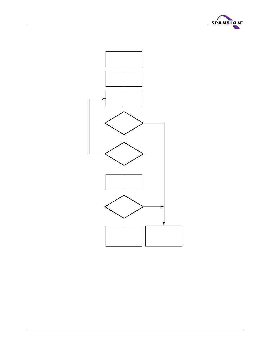
June 16, 2005 S29AL008D_00A3
S29AL008D
31
D a t a S h e e t
sector erase commands is always less than 50 µs. See also the
Sector Erase
Command Sequence, on page 23
.
After the sector erase command sequence is written, the system should read the
status on DQ7 (Data# Polling) or DQ6 (Toggle Bit I) to ensure the device accepted
the command sequence, and then read DQ3. If DQ3 is 1, the internally controlled
erase cycle started; all further commands (other than Erase Suspend) are ig-
nored until the erase operation is complete. If DQ3 is 0, the device accepts
START
No
Yes
Yes
DQ5 = 1?
No
Yes
Toggle Bit
= Toggle?
No
Program/Erase
Operation Not
Complete, Write
Reset Command
Program/Erase
Operation Complete
Read DQ7≠DQ0
Toggle Bit
= Toggle?
Read DQ7≠DQ0
Twice
Read DQ7≠DQ0
(Notes
1, 2)
Notes:
1. Read toggle bit twice to determine whether or not it
is toggling. See text.
2. Recheck toggle bit because it may stop toggling as
DQ5 changes to 1. See text.
Figure 6. Toggle Bit Algorithm
Note 1
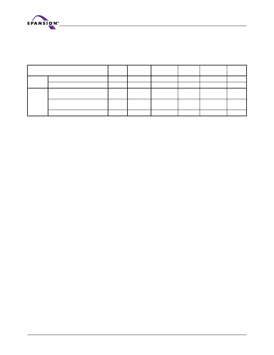
32
S29AL008D
S29AL008D_00A3 June 16, 2005
D a t a S h e e t
additional sector erase commands. To ensure the command is accepted, the sys-
tem software should check the status of DQ3 prior to and following each
subsequent sector erase command. If DQ3 is high on the second status check,
the last command might not be accepted.
Table 6
shows the outputs for DQ3.
Notes:
1. DQ5 switches to 1 when an Embedded Program or Embedded Erase operation exceeds the maximum timing limits.
See
DQ5: Exceeded Timing Limits, on page 30
for more information.
2. DQ7 and DQ2 require a valid address when reading status information. Refer to the appropriate subsection for further
details.
Table 6. Write Operation Status
Operation
DQ7
(
Note 2
)
DQ6
DQ5
(
Note 1
)
DQ3
DQ2
(
Note 2
)
RY/BY#
Standard
Mode
Embedded Program Algorithm
DQ7#
Toggle
0
N/A
No toggle
0
Embedded Erase Algorithm
0
Toggle
0
1
Toggle
0
Erase
Suspend
Mode
Reading within Erase
Suspended Sector
1
No toggle
0
N/A
Toggle
1
Reading within Non-Erase
Suspended Sector
Data
Data
Data
Data
Data
1
Erase-Suspend-Program
DQ7#
Toggle
0
N/A
N/A
0
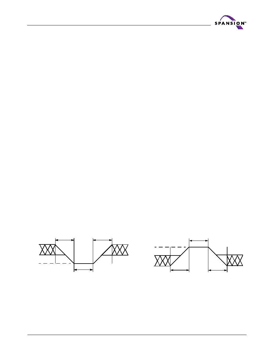
June 16, 2005 S29AL008D_00A3
S29AL008D
33
D a t a S h e e t
Absolute Maximum Ratings
Storage Temperature Plastic Packages . . . . . . . . . . . . . . . . .≠65∞C to +150∞C
Ambient Temperature with Power Applied . . . . . . . . . . . . . . .≠65∞C to +125∞C
Voltage with Respect to Ground V
CC
(
Note 1
) . . . . . . . . . . . .≠0.5 V to +4.0 V
A9, OE#, and RESET# (
Note 2
) . . . . . . . . . . . . . . . . . . . . . ≠0.5 V to +12.5 V
All other pins (
Note 1
) . . . . . . . . . . . . . . . . . . . . . . . . . ≠0.5 V to V
CC
+0.5 V
Output Short Circuit Current (
Note 3
). . . . . . . . . . . . . . . . . . . . . . . . 200 mA
Notes:
1. Minimum DC voltage on input or I/O pins is ≠0.5 V. During voltage transitions, input or I/O pins may undershoot V
SS
to ≠2.0 V for periods of up to 20 ns. See
Figure 7, on page 33
. Maximum DC voltage on input or I/O pins is V
CC
+0.5
V. During voltage transitions, input or I/O pins may overshoot to V
CC
+2.0 V for periods up to 20 ns. See
Figure 8,
on page 33
.
2. Minimum DC input voltage on pins A9, OE#, and RESET# is ≠0.5 V. During voltage transitions, A9, OE#, and
RESET# may undershoot V
SS
to ≠2.0 V for periods of up to 20 ns. See
Figure 7, on page 33
. Maximum DC input
voltage on pin A9 is +12.5 V which may overshoot to 14.0 V for periods up to 20 ns.
3. No more than one output may be shorted to ground at a time. Duration of the short circuit should not be greater
than one second.
Stresses above those listed under "Absolute Maximum Ratings" may cause permanent damage to the device. This is a stress
rating only; functional operation of the device at these or any other conditions above those indicated in the operational sections
of this data sheet is not implied. Exposure of the device to absolute maximum rating conditions for extended periods may
affect device reliability.
Operating Ranges
Industrial (I) Devices
Ambient Temperature (T
A
) . . . . . . . . . . . . . . . . . . . . . . . . . -40∞C to +85∞C
Extended (N) Devices
Ambient Temperature (T
A
) . . . . . . . . . . . . . . . . . . . . . . . . -40∞C to +125∞C
V
CC
Supply Voltages
V
CC
for regulated voltage range . . . . . . . . . . . . . . . . . . . . . +3.0 V to +3.6 V
V
CC
for full voltage range . . . . . . . . . . . . . . . . . . . . . . . . . +2.7 V to +3.6 V
Operating ranges define those limits between which the functionality of the device is guaranteed
Figure 7. Maximum Negative Overshoot Waveform Figure 8. Maximum Positive Overshoot Waveform
20 ns
20 ns
20 ns
+0.8 V
≠0.5 V
≠2.0 V
20 ns
20 ns
20 ns
V
CC
+2.0 V
V
CC
+0.5 V
2.0 V
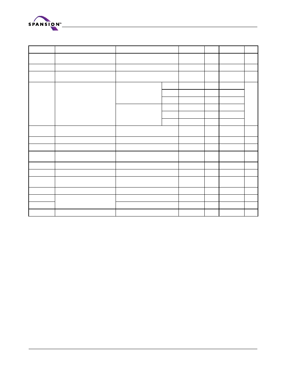
34
S29AL008D
S29AL008D_00A3 June 16, 2005
D a t a S h e e t
DC Characteristics
Notes:
1. The I
CC
current listed is typically less than 2 mA/MHz, with OE# at V
IH
. Typical V
CC
is 3.0 V.
2. Maximum I
CC
specifications are tested with V
CC
= V
CCmax
.
3. I
CC
active while Embedded Erase or Embedded Program is in progress.
4. At extended temperature range (>+85∞C), typical current is 5µA and maximum current is 10µA.
5. Automatic sleep mode enables the low power mode when addresses remain stable for t
ACC
+ 30 ns.
6. Not 100% tested.
Parameter
Description
Test Conditions
Min
Typ
Max
Unit
I
LI
Input Load Current
V
IN
= V
SS
to V
CC
,
V
CC
= V
CC
max
±1.0
µA
I
LIT
A9 Input Load Current
V
CC
= V
CC max
; A9 = 12.5 V
35
µA
I
LO
Output Leakage Current
V
OUT
= V
SS
to V
CC
,
V
CC
= V
CC max
±1.0
µA
I
CC1
V
CC
Active Read Current
(Notes
1
,
2
)
CE# = V
IL,
OE#
=
V
IH,
Byte Mode
10 MHz
15
30
mA
5 MHz
9
16
1 MHz
2
4
CE# = V
IL,
OE#
=
V
IH,
Word Mode
10 MHz
15
30
5 MHz
9
16
1 MHz
2
4
I
CC2
V
CC
Active Write Current
(Notes
2
,
3
,
6
)
CE# = V
IL,
OE#
=
V
IH
20
35
mA
I
CC3
V
CC
Standby Current (Notes
2
,
4
)
CE#, RESET# = V
CC
±0.3 V
0.2
5
µA
I
CC4
V
CC
Reset Current (Notes
2
,
4
)
RESET# = V
SS
± 0.3 V
0.2
5
µA
I
CC5
Automatic Sleep Mode
(Notes
2
,
4
,
5
)
V
IH
= V
CC
± 0.3 V;
V
IL
= V
SS
± 0.3 V
0.2
5
µA
V
IL
Input Low Voltage
≠0.5
0.8
V
V
IH
Input High Voltage
0.7 x V
CC
V
CC
+ 0.3
V
V
ID
Voltage for Autoselect and
Temporary Sector Unprotect
V
CC
= 3.3 V
11.5
12.5
V
V
OL
Output Low Voltage
I
OL
= 4.0 mA, V
CC
= V
CC min
0.45
V
V
OH1
Output High Voltage
I
OH
= ≠2.0 mA, V
CC
= V
CC min
2.4
V
V
OH2
I
OH
= ≠100 µA, V
CC
= V
CC min
V
CC
≠0.4
V
LKO
Low V
CC
Lock-Out Voltage
2.3
2.5
V
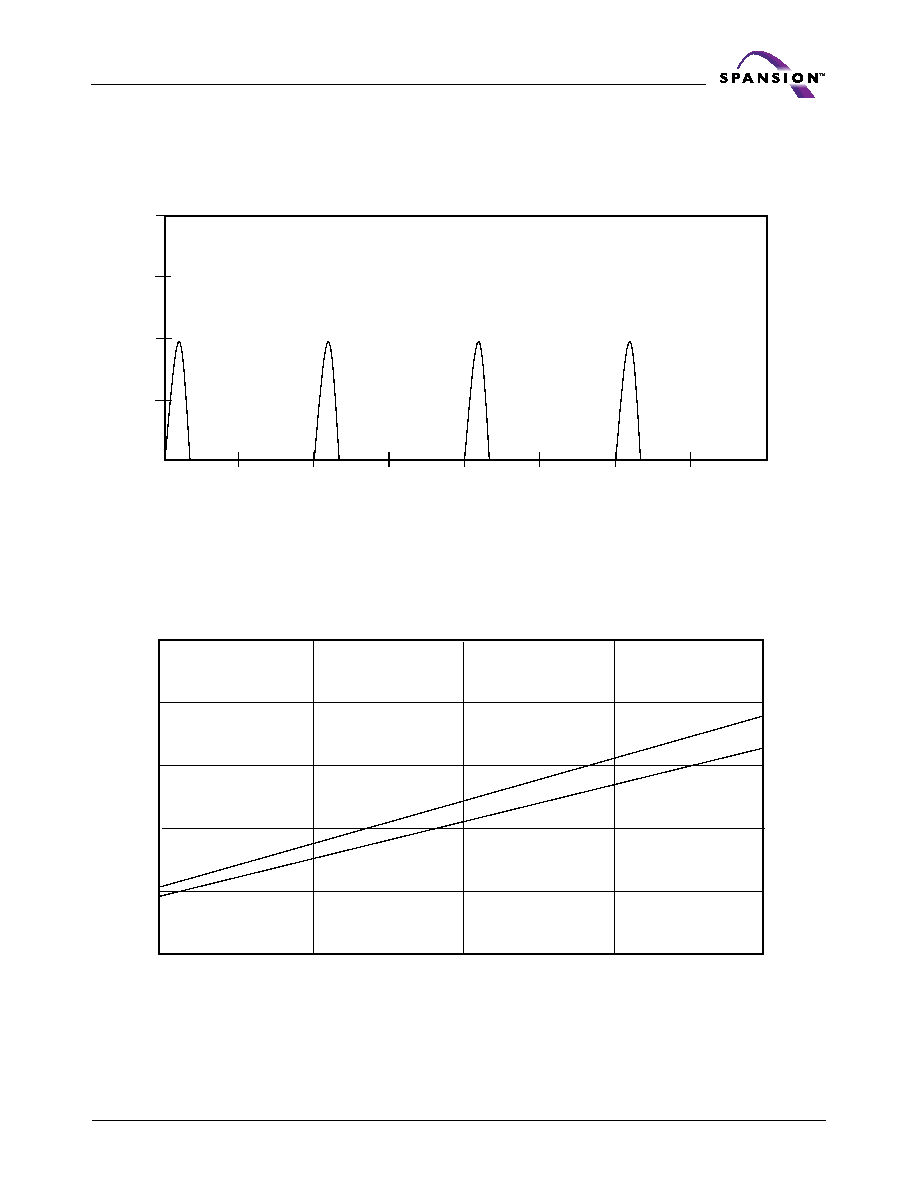
June 16, 2005 S29AL008D_00A3
S29AL008D
35
D a t a S h e e t
DC Characteristics (Continued)
Zero Power Flash
20
15
10
5
0
0
500
1000
1500
2000
2500
3000
3500
4000
S
upp
l
y
C
u
rr
ent i
n
m
A
Time in ns
Note: Addresses are switching at 1 MHz
Figure 9. I
CC1
Current vs. Time (Showing Active and Automatic Sleep Currents)
10
8
2
0
1
2
3
4
5
Frequency in MHz
S
u
pp
l
y
C
u
r
r
e
nt
i
n
mA
Note: T = 25 ∞C
Figure 10. Typical I
CC1
vs. Frequency
2.7 V
3.6 V
4
6

36
S29AL008D
S29AL008D_00A3 June 16, 2005
D a t a S h e e t
Test Conditions
Note: Nodes are IN3064 or equivalent.
Figure 11. Test Setup
Table 7. Test Specifications
Test Condition
55
70
90
Unit
Output Load
1 TTL gate
Output Load Capacitance, C
L
(including jig capacitance)
30
30
100
pF
Input Rise and Fall Times
5
ns
Input Pulse Levels
0.0≠3.0
V
Input timing measurement reference levels
1.5
Output timing measurement reference levels
1.5
2.7 k
CL
6.2 k
3.3 V
Device
Under
Test
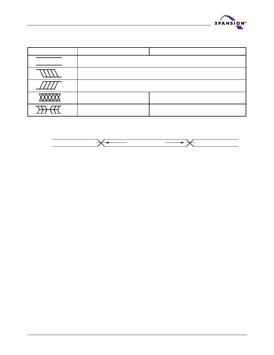
June 16, 2005 S29AL008D_00A3
S29AL008D
37
D a t a S h e e t
Key to Switching Waveforms
WAVEFORM
INPUTS
OUTPUTS
Steady
Changing from H to L
Changing from L to H
Don't Care, Any Change Permitted
Changing, State Unknown
Does Not Apply
Center Line is High Impedance State (High Z)
3.0 V
0.0 V
1.5 V
1.5 V
Output
Measurement Level
Input
Figure 12. Input Waveforms and Measurement Levels

38
S29AL008D
S29AL008D_00A3 June 16, 2005
D a t a S h e e t
AC Characteristics
Notes:
1. Not 100% tested.
2. See
Figure 11, on page 36
and
DC Characteristics, on page 34
for test specifications.
Table 8. Read Operations
Parameter
Description
Speed Options
JEDEC
Std
Test Setup
55
70
90
Unit
t
AVAV
t
RC
Read Cycle Time (
Note 1
)
Min
55
70
90
ns
t
AVQV
t
ACC
Address to Output Delay
CE# = V
IL
OE# = V
IL
Max
55
70
90
t
ELQV
t
CE
Chip Enable to Output Delay
OE# = V
IL
Max
55
70
90
t
GLQV
t
OE
Output Enable to Output Delay
Max
25
30
35
t
EHQZ
t
DF
Chip Enable to Output High Z (
Note 1
)
Max
25
25
30
t
GHQZ
t
DF
Output Enable to Output High Z (
Note 1
)
Max
25
25
30
t
OEH
Output Enable
Hold Time (
Note 1
)
Read
Min
0
Toggle and
Data# Polling
Min
10
t
AXQX
t
OH
Output Hold Time From Addresses, CE# or OE#,
Whichever Occurs First (
Note 1
)
Min
0
tCE
Outputs
WE#
Addresses
CE#
OE#
HIGH Z
Output Valid
HIGH Z
Addresses Stable
tRC
tACC
tOEH
tO
0 V
RY/BY#
RESET#
tD
tO
Figure 13. Read Operations Timings
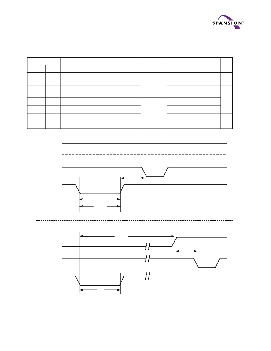
June 16, 2005 S29AL008D_00A3
S29AL008D
39
D a t a S h e e t
AC Characteristics
Note: Not 100% tested.
Table 9. Hardware Reset (RESET#)
Parameter
Description
All Speed Options
JEDEC
Std
Test Setup
Unit
t
READY
RESET# Pin Low (During Embedded
Algorithms) to Read or Write (See
Note
)
Max
20
µs
t
READY
RESET# Pin Low (NOT During Embedded
Algorithms) to Read or Write (See
Note
)
500
ns
t
RP
RESET# Pulse Width
Min
500
t
RH
RESET# High Time Before Read (See
Note
)
50
t
RPD
RESET# Low to Standby Mode
20
µs
t
RB
RY/BY# Recovery Time
0
ns
RESET#
RY/BY#
RY/BY#
tRP
tReady
Reset Timings NOT during Embedded Algorithms
tReady
CE#, OE#
tRH
CE#, OE#
Reset Timings during Embedded Algorithms
RESET#
tRP
tRB
Figure 14. RESET# Timings
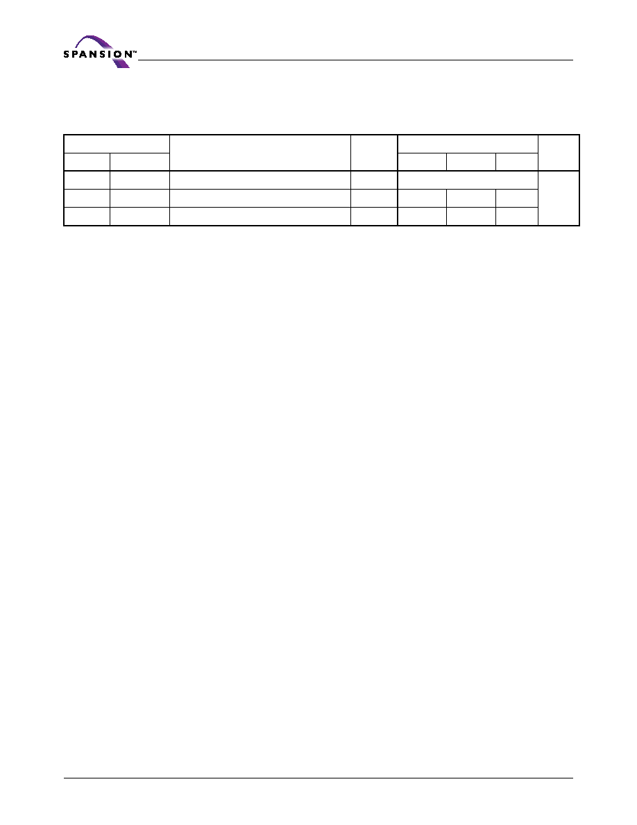
40
S29AL008D
S29AL008D_00A3 June 16, 2005
D a t a S h e e t
AC Characteristics
Table 10. Word/Byte Configuration (BYTE#)
Parameter
Speed Options
JEDEC
Std
Description
55
70
90
Unit
t
ELFL/
t
ELFH
CE# to BYTE# Switching Low or High
Max
5
ns
t
FLQZ
BYTE# Switching Low to Output HIGH Z
Max
25
25
30
t
FHQV
BYTE# Switching High to Output Active
Min
55
70
90
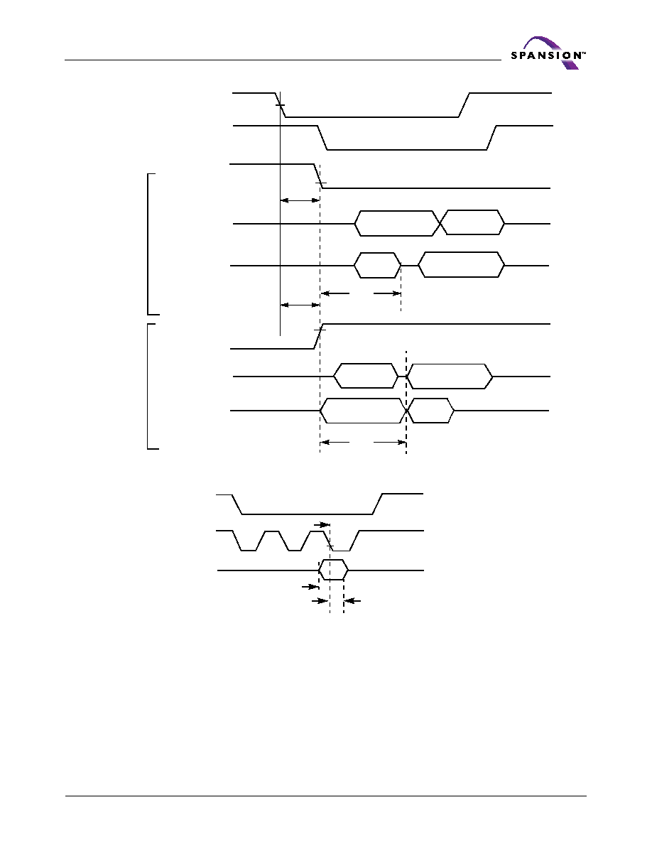
June 16, 2005 S29AL008D_00A3
S29AL008D
41
D a t a S h e e t
DQ15
Output
Data Output
(DQ0≠DQ7)
CE#
OE#
BYTE#
t
ELFL
DQ0≠DQ14
Data Output
(DQ0≠DQ14)
DQ15/A-1
Address
Input
t
FLQZ
BYTE#
Switching
from word
to byte
mode
DQ15
Output
Data Output
(DQ0≠DQ7)
BYTE#
t
ELFH
DQ0≠DQ14
Data Output
(DQ0≠DQ14)
DQ15/A-1
Address
Input
t
FHQV
BYTE#
Switching
from byte
to word
mode
Figure 15. BYTE# Timings for Read Operations
Note:
Refer to the Erase/Program Operations table for t
AS
and t
AH
specifications.
Figure 16. BYTE# Timings for Write Operations
CE#
WE#
BYTE#
The falling edge of the last WE# signal
t
HOLD
(t
AH
)
t
SET
(t
AS
)
42
S29AL008D
S29AL008D_00A3 June 16, 2005
D a t a S h e e t
AC Characteristics
Erase / Program Operations
Notes:
1. Not 100% tested.
2. See
Table , on page 49
for more information.
Parameter
Speed Options
JEDEC
Std
Description
55
70
90
Unit
t
AVAV
t
WC
Write Cycle Time (
Note 1
)
Min
55
70
90
ns
t
AVWL
t
AS
Address Setup Time
0
t
WLAX
t
AH
Address Hold Time
45
t
DVWH
t
DS
Data Setup Time
35
35
45
t
WHDX
t
DH
Data Hold Time
0
t
OES
Output Enable Setup Time
0
t
GHWL
t
GHWL
Read Recovery Time Before Write
(OE# High to WE# Low)
0
t
ELWL
t
CS
CE# Setup Time
0
t
WHEH
t
CH
CE# Hold Time
0
t
WLWH
t
WP
Write Pulse Width
35
t
WHWL
t
WPH
Write Pulse Width High
30
t
WHWH1
t
WHWH1
Programming Operation (
Note 2
)
Byte
Typ
5
µs
Word
7
t
WHWH2
t
WHWH2
Sector Erase Operation (
Note 2
)
0.7
sec
t
VCS
V
CC
Setup Time (
Note 1
)
Min
50
µs
t
RB
Recovery Time from RY/BY#
0
ns
t
BUSY
Program/Erase Valid to RY/BY# Delay
90
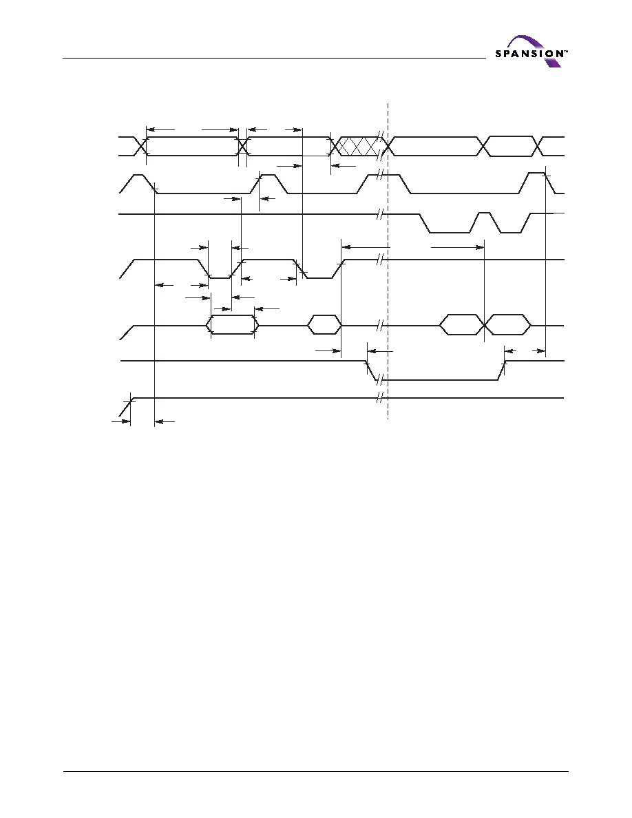
June 16, 2005 S29AL008D_00A3
S29AL008D
43
D a t a S h e e t
AC Characteristics
OE#
WE#
CE#
VCC
Data
Addresses
tD
tAH
tD
tW
PD
tWHWH1
tWC
tAS
tWPH
tVCS
555h
PA
PA
Read Status Data (last two cycles)
A0h
tCS
Statu
DOUT
Program Command Sequence (last two cycles)
RY/BY#
tRB
tBUSY
tC
PA
Notes:
1. PA = program address, PD = program data, D
OUT
is the true data at the program address.
2. Illustration shows device in word mode.
Figure 17. Program Operation Timings

44
S29AL008D
S29AL008D_00A3 June 16, 2005
D a t a S h e e t
AC Characteristics
OE#
CE#
Addresses
VCC
WE#
Data
2AAh
SA
tA
tW
tWC
tAS
tWP
555h for chip erase
10 for Chip Erase
30h
tD
tVC
tCS
tD
55h
tC
In
Progress Complete
tWHWH
VA
VA
Erase Command Sequence (last two cycles)
Read Status Data
RY/BY#
tRB
tBUSY
Notes:
1. SA = sector address (for Sector Erase), VA = Valid Address for reading status data (see
Write Operation Status, on
page 27
).
2. Illustration shows device in word mode.
Figure 18. Chip/Sector Erase Operation Timings
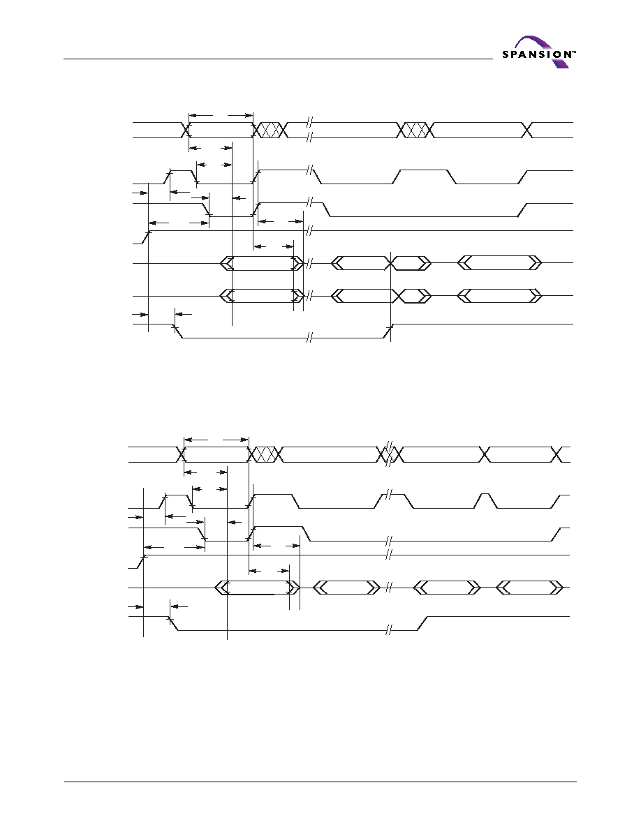
June 16, 2005 S29AL008D_00A3
S29AL008D
45
D a t a S h e e t
AC Characteristics
WE#
CE#
OE#
High
tOE
High
DQ7
DQ0≠DQ6
RY/BY#
tBUS
Compleme
Tru
Addresses
VA
tOEH
tCE
tCH
tOH
tDF
VA
VA
Status
Complement
Status
Tru
Valid Data
Valid Data
tACC
tRC
Note:
VA = Valid address. Illustration shows first status cycle after command sequence, last status read cycle, and array
data read cycle.
Figure 19. Data# Polling Timings (During Embedded Algorithms)
WE#
CE#
OE#
High
tOE
DQ6/DQ2
RY/BY#
tBUS
Addresses
VA
tOEH
tCE
tCH
tOH
tDF
VA
VA
tACC
tRC
Valid Data
Valid
Valid
(first read)
(second read)
(stops toggling)
Valid
VA
Note:
VA = Valid address; not required for DQ6. Illustration shows first two status cycle after command sequence, last status
read cycle, and array data read cycle.
Figure 20. Toggle Bit Timings (During Embedded Algorithms)

46
S29AL008D
S29AL008D_00A3 June 16, 2005
D a t a S h e e t
AC Characteristics
Note: Not 100% tested.
Table 11. Temporary Sector Unprotect
Parameter
All Speed Options
JEDEC
Std
Description
Unit
t
VIDR
V
ID
Rise and Fall Time (See Note)
Min
500
ns
t
RSP
RESET# Setup Time for Temporary Sector
Unprotect
Min
4
µs
Note:
The system may use CE# or OE# to toggle DQ2 and DQ6. DQ2 toggles only when read at an address within an
erase-suspended sector.
Figure 21. DQ2 vs. DQ6
Enter
Erase
Erase
Erase
Enter Erase
Suspend Program
Erase Suspend
Read
Erase Suspend
Read
Erase
WE#
DQ6
DQ2
Erase
Complete
Erase
Suspend
Suspend
Program
Resume
Embedded
Erasing
RESET#
tVIDR
12 V
0 or 3 V
CE#
WE#
RY/BY#
tVIDR
tRSP
Program or Erase Command Sequence
0 or 3 V
Figure 22. Temporary Sector Unprotect Timing Diagram
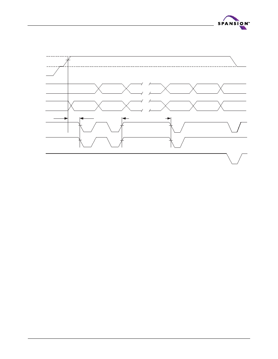
June 16, 2005 S29AL008D_00A3
S29AL008D
47
D a t a S h e e t
AC Characteristics
Sector Protect: 150 s
Sector Unprotect: 15 ms
1 s
RESET#
SA, A6,
A1, A0
Data
CE#
WE#
OE#
60h
60h
40h
Valid*
Valid*
Valid*
Status
Sector Protect/Unprotect
Verify
VID
VIH
* For sector protect, A6 = 0, A1 = 1, A0 = 0. For sector unprotect, A6 = 1, A1 = 1, A0 = 0.
Figure 23. Sector Protect/Unprotect Timing Diagram
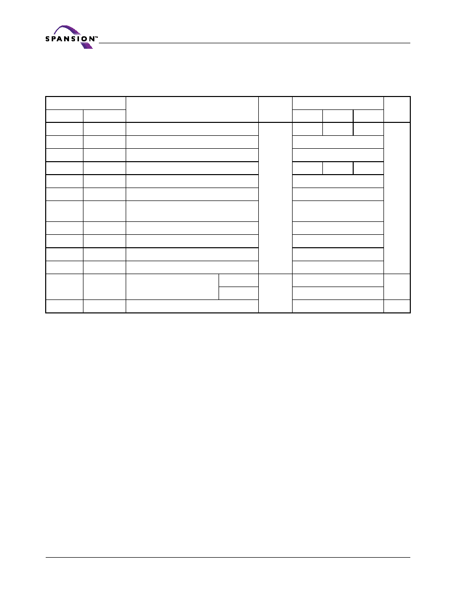
48
S29AL008D
S29AL008D_00A3 June 16, 2005
D a t a S h e e t
AC Characteristics
Notes:
1. Not 100% tested.
2. See
Table , on page 49
for more information.
Table 12. Alternate CE# Controlled Erase/Program Operations
Parameter
Speed Options
JEDEC
Std
Description
55
70
90
Unit
t
AVAV
t
WC
Write Cycle Time (
Note 1
)
Min
55
70
90
ns
t
AVEL
t
AS
Address Setup Time
0
t
ELAX
t
AH
Address Hold Time
45
t
DVEH
t
DS
Data Setup Time
35
35
45
t
EHDX
t
DH
Data Hold Time
0
t
OES
Output Enable Setup Time
0
t
GHEL
t
GHEL
Read Recovery Time Before Write
(OE# High to WE# Low)
0
t
WLEL
t
WS
WE# Setup Time
0
t
EHWH
t
WH
WE# Hold Time
0
t
ELEH
t
CP
CE# Pulse Width
35
t
EHEL
t
CPH
CE# Pulse Width High
30
t
WHWH1
t
WHWH1
Programming Operation
(
Note 2
)
Byte
Typ
8
µs
Word
16
t
WHWH2
t
WHWH2
Sector Erase Operation (
Note 2
)
1
sec
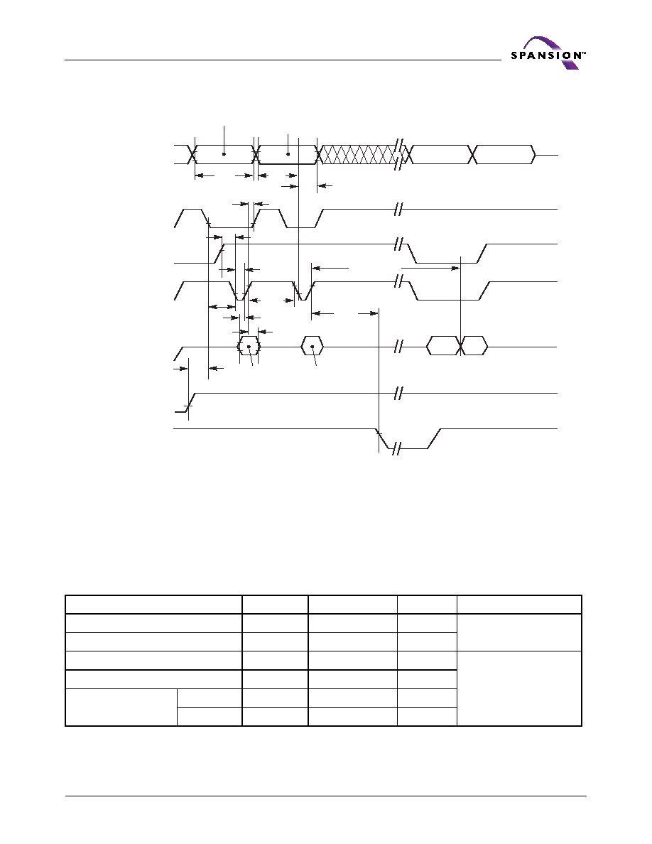
June 16, 2005 S29AL008D_00A3
S29AL008D
49
D a t a S h e e t
AC Characteristics
Notes:
1. Typical program and erase times assume the following conditions: 25
∞
C, 3.0 V V
CC
, 1,000,000 cycles. Additionally,
programming typicals assume checkerboard pattern.
Erase and Programming Performance
Parameter
Typ
Note 1
Max
Note 2
Unit
Comments
Sector Erase Time
0.7
10
s
Excludes 00h programming
prior to erasure
Chip Erase Time
14
s
Byte Programming Time
7
210
µs
Excludes system level
overhead
Note 5
Word Programming Time
7
210
µs
Chip Programming Time
Note 3
Byte Mode
8.4
25
s
Word Mode
5.8
17
s
tGHEL
tWS
OE#
CE#
WE#
RESET#
tD
Data
tAH
Addresses
tD
tCP
DQ7
D
OUT
tWC
tAS
tCPH
PA
Data# Polling
A0 for program
55 for erase
tR
tWHWH1 or
RY/BY#
tWH
PD for program
30 for sector erase
10 for chip erase
555 for program
2AA for erase
PA for program
SA for sector erase
555 for chip erase
tBUS
Notes:
1. PA = program address, PD = program data, DQ7# = complement of the data written to the device, D
OUT
= data
written to the device.
2. Figure indicates the last two bus cycles of command sequence.
3. Word mode address used as an example.
Figure 24. Alternate CE# Controlled Write Operation Timings
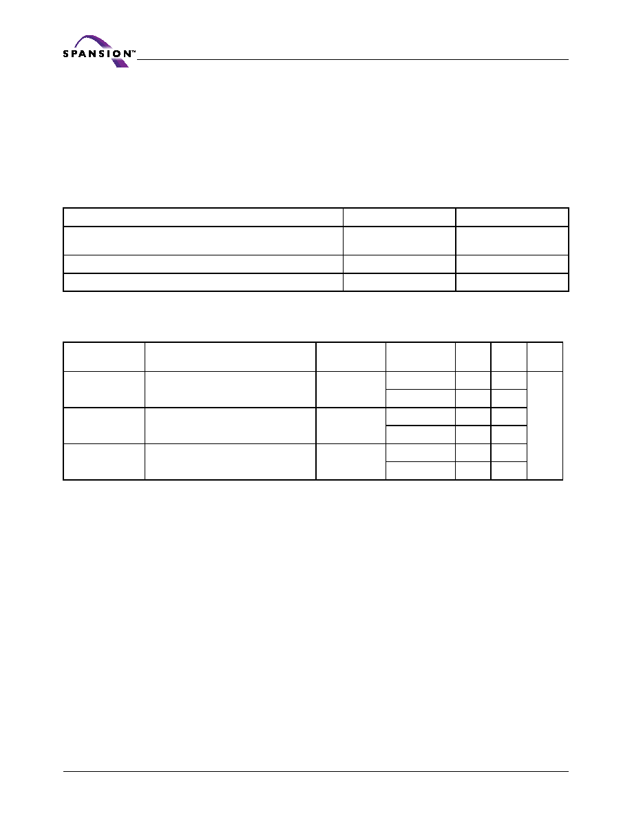
50
S29AL008D
S29AL008D_00A3 June 16, 2005
D a t a S h e e t
2. Under worst case conditions of 90∞C, V
CC
= 2.7 V, 1,000,000 cycles.
3. The typical chip programming time is considerably less than the maximum chip programming time listed, since most
bytes program faster than the maximum program times listed.
4. In the pre-programming step of the Embedded Erase algorithm, all bytes are programmed to 00h before erasure.
5. System-level overhead is the time required to execute the two- or four-bus-cycle sequence for the program
command. See
Table 5, on page 25
for further information on command definitions.
6. The device has a guaranteed minimum erase and program cycle endurance of 1,000,000 cycles.
Includes all pins except V
CC
. Test conditions: V
CC
= 3.0 V, one pin at a time.
Notes:
1. Sampled, not 100% tested.
2. Test conditions T
A
= 25∞C, f = 1.0 MHz.
Table 13. Latchup Characteristics
Description
Min
Max
Input voltage with respect to V
SS
on all pins except I/O pins
(including A9, OE#, and RESET#)
≠1.0 V
12.5 V
Input voltage with respect to V
SS
on all I/O pins
≠1.0 V
V
CC
+ 1.0 V
V
CC
Current
≠100 mA
+100 mA
Table 14. TSOP, SO, and BGA Pin Capacitance
Parameter
Symbol
Parameter Description
Test Setup
Package
Typ
Max
Unit
C
IN
Input Capacitance
V
IN
= 0
TSOP, SO
6
7.5
pF
BGA
4.2
5.0
C
OUT
Output Capacitance
V
OUT
= 0
TSOP, SO
8.5
12
BGA
5.4
6.5
C
IN2
Control Pin Capacitance
V
IN
= 0
TSOP, SO
7.5
9
BGA
3.9
4.7
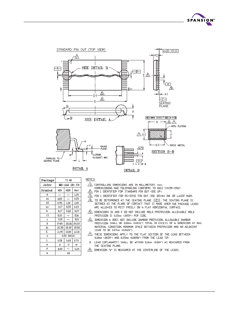
June 16, 2005 S29AL008D_00A3
S29AL008D
51
D a t a S h e e t
Physical Dimensions
TS 048--48-Pin Standard TSOP
* For reference only. BSC is an ANSI standard for Basic Space Centering.
Dwg rev AA; 10/99
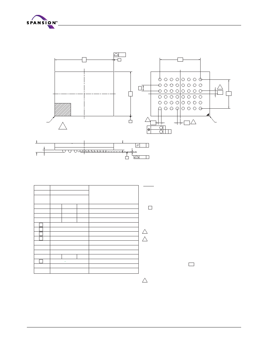
52
S29AL008D
S29AL008D_00A3 June 16, 2005
D a t a S h e e t
Physical Dimensions
VBK 048 - 48 Ball Fine-Pitch Ball Grid Array (FBGA) 8.15 x 6.15 mm
3338 \ 16-038.25b
NOTES:
1. DIMENSIONING AND TOLERANCING PER ASME Y14.5M-1994.
2. ALL DIMENSIONS ARE IN MILLIMETERS.
3. BALL POSITION DESIGNATION PER JESD 95-1, SPP-010 (EXCEPT
AS
NOTED).
4. e REPRESENTS THE SOLDER BALL GRID PITCH.
5. SYMBOL "MD" IS THE BALL ROW MATRIX SIZE IN THE
"D"
DIRECTION.
SYMBOL "ME" IS THE BALL COLUMN MATRIX SIZE IN THE
"E"
DIRECTION.
N IS THE TOTAL NUMBER OF SOLDER BALLS.
6 DIMENSION "b" IS MEASURED AT THE MAXIMUM BALL
DIAMETER IN A PLANE PARALLEL TO DATUM C.
7 SD AND SE ARE MEASURED WITH RESPECT TO DATUMS
A AND B AND DEFINE THE POSITION OF THE CENTER
SOLDER BALL IN THE OUTER ROW.
WHEN THERE IS AN ODD NUMBER OF SOLDER BALLS IN
THE OUTER ROW PARALLEL TO THE D OR E DIMENSION,
RESPECTIVELY, SD OR SE = 0.000.
WHEN THERE IS AN EVEN NUMBER OF SOLDER BALLS IN
THE OUTER ROW, SD OR SE = e/2
8. NOT USED.
9. "+" INDICATES THE THEORETICAL CENTER OF DEPOPULATED
BALLS.
10 A1 CORNER TO BE IDENTIFIED BY CHAMFER, LASER OR INK
MARK, METALLIZED MARK INDENTATION OR OTHER MEANS.
PACKAGE VBK
048
JEDEC N/A
6.15 mm x 8.15 mm NOM
PACKAGE
SYMBOL MIN NOM MAX
NOTE
A
---
---
1.00 OVERALL
THICKNESS
A1
0.18
---
--- BALL
HEIGHT
A2
0.62
---
0.76 BODY
THICKNESS
D
8.15 BSC.
BODY SIZE
E
6.15 BSC.
BODY SIZE
D1
5.60 BSC.
BALL FOOTPRINT
E1
4.00 BSC.
BALL FOOTPRINT
MD
8
ROW MATRIX SIZE D DIRECTION
ME
6
ROW MATRIX SIZE E DIRECTION
N 48
TOTAL
BALL
COUNT
fb
0.35
---
0.43 BALL
DIAMETER
e
0.80 BSC.
BALL PITCH
SD / SE
0.40 BSC.
SOLDER BALL PLACEMENT
---
DEPOPULATED SOLDER BALLS
SIDE VIEW
TOP VIEW
SEATING PLANE
A2
A
(4X)
0.10
10
D
E
C
0.10
A1
C
B
A
C
0.08
BOTTOM VIEW
A1 CORNER
B
A
M
f 0.15
C
M
7
7
6
e
SE
SD
6
5
4
3
2
A
B
C
D
E
F
G
1
H
fb
E1
D1
C
f 0.08
PIN A1
CORNER
INDEX MARK
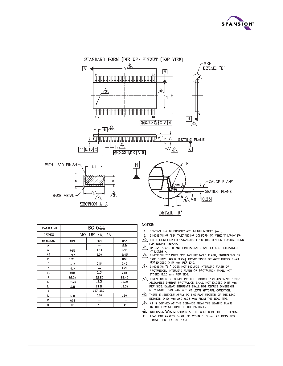
June 16, 2005 S29AL008D_00A3
S29AL008D
53
D a t a S h e e t
Physical Dimensions
SO 044--44-Pin Small Outline Package
Dwg rev AC; 10/99

54
S29AL008D
S29AL008D_00A3 June 16, 2005
D a t a S h e e t
Revision Summary
Revision A (September 8, 2004)
Initial release
Revision A 1 (February 18, 2005)
Global
Updated Trademark
Ordering Information
Added Package type designator
Valid Combinations
Changed Package Type, Material, and Temperature Range designator
Under Package Descriptions, change SSOP to SOP
Revision A2 (June 1, 2005)
Global
Updated status from Advance Information to Preliminary data sheet.
Distinctive Characteristics
Updated manufactured process technology.
Updated high performance access time.
Added extended temperature range.
Added cycling endurance information.
Production Selector Guide
Added 55ns speed option and column.
Ordering Information
Added tube and tray packing types.
Added extended temperature range
Added model numbers.
Valid Combinations Table
Added speed option.
Added packing types.
Added model number.
Added note for this table.
Operating Range
Added extended temperature range information.
Test Conditions
Added 55ns speed option.
AC Characteristics
Read Operation Table
Added 55ns speed option.
Word/Byte Configuration Table
Added 55ns speed option.

June 16, 2005 S29AL008D_00A3
S29AL008D
55
D a t a S h e e t
Erase/Program Operation Table
Added 55ns speed option.
Alternate CE# Controlled Erase/Program Operation Table
Added 55ns speed option.
Erase and Programming Performance
Changed Byte Programing Time values for Typical and Maximum.
Revision A3 (June 16, 2005)
Changed from Preliminary to full Data Sheet.
Updated Valid Combinations table.
Colophon
The products described in this document are designed, developed and manufactured as contemplated for general use, including without limitation, ordinary
industrial use, general office use, personal use, and household use, but are not designed, developed and manufactured as contemplated (1) for any use that
includes fatal risks or dangers that, unless extremely high safety is secured, could have a serious effect to the public, and could lead directly to death, personal
injury, severe physical damage or other loss (i.e., nuclear reaction control in nuclear facility, aircraft flight control, air traffic control, mass transport control,
medical life support system, missile launch control in weapon system), or (2) for any use where chance of failure is intolerable (i.e., submersible repeater and
artificial satellite). Please note that Spansion will not be liable to you and/or any third party for any claims or damages arising in connection with above-men-
tioned uses of the products. Any semiconductor devices have an inherent chance of failure. You must protect against injury, damage or loss from such failures
by incorporating safety design measures into your facility and equipment such as redundancy, fire protection, and prevention of over-current levels and other
abnormal operating conditions. If any products described in this document represent goods or technologies subject to certain restrictions on export under
the Foreign Exchange and Foreign Trade Law of Japan, the US Export Administration Regulations or the applicable laws of any other country, the prior au-
thorization by the respective government entity will be required for export of those products.
Trademarks and Notice
The contents of this document are subject to change without notice. This document may contain information on a Spansion LLC product under development
by Spansion LLC. Spansion LLC reserves the right to change or discontinue work on any product without notice. The information in this document is provided
as is without warranty or guarantee of any kind as to its accuracy, completeness, operability, fitness for particular purpose, merchantability, non-infringement
of third-party rights, or any other warranty, express, implied, or statutory. Spansion LLC assumes no liability for any damages of any kind arising out of the
use of the information in this document.
Copyright ©2004-2005 Spansion LLC. All rights reserved. Spansion, the Spansion logo, and MirrorBit are trademarks of Spansion LLC. Other company and
product names used in this publication are for identification purposes only and may be trademarks of their respective companies