
Publication Number S29AL016M_00 Revision A Amendment 4 Issue Date April 21, 2004
DATASHEET
S29AL016M
16 Megabit (2 M x 8-Bit/1 M x 16-Bit)
3.0 Volt-only Boot Sector Flash Memory
featuring MirrorBit
TM
technology
Data Sheet
Distinctive Characteristics
Architectural Advantages
Single power supply operation
-- 3 V for read, erase, and program operations
Manufactured on 0.23 µm MirrorBit
TM
process
technology
SecSi
TM
(Secured Silicon) Sector region
-- 128-word/256-byte sector for permanent, secure
identification through an 8-word/16-byte random
Electronic Serial Number, accessible through a
command sequence
-- May be programmed and locked at the factory or by
the customer
Flexible sector architecture
-- One 16 Kbyte, two 8 Kbyte, one 32 Kbyte, and thirty-
one 64 Kbyte sectors (byte mode)
-- One 8 Kword, two 4 Kword, one 16 Kword, and thirty-
one 32 Kword sectors (word mode)
Compatibility with JEDEC standards
-- Provides pinout and software compatibility for single-
power supply flash, and superior inadvertent write
protection
Top or bottom boot block configurations available
100,000 erase cycle typical per sector
20-year typical data retention
Performance Characteristics
High performance
-- 90 ns access time
-- 0.7 s typical sector erase time
Low power consumption (typical values at 5 MHz)
-- 400 nA standby mode current
-- 15 mA read current
-- 40 mA program/erase current
-- 400 nA Automatic Sleep mode current
Package options
-- 48-ball Fine-pitch BGA
-- 64-ball Fortified BGA
-- 48-pin TSOP
Software Features
-- Program Suspend & Resume: read other sectors
before programming operation is completed
-- Erase Suspend & Resume: read/program other
sectors before an erase operation is completed
-- Data# polling & toggle bits provide status
-- Unlock Bypass Program command reduces overall
multiple-word programming time
-- CFI (Common Flash Interface) compliant: allows host
system to identify and accommodate multiple flash
devices
Hardware Features
-- Sector Protection: hardware-level method of
preventing write operations within a sector
-- Temporary Sector Unprotect: V
ID
-level method of
changing code in locked sectors
-- Hardware reset input (RESET#) resets device
-- Ready/Busy# output (RY/BY#) indicates program or
erase cycle completion

3
S29AL016M
S29AL016M_00A4 April 21, 2004
General Description
The S29AL016M is a 16 Mbit, 3.0 Volt-only Flash memory organized as 2,097,152
bytes or 1,048,576 words. The device is offered in a 48-ball Fine-pitch BGA, 64-
ball Fortified BGA, and 48-pin TSOP packages. The word-wide data (x16) appears
on DQ15≠DQ0; the byte-wide (x8) data appears on DQ7≠DQ0. The device re-
quires only a single 3.0 volt power supply for both read and write functions,
designed to be programmed in-system with the standard system 3.0 volt V
CC
sup-
ply. The device can also be programmed in standard EPROM programmers.
The device offers access times of 90 and 100 ns. To eliminate bus contention the
device has separate chip enable (CE#), write enable (WE#) and output enable
(OE#) controls.
The device is entirely command set compatible with the JEDEC single-power-
supply Flash standard. Commands are written to the device using standard
microprocessor write timing. Write cycles also internally latch addresses and data
needed for the programming and erase operations.
The sector erase architecture allows memory sectors to be erased and repro-
grammed without affecting the data contents of other sectors. The device is fully
erased when shipped from the factory.
Device programming and erasure are initiated through command sequences.
Once a program or erase operation has begun, the host system need only poll
the DQ7 (Data# Polling) or DQ6 (toggle) status bits or monitor the Ready/
Busy# (RY/BY#) output to determine whether the operation is complete. To
facilitate programming, an Unlock Bypass mode reduces command sequence
overhead by requiring only two write cycles to program data instead of four.
Hardware data protection measures include a low V
CC
detector that automati-
cally inhibits write operations during power transitions. The hardware sector
protection feature disables both program and erase operations in any combina-
tion of sectors of memory. This can be achieved in-system or via programming
equipment.
The Erase Suspend/Erase Resume feature allows the host system to pause an
erase operation in a given sector to read or program any other sector and then
complete the erase operation. The Program Suspend/Program Resume fea-
ture enables the host system to pause a program operation in a given sector to
read any other sector and then complete the program operation.
The hardware RESET# pin terminates any operation in progress and resets the
device, after which it is then ready for a new operation. The RESET# pin may be
tied to the system reset circuitry. A system reset would thus also reset the de-
vice, enabling the host system to read boot-up firmware from the Flash memory
device.
The device reduces power consumption in the standby mode when it detects
specific voltage levels on CE# and RESET#, or when addresses have been stable
for a specified period of time.
The SecSiTM (Secured Silicon) Sector provides a 128-word/256-byte area for
code or data that can be permanently protected. Once this sector is protected, no
further changes within the sector can occur.
MirrorBit flash technology combines years of Flash memory manufacturing expe-
rience to produce the highest levels of quality, reliability and cost effectiveness.
The device electrically erases all bits within a sector simultaneously via hot-hole
assisted erase. The data is programmed using hot electron injection.

April 21, 2004 S29AL016M_00A4
S29AL016M
4
Table of Contents
S29AL016M 2
General Description 3
Product Selector Guide . . . . . . . . . . . . . . . . . . . . . 5
Block Diagram . . . . . . . . . . . . . . . . . . . . . . . . . . . . . 5
Connection Diagrams . . . . . . . . . . . . . . . . . . . . . . 6
Pin Configuration . . . . . . . . . . . . . . . . . . . . . . . . . . 9
Logic Symbol . . . . . . . . . . . . . . . . . . . . . . . . . . . . . . 9
Ordering Information . . . . . . . . . . . . . . . . . . . . . . . 10
Device Bus Operations . . . . . . . . . . . . . . . . . . . . . . 11
Table 1. S29AL016M Device Bus Operations .........................11
Word/Byte Configuration .................................................................... 11
Requirements for Reading Array Data ............................................ 11
Writing Commands/Command Sequences ................................... 12
Program and Erase Operation Status .............................................. 12
Standby Mode ......................................................................................... 12
Automatic Sleep Mode ......................................................................... 13
RESET#: Hardware Reset Pin ............................................................ 13
Output Disable Mode ........................................................................... 13
Table 2. Sector Address Tables (Model 01, Top Boot Device) ...14
Table 3. Sector Address Tables (Model 02, Bottom Boot Device) .
15
Autoselect Mode ................................................................................... 15
Table 4. Autoselect Codes (High Voltage Method) ..................16
Sector Protection/Unprotection ....................................................... 16
Temporary Sector Unprotect ........................................................... 17
Figure 1. Temporary Sector Unprotect Operation................... 17
Figure 2. In-System Single High Voltage Sector Protect/
Unprotect Algorithms ........................................................ 18
SecSi (Secured Silicon) Sector Flash Memory Region ................ 19
Table 5. SecSi Sector Addressing ........................................19
Customer Lockable: SecSi Sector NOT Programmed or Pro-
tected At the Factory ........................................................................... 19
Figure 3. SecSi Sector Protect Verify ................................... 20
Common Flash Memory Interface (CFI) .......................................20
Table 6. CFI Query Identification String ...............................21
Table 7. System Interface String .........................................22
Table 8. Device Geometry Definition ....................................22
Table 9. Primary Vendor-Specific Extended Query .................23
Hardware Data Protection ................................................................ 23
Low V
CC
Write Inhibit ....................................................................... 23
Write Pulse "Glitch" Protection ...................................................... 23
Logical Inhibit ......................................................................................... 24
Power-Up Write Inhibit ..................................................................... 24
Command Definitions . . . . . . . . . . . . . . . . . . . . . .24
Reading Array Data ............................................................................. 24
Reset Command ................................................................................... 24
Autoselect Command Sequence ...................................................... 25
Word/Byte Program Command Sequence ................................... 25
Unlock Bypass Command Sequence ............................................... 26
Figure 4. Program Operation .............................................. 27
Chip Erase Command Sequence ...................................................... 27
Sector Erase Command Sequence ..................................................28
Erase Suspend/Erase Resume Commands ....................................28
Figure 5. Erase Operation .................................................. 30
Program Suspend/Program Resume Command Sequence ...... 30
Figure 6. Program Suspend/Program Resume ....................... 31
Command Definitions Tables ........................................................... 32
Command Definitions (x16 Mode, BYTE# = V
IH
).................... 32
Command Definitions (x8 Mode, BYTE# = V
IL
)...................... 33
Write Operation Status . . . . . . . . . . . . . . . . . . . . . 34
DQ7: Data# Polling .............................................................................. 34
Figure 7. Data# Polling Algorithm ....................................... 35
RY/BY#: Ready/Busy# ..........................................................................35
DQ6: Toggle Bit I .................................................................................. 36
DQ2: Toggle Bit II ................................................................................ 36
Reading Toggle Bits DQ6/DQ2 .........................................................37
Figure 8. Toggle Bit Algorithm ............................................ 38
DQ5: Exceeded Timing Limits .......................................................... 38
DQ3: Sector Erase Timer .................................................................. 39
Table 12. Write Operation Status ....................................... 39
Absolute Maximum Ratings . . . . . . . . . . . . . . . . .40
Figure 9. Maximum Negative Overshoot Waveform................ 40
Figure 10. Maximum Positive Overshoot Waveform................ 40
Operating Ranges . . . . . . . . . . . . . . . . . . . . . . . . . 40
DC Characteristics . . . . . . . . . . . . . . . . . . . . . . . . . 41
Test Conditions . . . . . . . . . . . . . . . . . . . . . . . . . . .42
Figure 11. Test Setup ........................................................ 42
Table 13. Test Specifications ............................................. 42
Figure 12. Input Waveforms and Measurement Levels............ 42
AC Characteristics . . . . . . . . . . . . . . . . . . . . . . . . . 43
Read Operations ................................................................................... 43
Figure 13. Read Operations Timings .................................... 43
Hardware Reset (RESET#) ................................................................ 44
Figure 14. RESET# Timings ................................................ 44
Erase/Program Operations ................................................................ 45
Figure 15. Program Operation Timings ................................. 46
Figure 16. Chip/Sector Erase Operation Timings.................... 47
Figure 17. Data# Polling Timings
(During Embedded Algorithms)........................................... 48
Figure 18. Toggle Bit Timings
(During Embedded Algorithms)........................................... 48
Figure 19. DQ2 vs. DQ6 for Erase and
Erase Suspend Operations ................................................. 49
Figure 20. Temporary Sector Unprotect/Timing Diagram ........ 49
Figure 21. Sector Protect/Unprotect Timing Diagram.............. 50
Figure 22. Alternate CE# Controlled Write Operation Timings.. 52
Erase and Programming Performance . . . . . . . . . 53
TSOP Pin and BGA Package Capacitance . . . . . 53
Physical Dimensions . . . . . . . . . . . . . . . . . . . . . . . .54
TS 048--48-Pin Standard TSOP ...................................................... 54
TSR048--48-Pin Reverse TSOP ...................................................... 55
FBA048--48-Ball Fine-Pitch Ball Grid Array (BGA)
6 x 8 mm Package ................................................................................. 56
LAA064--64-Ball Fortified Ball Grid Array (BGA)
13 x 11 mm Package ............................................................................... 57
Revision Summary. . . . . . . . . . . . . . . . . . . . . . . . . 58
5
S29AL016M
S29AL016M_00A4 April 21, 2004
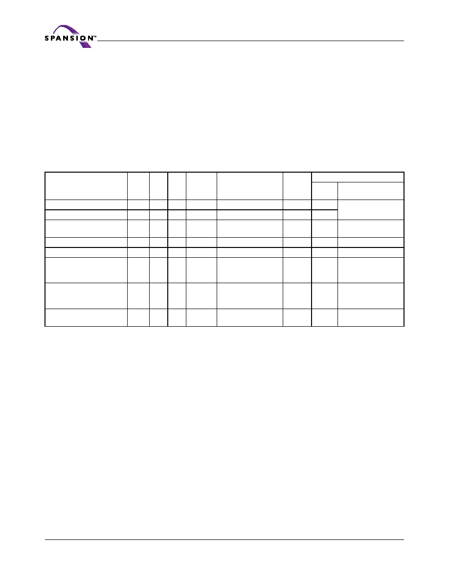
Product Selector Guide
Notes:
1. See
"AC Characteristics"
for full specifications.
2. Contact sales office or representative for availability and ordering information.
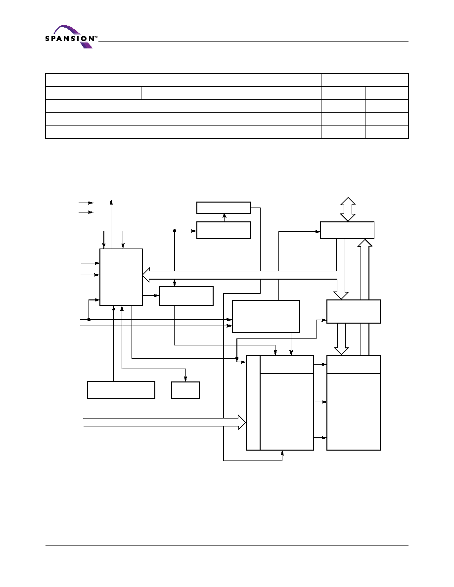
Block Diagram
Family Part Number
S29AL016M
Speed Option
Full Voltage Range: V
CC
= 2.7≠3.6 V
90
100
Max access time (ns)
90
100
Max CE# access time (ns)
90
100
Max OE# access time (ns)
25
25
Input/Output
Buffers
X-Decoder
Y-Decoder
Chip Enable
Output Enable
Logic
Erase Voltage
Generator
PGM Voltage
Generator
Timer
V
CC
Detector
State
Control
Command
Register
V
CC
V
SS
WE#
BYTE#
CE#
OE#
STB
STB
DQ15≠DQ0 (A-1)
Sector Switches
RY/BY#
RESET#
Data
Latch
Y-Gating
Cell Matrix
Ad
d
r
es
s
L
a
tc
h
A19≠A0
April 21, 2004 S29AL016M_00A4
S29AL016M
6
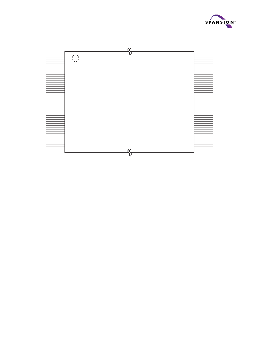
Connection Diagrams
A1
A15
A18
A14
A13
A12
A11
A10
A9
A8
A19
NC
WE#
RESET#
NC
NC
RY/BY#
A17
A7
A6
A5
A4
A3
A2
1
16
2
3
4
5
6
7
8
17
18
19
20
21
22
23
24
9
10
11
12
13
14
15
A16
DQ2
BYTE#
V
SS
DQ15/A-1
DQ7
DQ14
DQ6
DQ13
DQ9
DQ1
DQ8
DQ0
OE#
V
SS
CE#
A0
DQ5
DQ12
DQ4
V
CC
DQ11
DQ3
DQ10
48
33
47
46
45
44
43
42
41
40
39
38
37
36
35
34
25
32
31
30
29
28
27
26
Standard TSOP
7
S29AL016M
S29AL016M_00A4 April 21, 2004
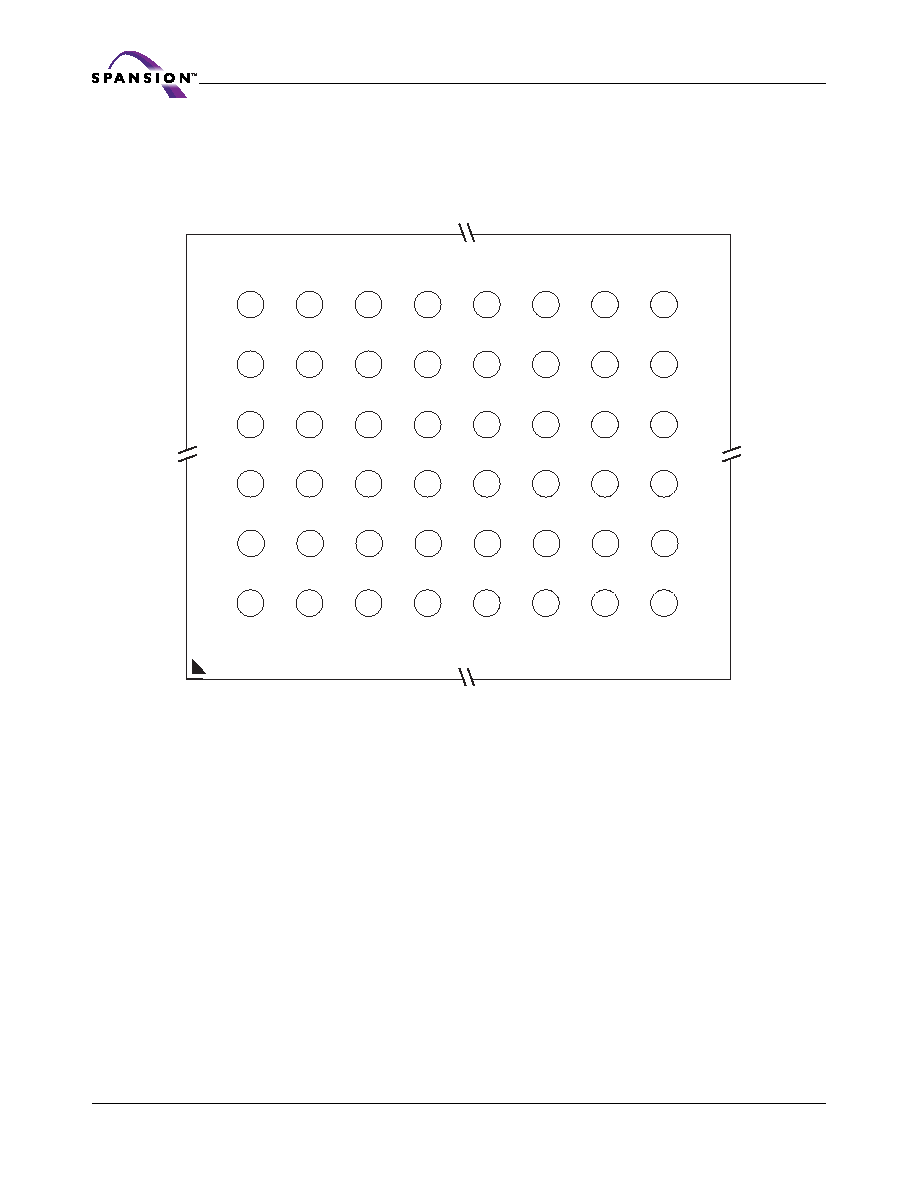
Connection Diagrams
A1
B1
C1
D1
E1
F1
G1
H1
A2
B2
C2
D2
E2
F2
G2
H2
A3
B3
C3
D3
E3
F3
G3
H3
A4
B4
C4
D4
E4
F4
G4
H4
A5
B5
C5
D5
E5
F5
G5
H5
A6
B6
C6
D6
E6
F6
G6
H6
DQ15/A-1
V
SS
BYTE#
A16
A15
A14
A12
A13
DQ13
DQ6
DQ14
DQ7
A11
A10
A8
A9
V
CC
DQ4
DQ12
DQ5
A19
NC
RESET#
WE#
DQ11
DQ3
DQ10
DQ2
NC
A18
NC
RY/BY#
DQ9
DQ1
DQ8
DQ0
A5
A6
A17
A7
OE#
V
SS
CE#
A0
A1
A2
A4
A3
Fine-pitch BGA
Top View, Balls Facing Down
April 21, 2004 S29AL016M_00A4
S29AL016M
8
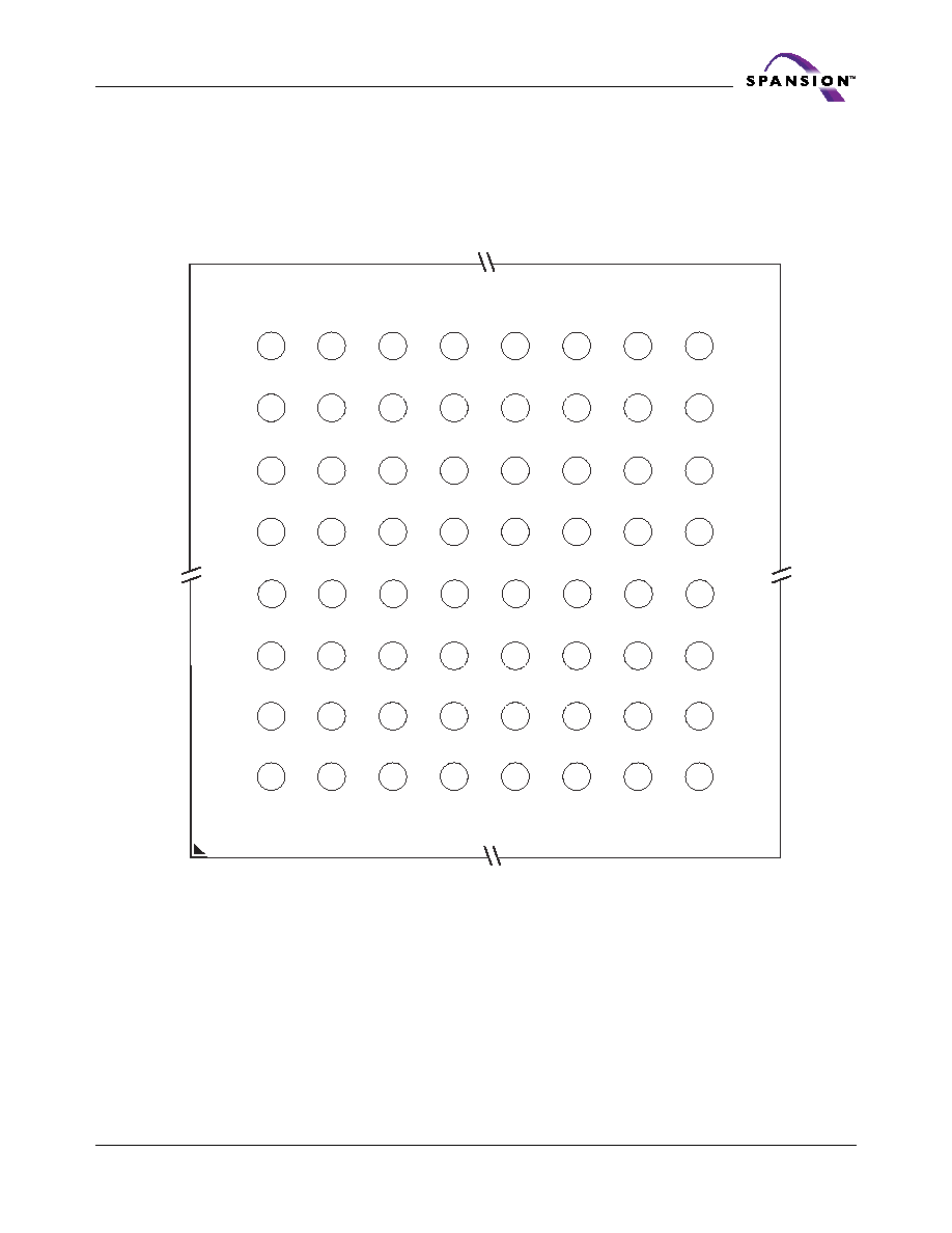
Connection Diagrams
Special Package Handling Instructions
Special handling is required for Flash Memory products in molded packages
(TSOP, BGA, SSOP, PDIP, PLCC). The package and/or data integrity may be
compromised if the package body is exposed to temperatures above 150∞C for
prolonged periods of time.
B3
C3
D3
E3
F3
G3
H3
B4
C4
D4
E4
F4
G4
H4
B5
C5
D5
E5
F5
G5
H5
B6
C6
D6
E6
F6
G6
H6
B7
C7
D7
E7
F7
G7
H7
B8
C8
D8
E8
F8
G8
H8
NC
NC
NC
V
SS
NC
NC
NC
V
SS
DQ15/A-1
BYTE#
A16
A15
A14
A12
DQ6
DQ13
DQ14
DQ7
A11
A10
A8
DQ4
V
CC
DQ12
DQ5
A19
NC
RESET#
DQ3
DQ11
DQ10
DQ2
NC
A18
NC
DQ1
DQ9
DQ8
DQ0
A5
A6
A17
A3
A4
A5
A6
A7
A8
NC
A13
A9
WE#
RY/BY#
A7
B2
C2
D2
E2
F2
G2
H2
V
SS
OE#
CE#
A0
A1
A2
A4
A2
A3
B1
C1
D1
E1
F1
G1
H1
NC
NC
NC
NC
NC
NC
NC
A1
NC
64-Ball Fortified BGA
Top View, Balls Facing Down

9
S29AL016M
S29AL016M_00A4 April 21, 2004
Pin Configuration
A19≠A0
=
20 addresses
DQ14≠DQ0
=
15 data inputs/outputs
DQ15/A-1
=
DQ15 (data input/output, word mode),
A-1 (LSB address input, byte mode)
BYTE#
=
Selects 8-bit or 16-bit mode
CE#
=
Chip enable
OE#
= Output
enable
WE#
=
Write enable
RESET#
=
Hardware reset pin
RY/BY#
= Ready/Busy
output
V
CC
=
3.0 volt-only single power supply
(see Product Selector Guide for speed
options and voltage supply tolerances)
V
SS
=
Device ground
NC
=
Pin not connected internally
Logic Symbol
20
16 or 8
DQ15≠DQ0
(A-1)
A19≠A0
CE#
OE#
WE#
RESET#
BYTE#
RY/BY#

April 21, 2004 S29AL016M_00A4
S29AL016M
10
Ordering Information
Standard Products
Spansion standard products are available in several packages and operating
ranges. The order number (Valid Combination) is formed by a combination of the
elements below.
Valid Combinations
Valid Combinations list configurations planned to be supported in volume for this
device. Consult your local sales office to confirm availability of specific valid com-
binations and to check on newly released combinations.
S29AL016M
90
T
A
I
01
2
PACKING TYPE
0
= Tray
2
= 7" Tape & Reel
3
= 13" Tape & Reel
ADDITIONAL ORDERING OPTIONS
01
= x8/x16, V
CC
= 2.7≠3.6 V, top boot sector device
R1
= x8/x16, V
CC
= 3.0≠3.6 V, top boot sector device
02
= x8/x16, V
CC
= 2.7≠3.6 V, bottom boot sector device
R2
= x8/x16, V
CC
= 3.0≠3.6 V, bottom boot sector device
TEMPERATURE RANGE
I =
Industrial
(≠40
∞
C to +85
∞
C)
PACKAGE MATERIAL SET
A
= Standard
F
= Pb-free
PACKAGE TYPE
T
= Thin Small Outline Package (TSOP) Standard Pinout
B
= Fine-Pitch Ball Grid Array (BGA)
F
= Fortified Ball Grid Array (BGA)
SPEED OPTION
See Product Selector Guide and Valid Combinations
DEVICE NUMBER/DESCRIPTION
S29AL016M
16 Megabit (2M x 8-Bit/1M x 16-Bit) MirrorBit
TM
Flash Memory
3.0 Volt-only Read, Program, and Erase
Note: Characters 1-16 of the OPN represent the TSOP
package marking. For example, the package marking for
OPN S29AL016M90TAI010 is "S29AL016M90TAI01"
Note: Characters 4-16 of the OPN represent the BGA pack-
age marking. For example the package marking for OPN
S29AL016M90BAI010 is "AL016M90BAI01"
Valid Combinations
for TSOP Packages
Package
S29AL016M90
S29AL016M10
TAI
TFI
01
R1
02
R2
TS048
Valid Combinations for BGA Packages
Order Number
Package
S29AL016M90
S29AL016M10
BAI
BFI
01
R1
02
R2
FBA048
FAI
FFI
LAA064
11
S29AL016M
S29AL016M_00A4 April 21, 2004
Device Bus Operations
This section describes the requirements and use of the device bus operations,
which are initiated through the internal command register. The command register
itself does not occupy any addressable memory location. The register is com-
posed of latches that store the commands, along with the address and data
information needed to execute the command. The contents of the register serve
as inputs to the internal state machine. The state machine outputs dictate the
function of the device. Table
1
lists the device bus operations, the inputs and con-
trol levels they require, and the resulting output. The following subsections
describe each of these operations in further detail.
Table 1. S29AL016M Device Bus Operations
Legend: L = Logic Low = V
IL
, H = Logic High = V
IH
, V
ID
= 12.0 ± 0.5 V, X = Don't Care, A
IN
= Address In, D
IN
= Data In, D
OUT
= Data Out
Notes:
1. Addresses are A19:A0 in word mode (BYTE# = V
IH
), A19:A-1 in byte mode (BYTE# = V
IL
).
2. The sector protect and sector unprotect functions may also be implemented via programming equipment. See the "Sector
Protection/Unprotection" section.
Word/Byte Configuration
The BYTE# pin controls whether the device data I/O pins DQ15≠DQ0 operate in
the byte or word configuration. If the BYTE# pin is set at logic `1', the device is in
word configuration, DQ15≠DQ0 are active and controlled by CE# and OE#.
If the BYTE# pin is set at logic `0', the device is in byte configuration, and only
data I/O pins DQ0≠DQ7 are active and controlled by CE# and OE#. The data I/
O pins DQ8≠DQ14 are tri-stated, and the DQ15 pin is used as an input for the
LSB (A-1) address function.
Requirements for Reading Array Data
To read array data from the outputs, the system must drive the CE# and OE# pins
to V
IL
. CE# is the power control and selects the device. OE# is the output control
and gates array data to the output pins. WE# should remain at V
IH
. The BYTE#
pin determines whether the device outputs array data in words or bytes.
Operation
CE# OE# WE# RESET#
Addresses
(Note 1)
DQ0≠
DQ7
DQ8≠DQ15
BYTE#
= V
IH
BYTE#
= V
IL
Read
L
L
H
H
A
IN
D
OUT
D
OUT
DQ8≠DQ14 = High-Z,
DQ15 = A-1
Write
L
H
L
H
A
IN
D
IN
D
IN
Standby
V
CC
±
0.3 V
X
X
V
CC
±
0.3 V
X
High-Z High-Z
High-Z
Output Disable
L
H
H
H
X
High-Z High-Z
High-Z
Reset
X
X
X
L
X
High-Z High-Z
High-Z
Sector Protect (Note 2)
L
H
L
V
ID
Sector Address,
A6 = L, A1 = H,
A0 = L
D
IN
X
X
Sector Unprotect (Note 2)
L
H
L
V
ID
Sector Address,
A6 = H, A1 = H,
A0 = L
D
IN
X
X
Temporary Sector
Unprotect
X
X
X
V
ID
A
IN
D
IN
D
IN
High-Z

April 21, 2004 S29AL016M_00A4
S29AL016M
12
The internal state machine is set for reading array data upon device power-up,
or after a hardware reset. This ensures that no spurious alteration of the mem-
ory content occurs during the power transition. No command is necessary in
this mode to obtain array data. Standard microprocessor read cycles that as-
sert valid addresses on the device address inputs produce valid data on the
device data outputs. The device remains enabled for read access until the com-
mand register contents are altered.
See
"Reading Array Data"
for more information. Refer to the AC
Read Operations
table for timing specifications and to
Figure 13
for the timing diagram. I
CC1
in the
DC Characteristics table represents the active current specification for reading
array data.
Writing Commands/Command Sequences
To write a command or command sequence (which includes programming data
to the device and erasing sectors of memory), the system must drive WE# and
CE# to V
IL
, and OE# to V
IH
.
For program operations, the BYTE# pin determines whether the device accepts
program data in bytes or words. Refer to
"Word Configuration"
for more
information.
The device features an Unlock Bypass mode to facilitate faster programming.
Once the device enters the Unlock Bypass mode, only two write cycles are re-
quired to program a word or byte, instead of four. The
"Word Program Command
Sequence"
section has details on programming data to the device using both
standard and Unlock Bypass command sequences.
An erase operation can erase one sector, multiple sectors, or the entire device.
Tables 2 and 3 indicate the address space that each sector occupies. A "sector
address" consists of the address bits required to uniquely select a sector. The
"Command Definitions"
section has details on erasing a sector or the entire chip,
or suspending/resuming the erase operation.
After the system writes the autoselect command sequence, the device enters the
autoselect mode. The system can then read autoselect codes from the internal
register (which is separate from the memory array) on DQ7≠DQ0. Standard read
cycle timings apply in this mode. Refer to the
"Autoselect Mode"
and
"Autoselect
Command Sequence"
sections for more information.
I
CC2
in the DC Characteristics table represents the active current specification for
the write mode. The
"AC Characteristics"
section contains timing specification ta-
bles and timing diagrams for write operations.
Program and Erase Operation Status
During an erase or program operation, the system may check the status of the
operation by reading the status bits on DQ7≠DQ0. Standard read cycle timings
and I
CC
read specifications apply. Refer to
"Write Operation Status"
for more in-
formation, and to
"AC Characteristics"
for timing diagrams.
Standby Mode
When the system is not reading or writing to the device, it can place the device
in the standby mode. In this mode, current consumption is greatly reduced, and
the outputs are placed in the high impedance state, independent of the OE#
input.

13
S29AL016M
S29AL016M_00A4 April 21, 2004
The device enters the CMOS standby mode when the CE# and RESET# pins are
both held at V
CC
± 0.3 V. (Note that this is a more restricted voltage range than
V
IH
.) If CE# and RESET# are held at V
IH
, but not within V
CC
± 0.3 V, the device
will be in the standby mode, but the standby current will be greater. The device
requires standard access time (t
CE
) for read access when the device is in either
of these standby modes, before it is ready to read data.
If the device is deselected during erasure or programming, the device draws ac-
tive current until the operation is completed.
In the
DC Characteristics
table, I
CC3
and I
CC4
represents the standby current
specification.
Automatic Sleep Mode
The automatic sleep mode minimizes Flash device energy consumption. The
device automatically enables this mode when addresses remain stable for t
ACC
+
30 ns. The automatic sleep mode is independent of the CE#, WE#, and OE#
control signals. Standard address access timings provide new data when
addresses are changed. While in sleep mode, output data is latched and always
available to the system. I
CC4
in the
DC Characteristics
table represents the
automatic sleep mode current specification.
RESET#: Hardware Reset Pin
The RESET# pin provides a hardware method of resetting the device to reading
array data. When the system drives the RESET# pin to V
IL
for at least a period of
t
RP
, the device immediately terminates any operation in progress, tristates all
data output pins, and ignores all read/write attempts for the duration of the RE-
SET# pulse. The device also resets the internal state machine to reading array
data. The operation that was interrupted should be reinitiated once the device is
ready to accept another command sequence, to ensure data integrity.
Current is reduced for the duration of the RESET# pulse. When RESET# is held
at V
SS
±0.3 V, the device draws CMOS standby current (I
CC4
). If RESET# is held
at V
IL
but not within V
SS
±0.3 V, the standby current will be greater.
The RESET# pin may be tied to the system reset circuitry. A system reset would
thus also reset the Flash memory, enabling the system to read the boot-up firm-
ware from the Flash memory.
If RESET# is asserted during a program or erase operation, the RY/BY# pin re-
mains a "0" (busy) until the internal reset operation is complete, which requires
a time of t
READY
(during Embedded Algorithms). The system can thus monitor
RY/BY# to determine whether the reset operation is complete. If RESET# is as-
serted when a program or erase operation is not executing (RY/BY# pin is "1"),
the reset operation is completed within a time of t
READY
(not during Embedded
Algorithms). The system can read data t
RH
after the RESET# pin returns to V
IH
.
Refer to the
AC Characteristics
tables for RESET# parameters and to
Figure 14
for the timing diagram.
Output Disable Mode
When the OE# input is at V
IH
, output from the device is disabled. The output pins
are placed in the high impedance state.
April 21, 2004 S29AL016M_00A4
S29AL016M
14
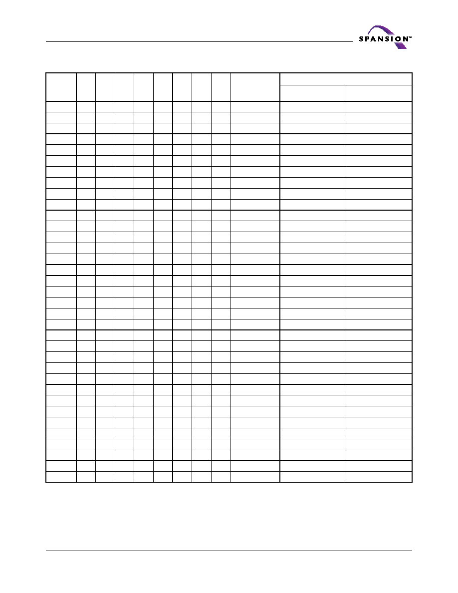
Table 2. Sector Address Tables (Model 01, Top Boot Device)
Note: Address range is A19:A-1 in byte mode and A19:A0 in word mode. See "Word/Byte Configuration" section.
Sector
A19 A18 A17 A16 A15 A14 A13 A12
Sector Size
(Kbytes/
Kwords)
Address Range (in hexadecimal)
Byte Mode (x8)
Word Mode (x16)
SA0
0
0
0
0
0
X
X
X
64/32
000000≠00FFFF
000000≠007FFF
SA1
0
0
0
0
1
X
X
X
64/32
010000≠01FFFF
008000≠00FFFF
SA2
0
0
0
1
0
X
X
X
64/32
020000≠02FFFF
010000≠017FFF
SA3
0
0
0
1
1
X
X
X
64/32
030000≠03FFFF
018000≠01FFFF
SA4
0
0
1
0
0
X
X
X
64/32
040000≠04FFFF
020000≠027FFF
SA5
0
0
1
0
1
X
X
X
64/32
050000≠05FFFF
028000≠02FFFF
SA6
0
0
1
1
0
X
X
X
64/32
060000≠06FFFF
030000≠037FFF
SA7
0
0
1
1
1
X
X
X
64/32
070000≠07FFFF
038000≠03FFFF
SA8
0
1
0
0
0
X
X
X
64/32
080000≠08FFFF
040000≠047FFF
SA9
0
1
0
0
1
X
X
X
64/32
090000≠09FFFF
048000≠04FFFF
SA10
0
1
0
1
0
X
X
X
64/32
0A0000≠0AFFFF
050000≠057FFF
SA11
0
1
0
1
1
X
X
X
64/32
0B0000≠0BFFFF
058000≠05FFFF
SA12
0
1
1
0
0
X
X
X
64/32
0C0000≠0CFFFF
060000≠067FFF
SA13
0
1
1
0
1
X
X
X
64/32
0D0000≠0DFFFF
068000≠06FFFF
SA14
0
1
1
1
0
X
X
X
64/32
0E0000≠0EFFFF
070000≠077FFF
SA15
0
1
1
1
1
X
X
X
64/32
0F0000≠0FFFFF
078000≠07FFFF
SA16
1
0
0
0
0
X
X
X
64/32
100000≠10FFFF
080000≠087FFF
SA17
1
0
0
0
1
X
X
X
64/32
110000≠11FFFF
088000≠08FFFF
SA18
1
0
0
1
0
X
X
X
64/32
120000≠12FFFF
090000≠097FFF
SA19
1
0
0
1
1
X
X
X
64/32
130000≠13FFFF
098000≠09FFFF
SA20
1
0
1
0
0
X
X
X
64/32
140000≠14FFFF
0A0000≠0A7FFF
SA21
1
0
1
0
1
X
X
X
64/32
150000≠15FFFF
0A8000≠AFFFF
SA22
1
0
1
1
0
X
X
X
64/32
160000≠16FFFF
0B0000≠0B7FFF
SA23
1
0
1
1
1
X
X
X
64/32
170000≠17FFFF
0B8000≠0BFFFF
SA24
1
1
0
0
0
X
X
X
64/32
180000≠18FFFF
0C0000≠0C7FFF
SA25
1
1
0
0
1
X
X
X
64/32
190000≠19FFFF
0C8000≠0CFFFF
SA26
1
1
0
1
0
X
X
X
64/32
1A0000≠1AFFFF
0D0000≠0D7FFF
SA27
1
1
0
1
1
X
X
X
64/32
1B0000≠1BFFFF
0D8000≠0DFFFF
SA28
1
1
1
0
0
X
X
X
64/32
1C0000≠1CFFFF
0E0000≠0E7FFF
SA29
1
1
1
0
1
X
X
X
64/32
1D0000≠1DFFFF
0E8000≠0EFFFF
SA30
1
1
1
1
0
X
X
X
64/32
1E0000≠1EFFFF
0F0000≠0F7FFF
SA31
1
1
1
1
1
0
X
X
32/16
1F0000≠1F7FFF
0F8000≠0FBFFF
SA32
1
1
1
1
1
1
0
0
8/4
1F8000≠1F9FFF
0FC000≠0FCFFF
SA33
1
1
1
1
1
1
0
1
8/4
1FA000≠1FBFFF
0FD000≠0FDFFF
SA34
1
1
1
1
1
1
1
X
16/8
1FC000≠1FFFFF
0FE000≠0FFFFF
15
S29AL016M
S29AL016M_00A4 April 21, 2004
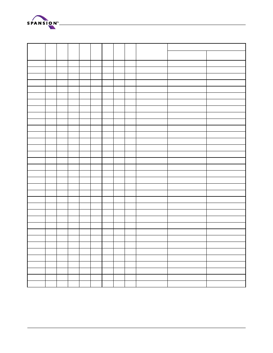
Table 3. Sector Address Tables (Model 02, Bottom Boot Device)
Note: Address range is A19:A-1 in byte mode and A19:A0 in word mode. See the "Word/Byte Configuration" section.
Autoselect Mode
The autoselect mode provides manufacturer and device identification, and sector
protection verification, through identifier codes output on DQ7≠DQ0. This mode
is primarily intended for programming equipment to automatically match a device
Sector A19 A18 A17 A16 A15 A14 A13 A12
Sector Size
(Kbytes/
Kwords)
Address Range (in hexadecimal)
Byte Mode (x8)
Word Mode (x16)
SA0
0
0
0
0
0
0
0
X
16/8
000000≠003FFF
000000≠001FFF
SA1
0
0
0
0
0
0
1
0
8/4
004000≠005FFF
002000≠002FFF
SA2
0
0
0
0
0
0
1
1
8/4
006000≠007FFF
003000≠003FFF
SA3
0
0
0
0
0
1
X
X
32/16
008000≠00FFFF
004000≠007FFF
SA4
0
0
0
0
1
X
X
X
64/32
010000≠01FFFF
008000≠00FFFF
SA5
0
0
0
1
0
X
X
X
64/32
020000≠02FFFF
010000≠017FFF
SA6
0
0
0
1
1
X
X
X
64/32
030000≠03FFFF
018000≠01FFFF
SA7
0
0
1
0
0
X
X
X
64/32
040000≠04FFFF
020000≠027FFF
SA8
0
0
1
0
1
X
X
X
64/32
050000≠05FFFF
028000≠02FFFF
SA9
0
0
1
1
0
X
X
X
64/32
060000≠06FFFF
030000≠037FFF
SA10
0
0
1
1
1
X
X
X
64/32
070000≠07FFFF
038000≠03FFFF
SA11
0
1
0
0
0
X
X
X
64/32
080000≠08FFFF
040000≠047FFF
SA12
0
1
0
0
1
X
X
X
64/32
090000≠09FFFF
048000≠04FFFF
SA13
0
1
0
1
0
X
X
X
64/32
0A0000≠0AFFFF
050000≠057FFF
SA14
0
1
0
1
1
X
X
X
64/32
0B0000≠0BFFFF
058000≠05FFFF
SA15
0
1
1
0
0
X
X
X
64/32
0C0000≠0CFFFF
060000≠067FFF
SA16
0
1
1
0
1
X
X
X
64/32
0D0000≠0DFFFF
068000≠06FFFF
SA17
0
1
1
1
0
X
X
X
64/32
0E0000≠0EFFFF
070000≠077FFF
SA18
0
1
1
1
1
X
X
X
64/32
0F0000≠0FFFFF
078000≠07FFFF
SA19
1
0
0
0
0
X
X
X
64/32
100000≠10FFFF
080000≠087FFF
SA20
1
0
0
0
1
X
X
X
64/32
110000≠11FFFF
088000≠08FFFF
SA21
1
0
0
1
0
X
X
X
64/32
120000≠12FFFF
090000≠097FFF
SA22
1
0
0
1
1
X
X
X
64/32
130000≠13FFFF
098000≠09FFFF
SA23
1
0
1
0
0
X
X
X
64/32
140000≠14FFFF
0A0000≠0A7FFF
SA24
1
0
1
0
1
X
X
X
64/32
150000≠15FFFF
0A8000≠0AFFFF
SA25
1
0
1
1
0
X
X
X
64/32
160000≠16FFFF
0B0000≠0B7FFF
SA26
1
0
1
1
1
X
X
X
64/32
170000≠17FFFF
0B8000≠0BFFFF
SA27
1
1
0
0
0
X
X
X
64/32
180000≠18FFFF
0C0000≠0C7FFF
SA28
1
1
0
0
1
X
X
X
64/32
190000≠19FFFF
0C8000≠0CFFFF
SA29
1
1
0
1
0
X
X
X
64/32
1A0000≠1AFFFF
0D0000≠0D7FFF
SA30
1
1
0
1
1
X
X
X
64/32
1B0000≠1BFFFF
0D8000≠0DFFFF
SA31
1
1
1
0
0
X
X
X
64/32
1C0000≠1CFFFF
0E0000≠0E7FFF
SA32
1
1
1
0
1
X
X
X
64/32
1D0000≠1DFFFF
0E8000≠0EFFFF
SA33
1
1
1
1
0
X
X
X
64/32
1E0000≠1EFFFF
0F0000≠0F7FFF
SA34
1
1
1
1
1
X
X
X
64/32
1F0000≠1FFFFF
0F8000≠0FFFFF
April 21, 2004 S29AL016M_00A4
S29AL016M
16
to be programmed with its corresponding programming algorithm. However, the
autoselect codes can also be accessed in-system through the command register.
When using programming equipment, the autoselect mode requires V
ID
(11.5 V
to 12.5 V) on address pin A9. Address pins A6, A1, and A0 must be as shown in
Table
4
. In addition, when verifying sector protection, the sector address must
appear on the appropriate highest order address bits (see Tables
2
and
3
). Table
4
shows the remaining address bits that are don't care. When all necessary bits
have been set as required, the programming equipment may then read the cor-
responding identifier code on DQ7-DQ0.
To access the autoselect codes in-system, the host system can issue the autose-
lect command via the command register, as shown in Tables
10
≠
11
. This method
does not require V
ID
. See
"Command Definitions"
for details on using the autose-
lect mode.
Table 4. Autoselect Codes (High Voltage Method)
L = Logic Low = V
IL
, H = Logic High = V
IH
, SA = Sector Address, X = Don't care.
Note: The autoselect codes may also be accessed in-system via command sequences. See Tables
10
≠
11
.
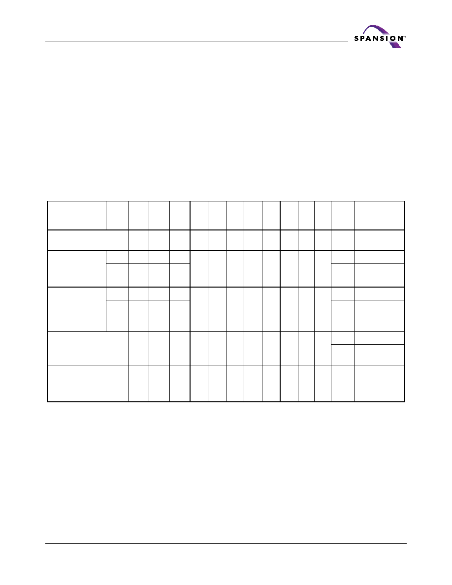
Sector Protection/Unprotection
The hardware sector protection feature disables both program and erase opera-
tions in any sector. The hardware sector unprotection feature re-enables both
program and erase operations in previously protected sectors.
The device is normally shipped with all sectors unprotected. However, the Ex-
pressFlashTM Service offers the option of programming and protecting sectors at
the factory prior to shipping the device. Contact a sales office or representative
for details.
It is possible to determine whether a sector is protected or unprotected. See
"Au-
toselect Mode"
for details.
Description
Mode CE# OE# WE#
A19
to
A12
A11
to
A10 A9
A8
to
A7
A6
A5
to
A2
A1
A0
DQ8
to
DQ15
DQ7
to
DQ0
Manufacturer ID
(Spansion Products)
L
L
H
X
X
V
ID
X
L
X
L
L
X
01h
Device ID:
S29AL016M
(Model 01)
(Top Boot Block)
Word
L
L
H
X
X
V
ID
X
L
X
L
H
22h
C4h
Byte
L
L
H
X
C4h
Device ID:
S29AL016M
(Model 02)
(Bottom Boot
Block)
Word
L
L
H
X
X
V
ID
X
L
X
L
H
22h
49h
Byte
L
L
H
X
49h
Sector Protection
Verification
L
L
H
SA
X
V
ID
X
L
X
H
L
X
01h (protected)
X
00h
(unprotected)
SecSi Sector Indicator Bit
(DQ7)
L
L
H
X
X
V
ID
X
H
X
L
H
X
83 (factory
locked
03h (not
factory locked)
17
S29AL016M
S29AL016M_00A4 April 21, 2004
Sector protection and unprotection requires V
ID
on the RESET# pin only, and can
be implemented either in-system or via programming equipment.
Figure 2
shows
the algorithms and
Figure 23
shows the timing diagram. This method uses stan-
dard microprocessor bus cycle timing. For sector unprotect, all unprotected
sectors must first be protected prior to the first sector unprotect write cycle.
Temporary Sector Unprotect
This feature allows temporary unprotection of previously protected sectors to
change data in-system. The Sector Unprotect mode is activated by setting the
RESET# pin to V
ID
. During this mode, formerly protected sectors can be pro-
grammed or erased by selecting the sector addresses. Once V
ID
is removed from
the RESET# pin, all the previously protected sectors are protected again.
Figure
shows the algorithm, and
Figure 22
shows the timing diagrams, for this feature.
Notes:
1. All protected sectors unprotected.
2. All previously protected sectors are protected once again.
Figure 1. Temporary Sector Unprotect Operation
START
Perform Erase or
Program Operations
RESET# = V
IH
Temporary Sector
Unprotect Completed
(Note 2)
RESET# = V
ID
(Note 1)
April 21, 2004 S29AL016M_00A4
S29AL016M
18
Figure 2. In-System Single High Voltage Sector Protect/Unprotect Algorithms
Sector Protect:
Write 60h to sector
address with
A6 = 0, A1 = 1,
A0 = 0
Set up sector
address
Wait 150 µs
Verify Sector
Protect: Write 40h
to sector address
with A6 = 0,
A1 = 1, A0 = 0
Read from
sector address
with A6 = 0,
A1 = 1, A0 = 0
START
PLSCNT = 1
RESET# = V
ID
Wait 1 ms
First Write
Cycle = 60h?
Data = 01h?
Remove V
ID
from RESET#
Write reset
command
Sector Protect
complete
Yes
Yes
No
PLSCNT
= 25?
Yes
Device failed
Increment
PLSCNT
Temporary Sector
Unprotect Mode
No
Sector Unprotect:
Write 60h to sector
address with
A6 = 1, A1 = 1,
A0 = 0
Set up first sector
address
Wait 15 ms
Verify Sector
Unprotect: Write
40h to sector
address with
A6 = 1, A1 = 1,
A0 = 0
Read from
sector address
with A6 = 1,
A1 = 1, A0 = 0
START
PLSCNT = 1
RESET# = V
ID
Wait 1 ms
Data = 00h?
Last sector
verified?
Remove V
ID
from RESET#
Write reset
command
Sector Unprotect
complete
Yes
No
PLSCNT
= 1000?
Yes
Device failed
Increment
PLSCNT
Temporary Sector
Unprotect Mode
No
All sectors
protected?
Yes
Protect all sectors:
The indicated portion
of the sector protect
algorithm must be
performed for all
unprotected sectors
prior to issuing the
first sector
unprotect address
Set up
next sector
address
No
Yes
No
Yes
No
No
Yes
No
In-System Single
High Voltage
Sector Protect
Algorithm
In-System Single
High Voltage
Sector Unprotect
Algorithm
First Write
Cycle = 60h?
Protect another
sector?
Reset
PLSCNT = 1

19
S29AL016M
S29AL016M_00A4 April 21, 2004
SecSi (Secured Silicon) Sector Flash Memory Region
The SecSi (Secured Silicon) Sector feature provides a Flash memory region that
enables permanent part identification through an Electronic Serial Number
(ESN). The SecSi Sector is 256 bytes in length, and uses a SecSi Sector Indica-
tor Bit (DQ7) to indicate whether or not the SecSi Sector is locked when shipped
from the factory. This bit is permanently set at the factory and cannot be
changed, which prevents cloning of a factory locked part. This ensures the secu-
rity of the ESN once the product is shipped to the field.
The device is offered with the SecSi Sector either customer lockable (standard
shipping option) or factory locked (contact a sales office or representative for or-
dering information). The customer-lockable version is shipped with the SecSi
Sector unprotected, allowing customers to program the sector after receiving
the device. The customer-lockable version also has the SecSi Sector Indicator
Bit permanently set to a "0." The factory-locked version is always protected
when shipped from the factory, and has the SecSi (Secured Silicon) Sector Indi-
cator Bit permanently set to a "1." Thus, the SecSi Sector Indicator Bit prevents
customer-lockable devices from being used to replace devices that are factory
locked. Note that the ACC function and unlock bypass modes are not available
when the SecSi Sector is enabled.
The SecSi sector address space in this device is allocated as follows:
Table 5. SecSi Sector Addressing
The system accesses the SecSi Sector through a command sequence (see "En-
ter SecSi Sector/Exit SecSi Sector Command Sequence"). After the system has
written the Enter SecSi Sector command sequence, it may read the SecSi Sector
by using the addresses normally occupied by the first sector (SA0). This mode of
operation continues until the system issues the Exit SecSi Sector command se-
quence, or until power is removed from the device. On power-up, or following a
hardware reset, the device reverts to sending commands to sector SA0.
Customer Lockable: SecSi Sector NOT Programmed or Protected
At the Factory
Unless otherwise specified, the device is shipped such that the customer may
program and protect the 256-byte SecSi sector.
The system may program the SecSi Sector using the write-buffer, accelerated
and/or unlock bypass methods, in addition to the standard programming com-
mand sequence. See Command Definitions.
Programming and protecting the SecSi Sector must be used with caution since,
once protected, there is no procedure available for unprotecting the SecSi Sec-
tor area and none of the bits in the SecSi Sector memory space can be modified
in any way.
The SecSi Sector area can be protected using one of the following procedures:
Write the three-cycle Enter SecSi Sector Region command sequence, and
then follow the in-system sector protect algorithm as shown in Figure 2, ex-
SecSi Sector Address Range
Customer
Lockable
ESN Factory
Locked
ExpressFlash
Factory Locked
x16
x8
0F8000h≠
0F8007h
0F8000h≠
0F800Fh
Determined by
customer
ESN
ESN or determined
by customer
0F8008h≠
0F807Fh
0F8010h≠
0F80FFh
Unavailable
Determined
by customer
April 21, 2004 S29AL016M_00A4
S29AL016M
20
cept that RESET# may be at either V
IH
or V
ID
. This allows in-system protec-
tion of the SecSi Sector without raising any device pin to a high voltage. Note
that this method is only applicable to the SecSi Sector.
To verify the protect/unprotect status of the SecSi Sector, follow the algo-
rithm shown in Figure 3.
Once the SecSi Sector is programmed, locked and verified, the system must
write the Exit SecSi Sector Region command sequence to return to reading and
writing within the remainder of the array.
Factory Locked: SecSi Sector Programmed and Protected At the
Factory
In devices with an ESN, the SecSi Sector is protected when the device is shipped
from the factory. The SecSi Sector cannot be modified in any way. An ESN Fac-
tory Locked device has a 16-byte random ESN at addresses 0F8000h≠0F8007h.
Please contact your local sales office or representative for details on ordering ESN
Factory Locked devices.
Customers may opt to have their code programmed by the manufacturer
through the ExpressFlash service (Express Flash Factory Locked). The devices
are then shipped from the factory with the SecSi Sector permanently locked.
Contact an sales office or representative for details on using the ExpressFlash
service.
Figure 3. SecSi Sector Protect Verify
Common Flash Memory Interface (CFI)
The Common Flash Interface (CFI) specification outlines device and host system
software interrogation handshake, which allows specific vendor-specified soft-
ware algorithms to be used for entire families of devices. Software support can
then be device-independent, JEDEC ID-independent, and forward- and back-
Write 60h to
any address
Write 40h to SecSi
Sector address
with A6 = 0,
A1 = 1, A0 = 0
START
RESET# =
V
IH
or V
ID
Wait 1 ms
Read from SecSi
Sector address
with A6 = 0,
A1 = 1, A0 = 0
If data = 00h,
SecSi Sector is
unprotected.
If data = 01h,
SecSi Sector is
protected.
Remove V
IH
or V
ID
from RESET#
Write reset
command
SecSi Sector
Protect Verify
complete
21
S29AL016M
S29AL016M_00A4 April 21, 2004
ward-compatible for the specified flash device families. Flash vendors can
standardize their existing interfaces for long-term compatibility.
This device enters the CFI Query mode when the system writes the CFI Query
command, 98h, to address 55h in word mode (or address AAh in byte mode), any
time the device is ready to read array data. The system can read CFI information
at the addresses given in Tables
6
≠
9
. In word mode, the upper address bits (A7≠
MSB) must be all zeros. To terminate reading CFI data, the system must write
the reset command.
The system can also write the CFI query command when the device is in the au-
toselect mode. The device enters the CFI query mode, and the system can read
CFI data at the addresses given in Tables
6
≠
9
. The system must write the reset
command to return the device to the read/reset mode.
For further information, please refer to the CFI Specification and CFI Publication
100, available online at
http://www.amd.com/flash/cfi
. Alternatively, contact an
sales office or representative for copies of these documents.
Table 6. CFI Query Identification String
Addresses
(Word Mode)
Addresses
(Byte Mode)
Data
Description
10h
11h
12h
20h
22h
24h
0051h
0052h
0059h
Query Unique ASCII string "QRY"
13h
14h
26h
28h
0002h
0000h
Primary OEM Command Set
15h
16h
2Ah
2Ch
0040h
0000h
Address for Primary Extended Table
17h
18h
2Eh
30h
0000h
0000h
Alternate OEM Command Set (00h = none exists)
19h
1Ah
32h
34h
0000h
0000h
Address for Alternate OEM Extended Table (00h = none exists)
April 21, 2004 S29AL016M_00A4
S29AL016M
22
Note: CFI data related to timeouts may differ from actual timeouts of the product. Consult the Ordering the Erase and
Programming Performance table for timeout guidelines.
Table 7. System Interface String
Addresses
(Word Mode)
Addresses
(Byte Mode)
Data
Description
1Bh
36h
0027h
V
CC
Min. (write/erase). D7≠D4: volt, D3≠D0: 100 millivolt
1Ch
38h
0036h
V
CC
Max. (write/erase). D7≠D4: volt, D3≠D0: 100 millivolt
1Dh
3Ah
0000h
V
PP
Min. voltage (00h = no V
PP
pin present)
1Eh
3Ch
0000h
V
PP
Max. voltage (00h = no V
PP
pin present)
1Fh
3Eh
0007h
Typical timeout per single byte/word write 2
N
µs
20h
40h
0000h
Typical timeout for Min. size buffer write 2
N
µs (00h = not supported)
21h
42h
000Ah
Typical timeout per individual block erase 2
N
ms
22h
44h
0000h
Typical timeout for full chip erase 2
N
ms (00h = not supported)
23h
46h
0001h
Reserved for future use
24h
48h
0000h
Max. timeout for buffer write 2
N
times typical (00h = not supported)
25h
4Ah
0004h
Max. timeout per individual block erase 2
N
times typical
26h
4Ch
0000h
Max. timeout for full chip erase 2
N
times typical (00h = not supported)
Table 8. Device Geometry Definition
Addresses
(Word Mode)
Addresses
(Byte Mode)
Data
Description
27h
4Eh
0015h
Device Size = 2
N
byte
28h
29h
50h
52h
0002h
0000h
Flash Device Interface description (refer to CFI publication 100)
2Ah
2Bh
54h
56h
0000h
0000h
Max. number of byte in multi-byte write = 2
N
(00h = not supported)
2Ch
58h
0004h
Number of Erase Block Regions within device
2Dh
2Eh
2Fh
30h
5Ah
5Ch
5Eh
60h
0000h
0000h
0040h
0000h
Erase Block Region 1 Information
(refer to the CFI specification or CFI publication 100)
31h
32h
33h
34h
62h
64h
66h
68h
0001h
0000h
0020h
0000h
Erase Block Region 2 Information
35h
36h
37h
38h
6Ah
6Ch
6Eh
70h
0000h
0000h
0080h
0000h
Erase Block Region 3 Information
39h
3Ah
3Bh
3Ch
72h
74h
76h
78h
001Eh
0000h
0000h
0001h
Erase Block Region 4 Information

23
S29AL016M
S29AL016M_00A4 April 21, 2004
Hardware Data Protection
The command sequence requirement of unlock cycles for programming or erasing
provides data protection against inadvertent writes (refer to Tables
10
≠
11
for
command definitions). In addition, the following hardware data protection mea-
sures prevent accidental erasure or programming, which might otherwise be
caused by spurious system level signals during V
CC
power-up and power-down
transitions, or from system noise.
Low V
CC
Write Inhibit
When V
CC
is less than V
LKO
, the device does not accept any write cycles. This pro-
tects data during V
CC
power-up and power-down. The command register and all
internal program/erase circuits are disabled, and the device resets. Subsequent
writes are ignored until V
CC
is greater than V
LKO
. The system must provide the
proper signals to the control pins to prevent unintentional writes when V
CC
is
greater than V
LKO
.
Write Pulse "Glitch" Protection
Noise pulses of less than 5 ns (typical) on OE#, CE# or WE# do not initiate a write
cycle.
Table 9. Primary Vendor-Specific Extended Query
Addresses
(Word Mode)
Addresses
(Byte Mode)
Data
Description
40h
41h
42h
80h
82h
84h
0050h
0052h
0049h
Query-unique ASCII string "PRI"
43h
86h
0031h
Major version number, ASCII
44h
88h
0033h
Minor version number, ASCII
45h
8Ah
0008h
Address Sensitive Unlock (Bit 1≠0)
0b = Required, 1b = Not Required
Process Technology (Bits 7≠2)
0010b = 0.23 µm MirrorBit
46h
8Ch
0002h
Erase Suspend
0 = Not Supported, 1 = To Read Only, 2 = To Read & Write
47h
8Eh
0001h
Sector Protect
0 = Not Supported, X = Number of sectors in per group
48h
90h
0001h
Sector Temporary Unprotect
00 = Not Supported, 01 = Supported
49h
92h
0004h
Sector Protect/Unprotect scheme
04 = Standard Mode
4Ah
94h
0000h
Simultaneous Operation
00 = Not Supported, 01 = Supported
4Bh
96h
0000h
Burst Mode Type
00 = Not Supported, 01 = Supported
4Ch
98h
0000h
Page Mode Type
00 = Not Supported, 01 = 4 Word Page, 02 = 8 Word Page

April 21, 2004 S29AL016M_00A4
S29AL016M
24
Logical Inhibit
Write cycles are inhibited by holding any one of OE# = V
IL
, CE# = V
IH
or WE# =
V
IH
. To initiate a write cycle, CE# and WE# must be a logical zero while OE# is a
logical one.
Power-Up Write Inhibit
If WE# = CE# = V
IL
and OE# = V
IH
during power up, the device does not accept
commands on the rising edge of WE#. The internal state machine is automatically
reset to reading array data on power-up.
Command Definitions
Writing specific address and data commands or sequences into the command
register initiates device operations. Tables
10
≠
11
define the valid register com-
mand sequences. Note that writing incorrect address and data values or writing
them in the improper sequence may place the device in an unknown state. A
reset command is then required to set the device for the next operation.
All addresses are latched on the falling edge of WE# or CE#, whichever happens
later. All data is latched on the rising edge of WE# or CE#, whichever happens
first. Refer to the appropriate timing diagrams in the
"AC Characteristics"
section.
Reading Array Data
The device is automatically set to reading array data after device power-up. No
commands are required to retrieve data. The device is also ready to read array
data after completing an Embedded Program or Embedded Erase algorithm.
After the device accepts an Erase Suspend command, the device enters the
Erase Suspend mode. The system can read array data using the standard read
timings, except that if it reads at an address within erase-suspended sectors,
the device outputs status data. After completing a programming operation in
the Erase Suspend mode, the system may once again read array data with the
same exception. See
"Erase Suspend/Erase Resume Commands"
for more in-
formation on this mode.
The system must issue the reset command to re-enable the device for reading
array data if DQ5 goes high, or while in the autoselect mode. See the
"Reset Com-
mand"
section, next.
See also
"Requirements for Reading Array Data"
in the
"Device Bus Operations"
section for more information. The
Read Operations
table provides the read pa-
rameters, and
Figure 13
shows the timing diagram.
Reset Command
Writing the reset command to the device resets the device to reading array data.
Address bits are don't care for this command.
The reset command may be written between the sequence cycles in an erase
command sequence before erasing begins. This resets the device to reading array
data. Once erasure begins, however, the device ignores reset commands until the
operation is complete.
The reset command may be written between the sequence cycles in a program
command sequence before programming begins. This resets the device to read-
ing array data (also applies to programming in Erase Suspend mode). Once
programming begins, however, the device ignores reset commands until the op-
eration is complete.

25
S29AL016M
S29AL016M_00A4 April 21, 2004
The reset command may be written between the sequence cycles in an autoselect
command sequence. Once in the autoselect mode, the reset command must be
written to return to reading array data (also applies to autoselect during Erase
Suspend).
If DQ5 goes high during a program or erase operation, writing the reset command
returns the device to reading array data (also applies during Erase Suspend).
Autoselect Command Sequence
The autoselect command sequence allows the host system to access the manu-
facturer and devices codes, and determine whether or not a sector is protected.
Tables
10
≠
11
show the address and data requirements. This method is an alter-
native to that shown in Table
4
, which is intended for PROM programmers and
requires V
ID
on address bit A9.
The autoselect command sequence is initiated by writing two unlock cycles, fol-
lowed by the autoselect command. The device then enters the autoselect mode,
and the system may read at any address any number of times, without initiating
another command sequence.
A read cycle at address XX00h retrieves the manufacturer code. A read cycle at
address XX01h returns the device code. A read cycle containing a sector address
(SA) and the address XX02h in word mode (or XX04h in byte mode) returns
XX01h if that sector is protected, or 00h if it is unprotected. Refer to Tables
2
and
3
for valid sector addresses.
The system must write the reset command to exit the autoselect mode and return
to reading array data.
Word/Byte Program Command Sequence
The system may program the device by word or byte, depending on the state
of the BYTE# pin. Programming is a four-bus-cycle operation. The program
command sequence is initiated by writing two unlock write cycles, followed by
the program set-up command. The program address and data are written next,
which in turn initiate the Embedded Program algorithm. The system is not re-
quired to provide further controls or timings. The device automatically
generates the program pulses and verifies the programmed cell margin. Tables
10
≠
11
show the address and data requirements for the program command se-
quence. Note that the SecSi Sector, autoselect, and CFI functions are
unavailable when a program operation is in progress.
When the Embedded Program algorithm is complete, the device then returns to
reading array data and addresses are no longer latched. The system can deter-
mine the status of the program operation by using DQ7, DQ6, or RY/BY#. See
"Write Operation Status"
for information on these status bits.
Any commands written to the device during the Embedded Program Algorithm
are ignored. Note that a hardware reset immediately terminates the program-
ming operation. The Program command sequence should be reinitiated once the
device has reset to reading array data, to ensure data integrity.
Programming is allowed in any sequence and across sector boundaries. Program-
ming to the same address multiple times without intervening erases is limited.
For such application requirements, please contact your local Spansion represen-
tative. Any bit in a word or byte cannot be programmed from "0" back to a
"1". Attempting to do so may halt the operation and set DQ5 to "1," or cause the
Data# Polling algorithm to indicate the operation was successful. However, a suc-

April 21, 2004 S29AL016M_00A4
S29AL016M
26
ceeding read will show that the data is still "0". Only erase operations can convert
a "0" to a "1".
Unlock Bypass Command Sequence
The unlock bypass feature allows the system to program bytes or words to the
device faster than using the standard program command sequence. The unlock
bypass command sequence is initiated by first writing two unlock cycles. This is
followed by a third write cycle containing the unlock bypass command, 20h. The
device then enters the unlock bypass mode. A two-cycle unlock bypass program
command sequence is all that is required to program in this mode. The first cycle
in this sequence contains the unlock bypass program command, A0h; the second
cycle contains the program address and data. Additional data is programmed in
the same manner. This mode dispenses with the initial two unlock cycles required
in the standard program command sequence, resulting in faster total program-
ming time. Tables
10
≠
11
show the requirements for the command sequence.
During the unlock bypass mode, only the Unlock Bypass Program and Unlock By-
pass Reset commands are valid. To exit the unlock bypass mode, the system
must issue the two-cycle unlock bypass reset command sequence. The first cycle
must contain the data 90h; the second cycle the data 00h. Addresses are don't
care for both cycles. The device then returns to reading array data.
Figure 4
illustrates the algorithm for the program operation. See the
Erase/Pro-
gram Operations
table in
"AC Characteristics"
for parameters, and to
Figure 17
for timing diagrams.
27
S29AL016M
S29AL016M_00A4 April 21, 2004
Notes: See Tables 10 and 11 for program command sequence.
Figure 4. Program Operation
Chip Erase Command Sequence
Chip erase is a six bus cycle operation. The chip erase command sequence is ini-
tiated by writing two unlock cycles, followed by a set-up command. Two
additional unlock write cycles are then followed by the chip erase command,
which in turn invokes the Embedded Erase algorithm. The device does not require
the system to preprogram prior to erase. The Embedded Erase algorithm auto-
matically preprograms and verifies the entire memory for an all zero data pattern
prior to electrical erase. The system is not required to provide any controls or tim-
ings during these operations. Tables
10
≠
11
show the address and data
requirements for the chip erase command sequence. Note that the SecSi Sector,
autoselect, and CFI functions are unavailable when an erase operation is in
progress.
Any commands written to the chip during the Embedded Erase algorithm are ig-
nored. Note that a hardware reset during the chip erase operation immediately
terminates the operation. The Chip Erase command sequence should be reiniti-
ated once the device has returned to reading array data, to ensure data integrity.
The system can determine the status of the erase operation by using DQ7, DQ6,
DQ2, or RY/BY#. See
"Autoselect Command Sequence"
for information on these
status bits. When the Embedded Erase algorithm is complete, the device returns
to reading array data and addresses are no longer latched.
START
Write Program
Command Sequence
Data Poll
from System
Verify Data?
No
Yes
Last Address?
No
Yes
Programming
Completed
Increment Address
Embedded
Program
algorithm
in progress

April 21, 2004 S29AL016M_00A4
S29AL016M
28
Figure 5
illustrates the algorithm for the erase operation. See the
Erase/Program
Operations
tables in
"AC Characteristics"
for parameters, and to
Figure 18
for tim-
ing diagrams.
Sector Erase Command Sequence
Sector erase is a six bus cycle operation. The sector erase command sequence is
initiated by writing two unlock cycles, followed by a set-up command. Two addi-
tional unlock write cycles are then followed by the address of the sector to be
erased, and the sector erase command. Tables
10
≠
11
show the address and data
requirements for the sector erase command sequence. Note that the SecSi Sec-
tor, autoselect, and CFI functions are unavailable when an erase operation is
in progress.
The device does not require the system to preprogram the memory prior to erase.
The Embedded Erase algorithm automatically programs and verifies the sector for
an all zero data pattern prior to electrical erase. The system is not required to
provide any controls or timings during these operations.
After the command sequence is written, a sector erase time-out of 50 µs begins.
During the time-out period, additional sector addresses and sector erase com-
mands may be written. Loading the sector erase buffer may be done in any
sequence, and the number of sectors may be from one sector to all sectors. The
time between these additional cycles must be less than 50 µs, otherwise the last
address and command might not be accepted, and erasure may begin. It is rec-
ommended that processor interrupts be disabled during this time to ensure all
commands are accepted. The interrupts can be re-enabled after the last Sector
Erase command is written. If the time between additional sector erase commands
can be assumed to be less than 50 µs, the system need not monitor DQ3. Any
command other than Sector Erase or Erase Suspend during the time-out
period resets the device to reading array data. The system must rewrite the
command sequence and any additional sector addresses and commands.
The system can monitor DQ3 to determine if the sector erase timer has timed
out. (See the
"DQ3: Sector Erase Timer"
section.) The time-out begins from the
rising edge of the final WE# pulse in the command sequence.
Once the sector erase operation has begun, only the Erase Suspend command is
valid. All other commands are ignored. Note that a hardware reset during the
sector erase operation immediately terminates the operation. The Sector Erase
command sequence should be reinitiated once the device has returned to reading
array data, to ensure data integrity.
When the Embedded Erase algorithm is complete, the device returns to reading
array data and addresses are no longer latched. The system can determine the
status of the erase operation by using DQ7, DQ6, DQ2, or RY/BY#. (Refer to
"Write Operation Status"
for information on these status bits.)
Figure 5
illustrates the algorithm for the erase operation. Refer to the
Erase/Pro-
gram Operations
tables in the
"AC Characteristics"
section for parameters, and to
Figure 18
for timing diagrams.
Erase Suspend/Erase Resume Commands
The Erase Suspend command allows the system to interrupt a sector erase oper-
ation and then read data from, or program data to, any sector not selected for
erasure. This command is valid only during the sector erase operation, including
the 50 µs time-out period during the sector erase command sequence. The Erase

29
S29AL016M
S29AL016M_00A4 April 21, 2004
Suspend command is ignored if written during the chip erase operation or Em-
bedded Program algorithm. Writing the Erase Suspend command during the
Sector Erase time-out immediately terminates the time-out period and suspends
the erase operation. Addresses are "don't-cares" when writing the Erase Suspend
command.
When the Erase Suspend command is written during a sector erase operation, the
device requires a maximum of 20 µs to suspend the erase operation. However,
when the Erase Suspend command is written during the sector erase time-out,
the device immediately terminates the time-out period and suspends the erase
operation.
After the erase operation has been suspended, the system can read array data
from or program data to any sector not selected for erasure. (The device "erase
suspends" all sectors selected for erasure.) Normal read and write timings and
command definitions apply. Reading at any address within erase-suspended sec-
tors produces status data on DQ7≠DQ0. The system can use DQ7, or DQ6 and
DQ2 together, to determine if a sector is actively erasing or is erase-suspended.
See
"Write Operation Status"
for information on these status bits.
After an erase-suspended program operation is complete, the system can once
again read array data within non-suspended sectors. The system can determine
the status of the program operation using the DQ7 or DQ6 status bits, just as in
the standard program operation. See
"Write Operation Status"
for more
information.
The system may also write the autoselect command sequence when the device
is in the Erase Suspend mode. The device allows reading autoselect codes even
at addresses within erasing sectors, since the codes are not stored in the memory
array. When the device exits the autoselect mode, the device reverts to the Erase
Suspend mode, and is ready for another valid operation. See
"Autoselect Com-
mand Sequence"
for more information.
The system must write the Erase Resume command (address bits are "don't
care") to exit the erase suspend mode and continue the sector erase operation.
Further writes of the Resume command are ignored. Another Erase Suspend
command can be written after the device has resumed erasing.
Note: During an erase operation, this flash device performs multiple internal op-
erations that are invisible to the system. When an erase operation is suspended,
any of the internal operations that were not fully completed must be restarted.
As such, if this flash device is continually issued suspend/resume commands in
rapid succession, erase progress will be impeded as a function of the number of
suspends. The result will be a longer cumulative erase time than without sus-
pends. Note that the additional suspends do not affect device reliability or future
performance. In most systems rapid erase/suspend activity occurs only briefly.
In such cases, erase performance will not be significantly impacted.
April 21, 2004 S29AL016M_00A4
S29AL016M
30
Notes:
1. See Tables
10
≠
11
for erase command sequence.
2. See
"DQ3: Sector Erase Timer"
for more information.
Figure 5. Erase Operation
Program Suspend/Program Resume Command Sequence
The Program Suspend command allows the system to interrupt a programming
operation so that data can be read from any non-suspended sector. When the
Program Suspend command is written during a programming process, the de-
vice halts the program operation within 15 µs maximum (5 µs typical) and
updates the status bits. Addresses are not required when writing the Program
Suspend command.
After the programming operation has been suspended, the system can read
array data from any non-suspended sector. The Program Suspend command
may also be issued during a programming operation while an erase is sus-
pended. In this case, data may be read from any addresses not in Erase
Suspend or Program Suspend. If a read is needed from the SecSi Sector area
(One-time Program area), then user must use the proper command sequences
to enter and exit this region.
The system may also write the autoselect command sequence when the device
is in the Program Suspend mode. The system can read as many autoselect
codes as required. When the device exits the autoselect mode, the device re-
verts to the Program Suspend mode, and is ready for another valid operation.
See Autoselect Command Sequence for more information.
After the Program Resume command is written, the device reverts to program-
ming. The system can determine the status of the program operation using the
START
Write Erase
Command Sequence
Data Poll
from System
Data = FFh?
No
Yes
Erasure Completed
Embedded
Erase
algorithm
in progress
31
S29AL016M
S29AL016M_00A4 April 21, 2004
DQ7 or DQ6 status bits, just as in the standard program operation. See
Write
Operation Status
for more information.
The system must write the Program Resume command (address bits are don't
care) to exit the Program Suspend mode and continue the programming opera-
tion. Further writes of the Resume command are ignored. Another Program
Suspend command can be written after the device has resume programming.
Figure 6. Program Suspend/Program Resume
Program Operation
Sequence in Progress
Write Program Suspend
Command Sequence
Command is also valid for
Erase-suspended-program
operations
Autoselect and SecSi Sector
read operations are also allowed
Data cannot be read from erase- or
program-suspended sectors
Write Program Resume
Command Sequence
Read data as
required
Done
reading?
No
Yes
Write address/data
XXXh/30h
Device reverts to
operation prior to
Program Suspend
Write address/data
XXXh/B0h
Wait 15 ms
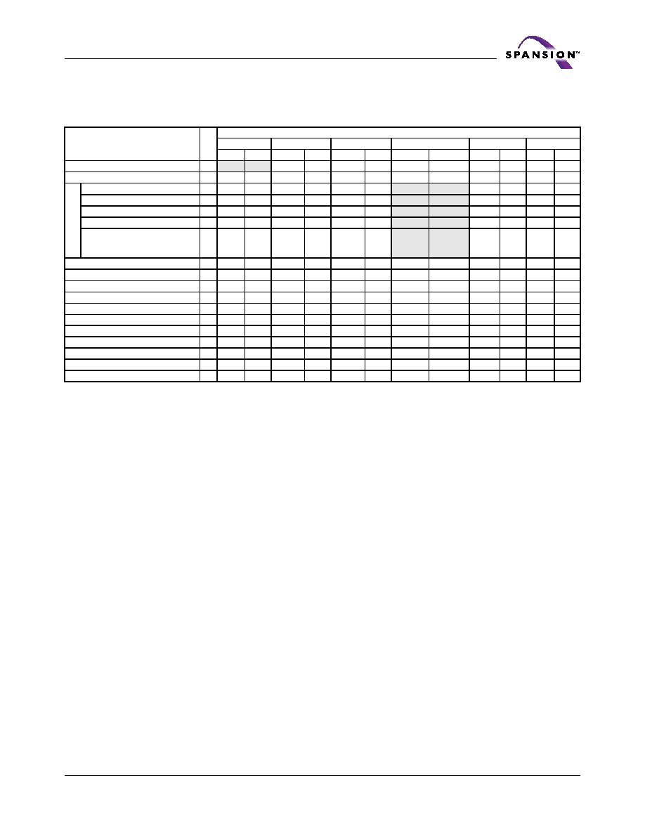
April 21, 2004 S29AL016M_00A4
S29AL016M
32
Command Definitions Tables
Table 10. Command Definitions (x16 Mode, BYTE# = V
IH
)
Legend:
X = Don't care
RA = Read Address of memory location to be read.
RD = Read Data read from location RA during read operation.
PA = Program Address. Addresses latch on falling edge of WE# or CE# pulse, whichever happens later.
PD = Program Data for location PA. Data latches on rising edge of WE# or CE# pulse, whichever happens first.
SA = Sector Address of sector to be verified (in autoselect mode) or erased. Address bits A19≠A15 uniquely select any sector.
Command
Sequence
(Note 1)
Cy
c
l
e
s
Bus Cycles (Notes 2≠5)
First
Second
Third
Fourth
Fifth
Sixth
Addr Data
Addr
Data
Addr
Data
Addr
Data
Addr
Data Addr Data
Read (Note 5)
1
RA
RD
Reset (Note 6)
1
XXX
F0
Au
to
se
le
ct
(N
o
t
e
7)
Manufacturer ID
4
555
AA
2AA
55
555
90
X00
0001
Device ID, Top Boot (Note 8)
6
555
AA
2AA
55
555
90
X01
22C4
Device ID, Bottom Boot (Note 8) 6
555
AA
2AA
55
555
90
X01
2249
SecSiTM Sector Factory Protect
4
555
AA
2AA
55
555
90
X41
(Note 9)
Sector Group Protect Verify
(Note 9)
4
555
AA
2AA
55
555
90
(SA)X02
00/01
Enter SecSi Sector Region
3
555
AA
2AA
55
555
88
Exit SecSi Sector Region
4
555
AA
2AA
55
555
90
XXX
00
Program
4
555
AA
2AA
55
555
A0
PA
PD
Unlock Bypass
3
555
AA
2AA
55
555
20
Unlock Bypass Program (Note 10)
2
XXX
A0
PA
PD
Unlock Bypass Reset (Note 11)
2
XXX
90
XXX
00
Chip Erase
6
555
AA
2AA
55
555
80
555
AA
2AA
55
555
10
Sector Erase
6
555
AA
2AA
55
555
80
555
AA
2AA
55
SA
30
Program/Erase Suspend (Note 12)
1
XXX
B0
Program/Erase Resume (Note 13)
1
XXX
30
CFI Query (Note 14)
1
55
98
Notes:
1. See Table
1
for description of bus operations.
2. All values are in hexadecimal.
3. Shaded cells indicate read cycles. All others are write
cycles.
4. During unlock and command cycles, when lower address
bits are 555 or 2AA as shown in table, address bits above
A11 and data bits above DQ7 are don't care.
5. No unlock or command cycles required when device is in
read mode.
6. Reset command is required to return to read mode (or to
erase-suspend-read mode if previously in Erase Suspend)
when device is in autoselect mode, or if DQ5 goes high
while device is providing status information.
7. Fourth cycle of the autoselect command sequence is a
read cycle. Data bits DQ15≠DQ8 are don't care. See
Autoselect Command Sequence
section for more
information.
8. Device ID must be read in three cycles.
9. Data is 00h for an unprotected sector group and 01h for a
protected sector group.
10. Unlock Bypass command is required prior to Unlock
Bypass Program command.
11. Unlock Bypass Reset command is required to return to
read mode when device is in unlock bypass mode.
12. System may read and program in non-erasing sectors, or
enter autoselect mode, when in Erase Suspend mode.
Erase Suspend command is valid only during a sector
erase operation.
13. Erase Resume command is valid only during Erase
Suspend mode.
14. Command is valid when device is ready to read array data
or when device is in autoselect mode.
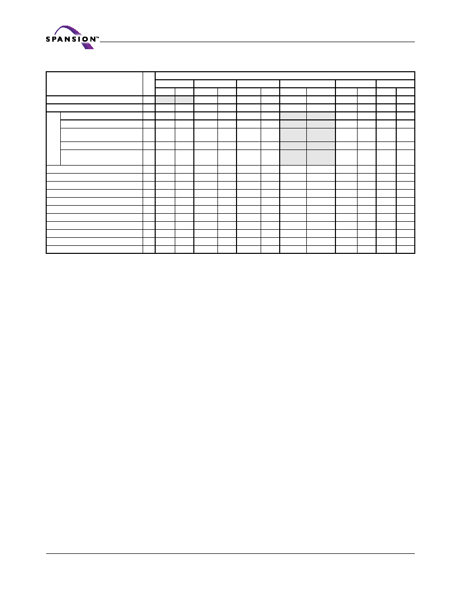
33
S29AL016M
S29AL016M_00A4 April 21, 2004
Table 11. Command Definitions (x8 Mode, BYTE# = V
IL
)
Legend:
X = Don't care
RA = Read Address of memory location to be read.
RD = Read Data read from location RA during read operation.
PA = Program Address. Addresses latch on falling edge of WE# or CE# pulse, whichever happens later.
PD = Program Data for location PA. Data latches on rising edge of WE# or CE# pulse, whichever happens first.
SA = Sector Address of sector to be verified (in autoselect mode) or erased. Address bits A19≠A15 uniquely select any sector.
Command
Sequence
(Note 1)
Cyc
l
e
s
Bus Cycles (Notes 2≠5)
First
Second
Third
Fourth
Fifth
Sixth
Addr Data
Addr
Data
Addr
Data
Addr
Data
Addr
Data Addr Data
Read (Note 5)
1
RA
RD
Reset (Note 6)
1
XXX
F0
Au
to
s
e
l
e
ct
(N
o
t
e
7
)
Manufacturer ID
4
AAA
AA
555
55
AAA
90
X00
01
Device ID, Top Boot (Note 8)
6
AAA
AA
555
55
AAA
90
X02
C4
Device ID, Bottom Boot (Note
8)
6
AAA
AA
555
55
AAA
90
X02
49
SecSiTM Sector Factory Protect
4
AAA
AA
555
55
AAA
90
X44
(Note 9)
Sector Group Protect Verify
(Note 9)
4
AAA
AA
555
55
AAA
90
(SA)X04
00/01
Enter SecSi Sector Region
3
AAA
AA
555
55
AAA
88
Exit SecSi Sector Region
4
AAA
AA
555
55
AAA
90
XXX
00
Program
4
AAA
AA
555
55
AAA
A0
PA
PD
Unlock Bypass
3
AAA
AA
555
55
AAA
20
Unlock Bypass Program (Note 10)
2
XXX
A0
PA
PD
Unlock Bypass Reset (Note 11)
2
XXX
90
XXX
00
Chip Erase
6
AAA
AA
555
55
AAA
80
AAA
AA
555
55
AAA
10
Sector Erase
6
AAA
AA
555
55
AAA
80
AAA
AA
555
55
SA
30
Program/Erase Suspend (Note 12)
1
XXX
B0
Program/Erase Resume (Note 13)
1
XXX
30
CFI Query (Note 14)
1
AA
98
Notes:
1. See Table
1
for description of bus operations.
2. All values are in hexadecimal.
3. Shaded cells indicate read cycles. All others are write
cycles.
4. During unlock and command cycles, when lower address
bits are 555 or AAA as shown in table, address bits above
A11 are don't care.
5. No unlock or command cycles required when device is in
read mode.
6. Reset command is required to return to read mode (or to
erase-suspend-read mode if previously in Erase Suspend)
when device is in autoselect mode, or if DQ5 goes high
while device is providing status information.
7. Fourth cycle of autoselect command sequence is a read
cycle. Data bits DQ15≠DQ8 are don't care. See
Autoselect
Command Sequence
section or more information.
8. Device ID must be read in three cycles.
9. Data is 00h for an unprotected sector group and 01h for a
protected sector group.
10. Unlock Bypass command is required prior to Unlock
Bypass Program command.
11. Unlock Bypass Reset command is required to return to
read mode when device is in unlock bypass mode.
12. System may read and program in non-erasing sectors, or
enter autoselect mode, when in Erase Suspend mode.
Erase Suspend command is valid only during a sector
erase operation.
13. Erase Resume command is valid only during Erase
Suspend mode.
14. Command is valid when device is ready to read array data
or when device is in autoselect mode.

April 21, 2004 S29AL016M_00A4
S29AL016M
34
Write Operation Status
The device provides several bits to determine the status of a write operation:
DQ2, DQ3, DQ5, DQ6, DQ7, and RY/BY#. Table
12
and the following subsections
describe the functions of these bits. DQ7, RY/BY#, and DQ6 each offer a method
for determining whether a program or erase operation is complete or in progress.
These three bits are discussed first.
DQ7: Data# Polling
The Data# Polling bit, DQ7, indicates to the host system whether an Embedded
Algorithm is in progress or completed, or whether the device is in Erase Suspend.
Data# Polling is valid after the rising edge of the final WE# pulse in the program
or erase command sequence.
During the Embedded Program algorithm, the device outputs on DQ7 the com-
plement of the datum programmed to DQ7. This DQ7 status also applies to
programming during Erase Suspend. When the Embedded Program algorithm is
complete, the device outputs the datum programmed to DQ7. The system must
provide the program address to read valid status information on DQ7. If a pro-
gram address falls within a protected sector, Data# Polling on DQ7 is active for
approximately 1 µs, then the device returns to reading array data.
During the Embedded Erase algorithm, Data# Polling produces a "0" on DQ7.
When the Embedded Erase algorithm is complete, or if the device enters the
Erase Suspend mode, Data# Polling produces a "1" on DQ7. This is analogous to
the complement/true datum output described for the Embedded Program algo-
rithm: the erase function changes all the bits in a sector to "1"; prior to this, the
device outputs the "complement," or "0." The system must provide an address
within any of the sectors selected for erasure to read valid status information on
DQ7.
After an erase command sequence is written, if all sectors selected for erasing
are protected, Data# Polling on DQ7 is active for approximately 100 µs, then the
device returns to reading array data. If not all selected sectors are protected, the
Embedded Erase algorithm erases the unprotected sectors, and ignores the se-
lected sectors that are protected.
When the system detects DQ7 has changed from the complement to true data,
it can read valid data at DQ7≠DQ0 on the following read cycles. This is because
DQ7 may change asynchronously with DQ0≠DQ6 while Output Enable (OE#) is
asserted low.
Figure 19
, Data# Polling Timings (During Embedded Algorithms),
in the
"AC Characteristics"
section illustrates this.
Table
12
shows the outputs for Data# Polling on DQ7.
Figure 7
shows the Data#
Polling algorithm.

35
S29AL016M
S29AL016M_00A4 April 21, 2004
Notes:
1. VA = Valid address for programming. During a sector erase operation, a valid
address is an address within any sector selected for erasure. During chip erase, a
valid address is any non-protected sector address.
2. DQ7 should be rechecked even if DQ5 = "1" because DQ7 may change simulta-
neously with DQ5.
Figure 7. Data# Polling Algorithm
RY/BY#: Ready/Busy#
The RY/BY# is a dedicated, open-drain output pin that indicates whether an Em-
bedded Algorithm is in progress or complete. The RY/BY# status is valid after the
rising edge of the final WE# pulse in the command sequence. Since RY/BY# is an
open-drain output, several RY/BY# pins can be tied together in parallel with a
pull-up resistor to V
CC
.
DQ7 = Data?
Yes
No
No
DQ5 = 1?
No
Yes
Yes
FAIL
PASS
Read DQ7≠DQ0
Addr = VA
Read DQ7≠DQ0
Addr = VA
DQ7 = Data?
START

April 21, 2004 S29AL016M_00A4
S29AL016M
36
If the output is low (Busy), the device is actively erasing or programming. (This
includes programming in the Erase Suspend mode.) If the output is high (Ready),
the device is ready to read array data (including during the Erase Suspend
mode), or is in the standby mode.
Table
12
shows the outputs for RY/BY#. Figures
13
,
14
,
17
and
18
show RY/BY#
for read, reset, program, and erase operations, respectively.
DQ6: Toggle Bit I
Toggle Bit I on DQ6 indicates whether an Embedded Program or Erase algorithm
is in progress or complete, or whether the device has entered the Erase Suspend
mode. Toggle Bit I may be read at any address, and is valid after the rising edge
of the final WE# pulse in the command sequence (prior to the program or erase
operation), and during the sector erase time-out.
During an Embedded Program or Erase algorithm operation, successive read cy-
cles to any address cause DQ6 to toggle. (The system may use either OE# or CE#
to control the read cycles.) When the operation is complete, DQ6 stops toggling.
After an erase command sequence is written, if all sectors selected for erasing
are protected, DQ6 toggles for approximately 100 µs, then returns to reading
array data. If not all selected sectors are protected, the Embedded Erase algo-
rithm erases the unprotected sectors, and ignores the selected sectors that are
protected.
The system can use DQ6 and DQ2 together to determine whether a sector is ac-
tively erasing or is erase-suspended. When the device is actively erasing (that is,
the Embedded Erase algorithm is in progress), DQ6 toggles. When the device en-
ters the Erase Suspend mode, DQ6 stops toggling. However, the system must
also use DQ2 to determine which sectors are erasing or erase-suspended. Alter-
natively, the system can use DQ7 (see the subsection on
"DQ7: Data# Polling"
).
If a program address falls within a protected sector, DQ6 toggles for approxi-
mately 1 µs after the program command sequence is written, then returns to
reading array data.
DQ6 also toggles during the erase-suspend-program mode, and stops toggling
once the Embedded Program algorithm is complete.
Table
12
shows the outputs for Toggle Bit I on DQ6.
Figure 8
shows the toggle bit
algorithm in flowchart form, and the section
"Reading Toggle Bits DQ6/DQ2"
ex-
plains the algorithm.
Figure 20
in the
"AC Characteristics"
section shows the
toggle bit timing diagrams.
Figure 21
shows the differences between DQ2 and
DQ6 in graphical form. See also the subsection on
"DQ2: Toggle Bit II"
.
DQ2: Toggle Bit II
The "Toggle Bit II" on DQ2, when used with DQ6, indicates whether a particular
sector is actively erasing (that is, the Embedded Erase algorithm is in progress),
or whether that sector is erase-suspended. Toggle Bit II is valid after the rising
edge of the final WE# pulse in the command sequence.
DQ2 toggles when the system reads at addresses within those sectors that have
been selected for erasure. (The system may use either OE# or CE# to control the
read cycles.) But DQ2 cannot distinguish whether the sector is actively erasing or
is erase-suspended. DQ6, by comparison, indicates whether the device is actively
erasing, or is in Erase Suspend, but cannot distinguish which sectors are selected
for erasure. Thus, both status bits are required for sector and mode information.
Refer to Table
12
to compare outputs for DQ2 and DQ6.

37
S29AL016M
S29AL016M_00A4 April 21, 2004
Figure 8
shows the toggle bit algorithm in flowchart form, and the section
"Read-
ing Toggle Bits DQ6/DQ2"
explains the algorithm. See also the
DQ6: Toggle Bit I
subsection.
Figure 20
shows the toggle bit timing diagram.
Figure 21
shows the
differences between DQ2 and DQ6 in graphical form.
Reading Toggle Bits DQ6/DQ2
Refer to
Figure 8
for the following discussion. Whenever the system initially be-
gins reading toggle bit status, it must read DQ7≠DQ0 at least twice in a row to
determine whether a toggle bit is toggling. Typically, the system would note
and store the value of the toggle bit after the first read. After the second read,
the system would compare the new value of the toggle bit with the first. If the
toggle bit is not toggling, the device has completed the program or erase op-
eration. The system can read array data on DQ7≠DQ0 on the following read
cycle.
However, if after the initial two read cycles, the system determines that the toggle
bit is still toggling, the system also should note whether the value of DQ5 is high
(see the section on DQ5). If it is, the system should then determine again
whether the toggle bit is toggling, since the toggle bit may have stopped toggling
just as DQ5 went high. If the toggle bit is no longer toggling, the device has suc-
cessfully completed the program or erase operation. If it is still toggling, the
device did not complete the operation successfully, and the system must write
the reset command to return to reading array data.
The remaining scenario is that the system initially determines that the toggle bit
is toggling and DQ5 has not gone high. The system may continue to monitor the
toggle bit and DQ5 through successive read cycles, determining the status as de-
scribed in the previous paragraph. Alternatively, it may choose to perform other
system tasks. In this case, the system must start at the beginning of the algo-
rithm when it returns to determine the status of the operation (top of
Figure 8
).
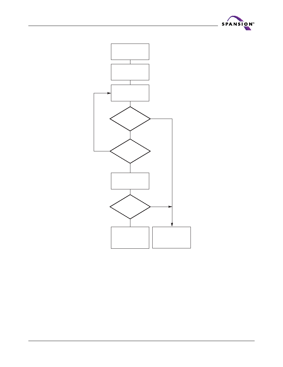
April 21, 2004 S29AL016M_00A4
S29AL016M
38
Figure 8. Toggle Bit Algorithm
Notes:
1. Read toggle bit twice to determine whether or not it is toggling. See text.
2. Recheck toggle bit because it may stop toggling as DQ5 changes to "1". See text.
DQ5: Exceeded Timing Limits
DQ5 indicates whether the program or erase time has exceeded a specified inter-
nal pulse count limit. Under these conditions DQ5 produces a "1." This is a failure
condition that indicates the program or erase cycle was not successfully
completed.
The DQ5 failure condition may appear if the system tries to program a "1" to a
location that is previously programmed to "0." Only an erase operation can
START
No
Yes
Yes
DQ5 = 1?
No
Yes
Toggle Bit
= Toggle?
No
Program/Erase
Operation Not
Complete, Write
Reset Command
Program/Erase
Operation Complete
Read DQ7≠DQ0
Toggle Bit
= Toggle?
Read DQ7≠DQ0
Twice
Read DQ7≠DQ0
(Note 1)
(Notes
1, 2)
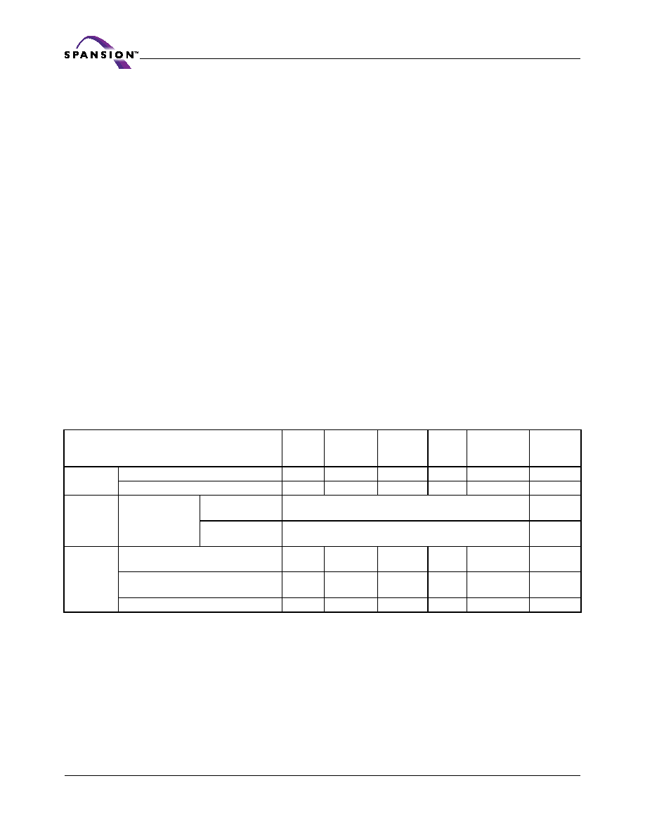
39
S29AL016M
S29AL016M_00A4 April 21, 2004
change a "0" back to a "1." Under this condition, the device halts the opera-
tion, and when the operation has exceeded the timing limits, DQ5 produces a "1."
Under both these conditions, the system must issue the reset command to return
the device to reading array data.
DQ3: Sector Erase Timer
After writing a sector erase command sequence, the system may read DQ3 to de-
termine whether or not an erase operation has begun. (The sector erase timer
does not apply to the chip erase command.) If additional sectors are selected for
erasure, the entire time-out also applies after each additional sector erase com-
mand. When the time-out is complete, DQ3 switches from "0" to "1." The system
may ignore DQ3 if the system can guarantee that the time between additional
sector erase commands will always be less than 50 µs. See also the
"Sector
Erase Command Sequence"
section.
After the sector erase command sequence is written, the system should read the
status on DQ7 (Data# Polling) or DQ6 (Toggle Bit I) to ensure the device has ac-
cepted the command sequence, and then read DQ3. If DQ3 is "1", the internally
controlled erase cycle has begun; all further commands (other than Erase Sus-
pend) are ignored until the erase operation is complete. If DQ3 is "0", the device
will accept additional sector erase commands. To ensure the command has been
accepted, the system software should check the status of DQ3 prior to and fol-
lowing each subsequent sector erase command. If DQ3 is high on the second
status check, the last command might not have been accepted. Table
12
shows
the outputs for DQ3.
Table 12. Write Operation Status
Notes:
1. DQ5 switches to `1' when an Embedded Program or Embedded Erase operation has exceeded the maximum timing
limits. See
"DQ5: Exceeded Timing Limits"
for more information.
2. DQ7 and DQ2 require a valid address when reading status information. Refer to the appropriate subsection for further
details.
Operation
DQ7
(Note
2)
DQ6
DQ5
(Note 1)
DQ3
DQ2
(Note 2)
RY/BY#
Standard
Mode
Embedded Program Algorithm
DQ7#
Toggle
0
N/A
No toggle
0
Embedded Erase Algorithm
0
Toggle
0
1
Toggle
0
Program
Suspend
Mode
Program-
Suspend Read
Program-
Suspended Sector
Invalid (not allowed)
1
Non-Program
Suspended Sector
Data
1
Erase
Suspend
Mode
Reading within Erase
Suspended Sector
1
No toggle
0
N/A
Toggle
1
Reading within Non-Erase Suspended
Sector
Data
Data
Data
Data
Data
1
Erase-Suspend-Program
DQ7#
Toggle
0
N/A
N/A
0
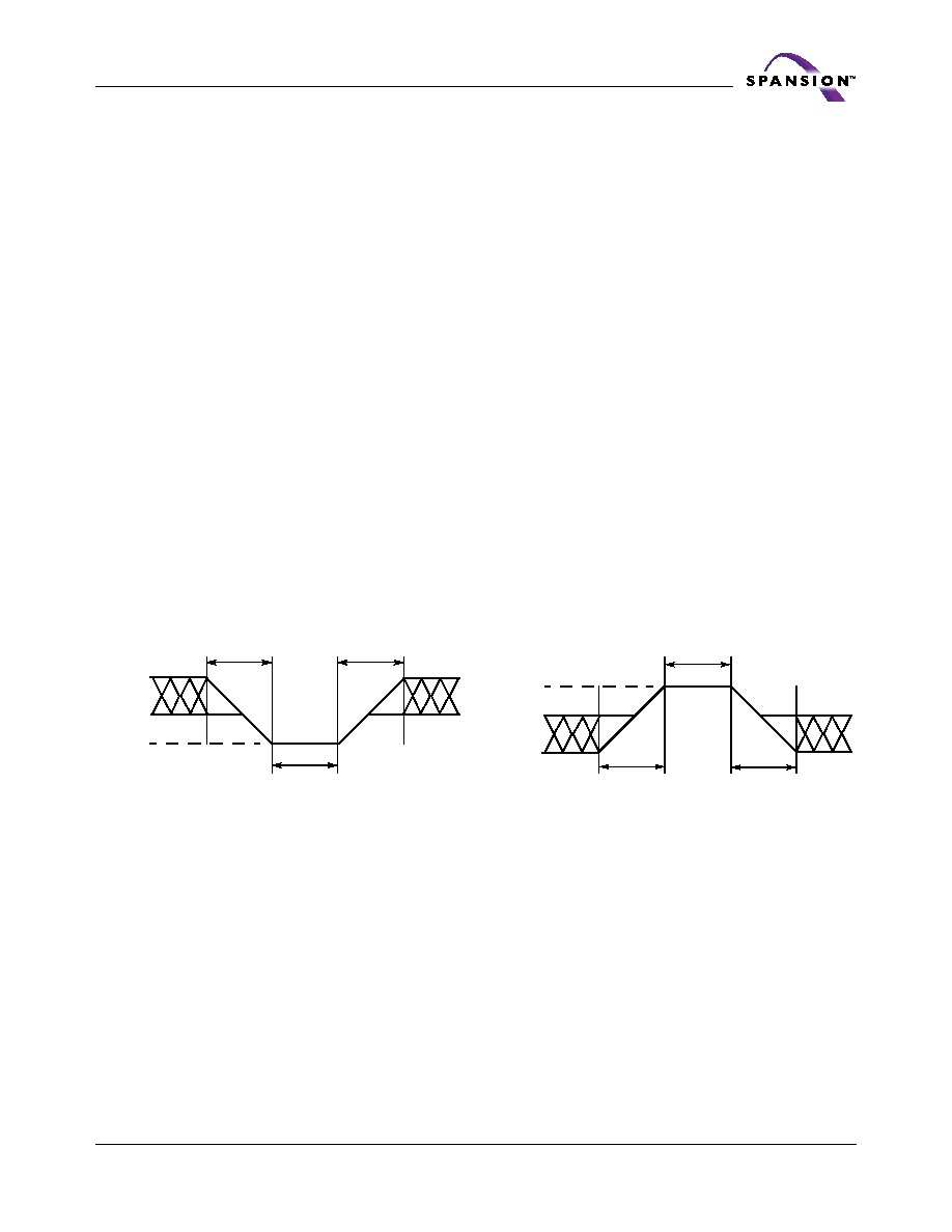
April 21, 2004 S29AL016M_00A4
S29AL016M
40
Absolute Maximum Ratings
Storage Temperature, Plastic Packages. . . . . . . . . . . . . . . . .≠65∞C to +150∞C
Ambient Temperature with Power Applied . . . . . . . . . . . . . . .≠65∞C to +125∞C
Voltage with Respect to Ground
V
CC
(Note 1). . . . . . . . . . . . . . . . . . . . . . . . . . . . . . .≠0.5 V to +4.0 V
A9, OE#, and RESET# (Note 2) . . . . . . . . . . . . . . . . ≠0.5 V to +12.5 V
All other pins (Note 1) . . . . . . . . . . . . . . . . . . . . . ≠0.5 V to V
CC
+0.5 V
Output Short Circuit Current (Note 3). . . . . . . . . . . . . . . . . . . . . . . . 200 mA
Notes:
1. Minimum DC voltage on input or I/O pins is ≠0.5 V. During voltage transitions,
input or I/O pins may overshoot V
SS
to ≠2.0 V for periods of up to 20 ns. See
Figure
9
. Maximum DC voltage on input or I/O pins is V
CC
+0.5 V. During voltage
transitions, input or I/O pins may overshoot to V
CC
+2.0 V for periods up to 20 ns.
See
Figure 10
.
2. Minimum DC input voltage on pins A9, OE#, and RESET# is -0.5 V. During voltage
transitions, A9, OE#, and RESET# may overshoot V
SS
to ≠2.0 V for periods of up
to 20 ns. See
Figure 9
. Maximum DC input voltage on pin A9 is +12.5 V which
may overshoot to 14.0 V for periods up to 20 ns.
3. No more than one output may be shorted to ground at a time. Duration of the short
circuit should not be greater than one second.
Stresses above those listed under "Absolute Maximum Ratings" may cause permanent
damage to the device. This is a stress rating only; functional operation of the device
at these or any other conditions above those indicated in the operational sections of
this data sheet is not implied. Exposure of the device to absolute maximum rating con-
ditions for extended periods may affect device reliability.
Operating Ranges
Industrial (I) Devices
Ambient Temperature (T
A
) . . . . . . . . . . . . . . . . . . . . . . . . . ≠40∞C to +85∞C
V
CC
Supply Voltages
V
CC
for full voltage range . . . . . . . . . . . . . . . . . . . . . . . . . . . . 2.7 V to 3.6 V
V
CC
for regulated range . . . . . . . . . . . . . . . . . . . . . . . . . . . . . 3.0 V to 3.6 V
Operating ranges define those limits between which the functionality of the device is
guaranteed.
Figure 9. Maximum Negative
Overshoot Waveform
Figure 10. Maximum Positive
Overshoot Waveform
20 ns
20 ns
+0.8 V
≠0.5 V
20 ns
≠2.0 V
20 ns
20 ns
V
CC
+2.0 V
V
CC
+0.5 V
20 ns
2.0 V
41
S29AL016M
S29AL016M_00A4 April 21, 2004
DC Characteristics
CMOS Compatible
Notes:
1. The I
CC
current listed is typically less than 2 mA/MHz, with OE# at V
IH
. Typical V
CC
is 3.0 V.
2. Maximum I
CC
specifications are tested with V
CC
= V
CC
max.
3. I
CC
active while Embedded Erase or Embedded Program is in progress.
4. At extended temperature range (>+85∞C), typical current is 5 µA and maximum current is 10 µA.
5. Automatic sleep mode enables the low power mode when addresses remain stable for t
ACC
+ 30 ns.
6. Not 100% tested.
7. V
CC
voltage requirements.
Parameter
Description
Test Conditions
Min
Typ
Max
Unit
I
LI
Input Load Current
V
IN
= V
SS
to V
CC
,
V
CC
= V
CC
max
±1.0
µA
I
LIT
A9 Input Load Current
V
CC
= V
CC max
; A9 = 12.5 V
35
µA
I
LR
Reset Leakage Current
V
CC
= V
CC max
; RESET# = 12.5 V
35
µA
I
LO
Output Leakage Current
V
OUT
= V
SS
to V
CC
,
V
CC
= V
CC max
±1.0
µA
CE# = V
IL,
OE#
=
V
IH,
Byte Mode
10 MHz
35
50
mA
I
CC1
V
CC
Active Read Current
(Notes 1, 2)
5 MHz
15
20
1 MHz
2.5
10
CE# = V
IL,
OE#
=
V
IH,
Word Mode
10 MHz
35
50
5 MHz
15
20
1 MHz
2.5
10
I
CC2
V
CC
Active Write Current
(Notes 2, 3, 5)
CE# = V
IL,
OE# = V
IH
40
60
mA
I
CC3
V
CC
Standby Current (Notes 2, 4) CE#, RESET# = V
CC
± 0.3 V
0.4
5
µA
I
CC4
V
CC
Standby Current During Reset
(Notes 2, 4)
RESET# = V
SS
± 0.3 V
0.8
5
µA
I
CC5
Automatic Sleep Mode
(Notes 2, 4, 6)
V
IH
= V
CC
± 0.3 V;
-0.1 < V
IL
0.3 V
0.4
5
µA
V
IL
Input Low Voltage (Notes 6, 7)
-0.5
0.6
V
V
IH
Input High Voltage (Notes 6, 7)
0.7 V
CC
V
CC
+ 0.5
V
V
ID
Voltage for Autoselect and
Temporary Sector Unprotect
V
CC
= 3.3 V
11.5
12.5
V
V
OL
Output Low Voltage
I
OL
= 4.0 mA, V
CC
= V
CC min
0.45
V
V
OH1
Output High Voltage
I
OH
= -2.0 mA, V
CC
= V
CC min
0.85 x V
CC
V
V
OH2
I
OH
= -100 µA, V
CC
= V
CC min
V
CC
≠0.4
V
LKO
Low V
CC
Lock-Out Voltage (Note 4)
2.3
2.5
V
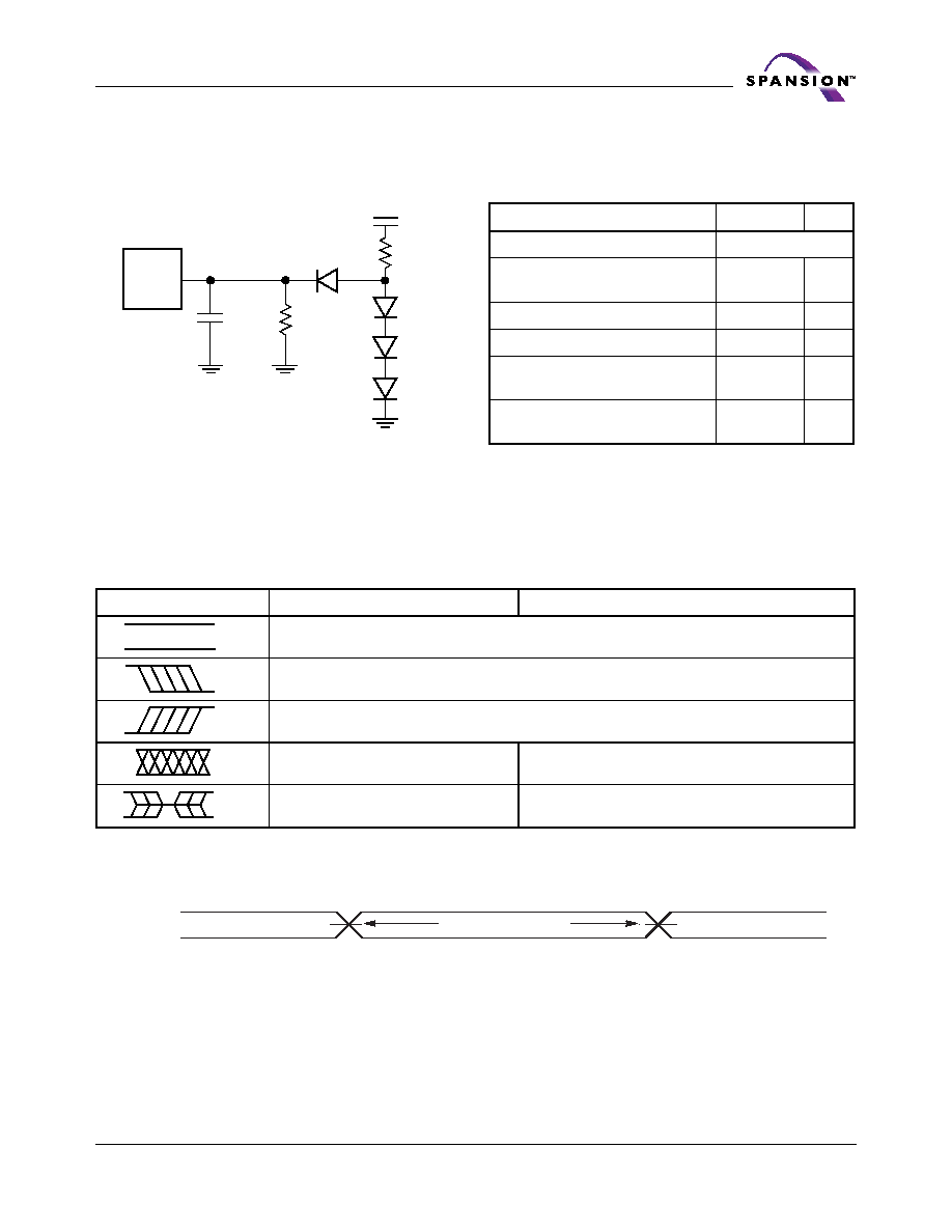
April 21, 2004 S29AL016M_00A4
S29AL016M
42
Test Conditions
Key to Switching Waveforms
Figure 12. Input Waveforms and Measurement Levels
Note: Diodes are IN3064 or equivalent
Figure 11. Test Setup
Table 13. Test Specifications
2.7 k
CL
6.2 k
3.3 V
Device
Under
Test
Test Condition
90, 100
Unit
Output Load
1 TTL gate
Output Load Capacitance, C
L
(including jig capacitance)
30
pF
Input Rise and Fall Times
5
ns
Input Pulse Levels
0.0 or V
CC
V
Input timing measurement
reference levels
0.5 V
CC
V
Output timing measurement
reference levels
0.5 V
CC
V
WAVEFORM
INPUTS
OUTPUTS
Steady
Changing from H to L
Changing from L to H
Don't Care, Any Change Permitted
Changing, State Unknown
Does Not Apply
Center Line is High Impedance State (High Z)
V
CC
0.0 V
0.5 V
CC
Output
Measurement Level
Input
0.5 V
CC
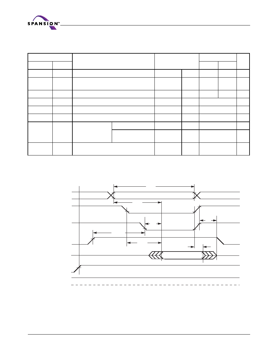
43
S29AL016M
S29AL016M_00A4 April 21, 2004
AC Characteristics
Read Operations
Notes:
1. Not 100% tested.
2. See
Figure 11
and Table
13
for test specifications.
Figure 13. Read Operations Timings
Parameter
Description
Speed Options
JEDEC
Std
Test Setup
90
100
Unit
t
AVAV
t
RC
Read Cycle Time (Note 1)
Min
90
100
ns
t
AVQV
t
ACC
Address to Output Delay
CE# = V
IL
OE# = V
IL
Max
90
100
ns
t
ELQV
t
CE
Chip Enable to Output Delay
OE# = V
IL
Max
90
100
ns
t
GLQV
t
OE
Output Enable to Output Delay
Max
25
ns
t
EHQZ
t
DF
Chip Enable to Output High Z (Note 1)
Max
20
ns
t
GHQZ
t
DF
Output Enable to Output High Z (Note 1)
Max
20
ns
t
OEH
Output Enable
Hold Time (Note 1)
Read
Min
0
ns
Toggle and
Data# Polling
Min
10
ns
t
AXQX
t
OH
Output Hold Time From Addresses, CE# or
OE#, Whichever Occurs First (Note 1)
Min
0
ns
t
CE
Outputs
WE#
Addresses
CE#
OE#
HIGH Z
Output Valid
HIGH Z
Addresses Stable
t
RC
t
ACC
t
OEH
t
OE
0 V
RY/BY#
RESET#
t
DF
t
OH

April 21, 2004 S29AL016M_00A4
S29AL016M
44
AC Characteristics
Hardware Reset (RESET#)
Note: Not 100% tested.
Figure 14. RESET# Timings
Parameter
Description
All Speed Options
JEDEC
Std
Test
Setup
Unit
t
READY
RESET# Pin Low (During Embedded Algorithms) to
Read or Write (See Note)
Max
20
µs
t
READY
RESET# Pin Low (NOT During Embedded Algorithms)
to Read or Write (See Note)
Max
500
ns
t
RP
RESET# Pulse Width
Min
500
ns
t
RH
RESET# High Time Before Read (See Note)
Min
50
ns
t
RPD
RESET# Low to Standby Mode
Min
20
µs
t
RB
RY/BY# Recovery Time
Min
0
ns
RESET#
RY/BY#
RY/BY#
t
RP
t
Ready
Reset Timings NOT during Embedded Algorithms
t
Ready
CE#, OE#
t
RH
CE#, OE#
Reset Timings during Embedded Algorithms
RESET#
t
RP
t
RB
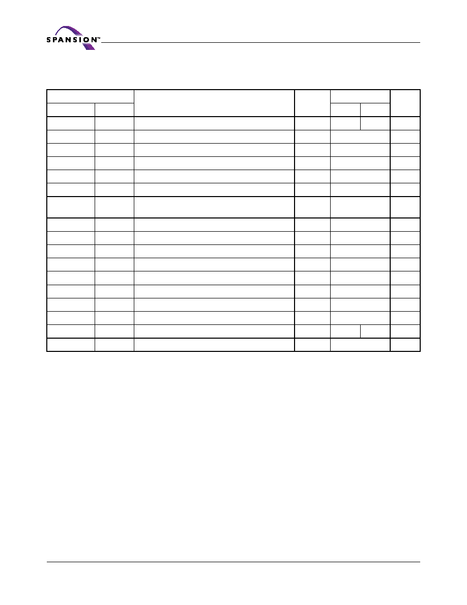
45
S29AL016M
S29AL016M_00A4 April 21, 2004
AC Characteristics
Erase/Program Operations
Notes:
1. Not 100% tested.
2. See the
"Erase and Programming Performance"
section for more information.
3. If a program suspend command is issued within t
POLL
, the device requires t
POLL
before reading status data, once
programming has resumed (that is, the program resume command has been written). If the suspend command was issued
after t
POLL
, status data is available immediately after programming has resumed. See Figure 15.
Parameter
Speed Options
JEDEC
Std
Description
90
100
Unit
t
AVAV
t
WC
Write Cycle Time (Note 1)
Min
90
100
ns
t
AVWL
t
AS
Address Setup Time
Min
0
ns
t
WLAX
t
AH
Address Hold Time
Min
45
ns
t
DVWH
t
DS
Data Setup Time
Min
35
ns
t
WHDX
t
DH
Data Hold Time
Min
0
ns
t
OES
Output Enable Setup Time
Min
0
ns
t
GHWL
t
GHWL
Read Recovery Time Before Write
(OE# High to WE# Low)
Min
0
ns
t
ELWL
t
CS
CE# Setup Time
Min
0
ns
t
WHEH
t
CH
CE# Hold Time
Min
0
ns
t
WLWH
t
WP
Write Pulse Width
Min
35
ns
t
WHWL
t
WPH
Write Pulse Width High
Min
30
ns
t
WHWH1
t
WHWH1
Programming Operation (Note 2)
Typ
18
µs
t
WHWH2
t
WHWH2
Sector Erase Operation (Note 2)
Typ
1
sec
t
VCS
V
CC
Setup Time (Note 1)
Min
50
µs
t
RB
Recovery Time from RY/BY#
Min
0
ns
t
BUSY
Program/Erase Valid to RY/BY# Delay
Max
90
100
ns
t
POLL
Program Valid Before Status Polling (Note 3)
Max
4
µs
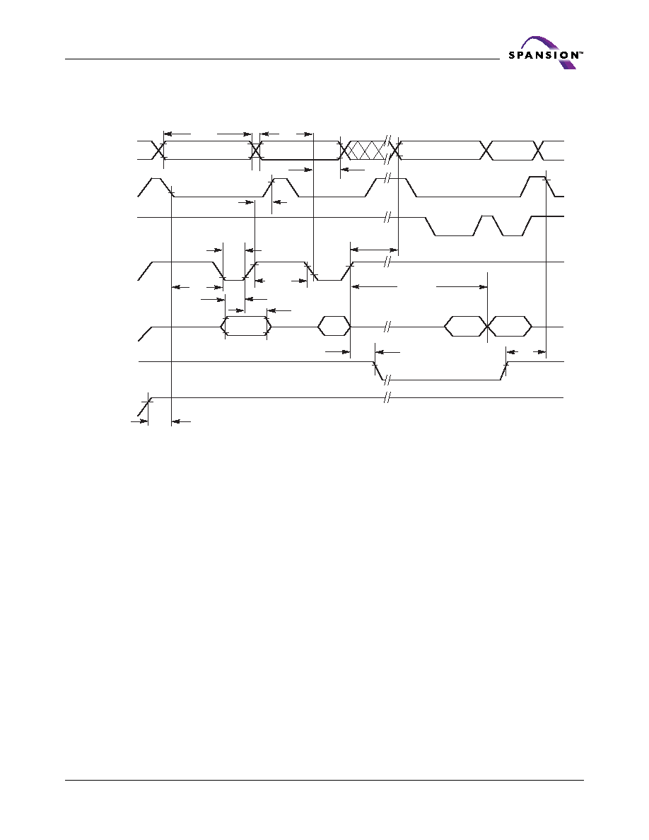
April 21, 2004 S29AL016M_00A4
S29AL016M
46
AC Characteristics
Notes:
1. PA = program address, PD = program data, D
OUT
is the true data at the program address.
2. Illustration shows device in word mode.
Figure 15. Program Operation Timings
OE#
WE#
CE#
V
CC
Data
Addresses
t
DS
t
AH
t
DH
t
WP
PD
t
WHWH1
t
WC
t
AS
t
WPH
t
VCS
555h
PA
PA
Read Status Data (last two cycles)
A0h
t
CS
Status
D
OUT
Program Command Sequence (last two cycles)
RY/BY#
t
RB
t
BUSY
t
CH
PA
t
POLL
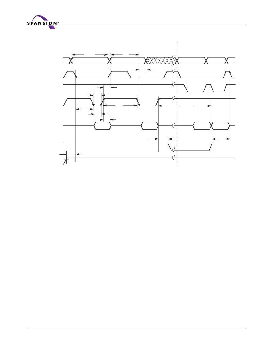
47
S29AL016M
S29AL016M_00A4 April 21, 2004
AC Characteristics
Notes:
1. SA = sector address (for Sector Erase), VA = Valid Address for reading status data (see "Write Operation Status").
2. Illustration shows device in word mode.
Figure 16. Chip/Sector Erase Operation Timings
OE#
CE#
Addresses
V
CC
WE#
Data
2AAh
SA
t
AH
t
WP
t
WC
t
AS
t
WPH
555h for chip erase
10 for Chip Erase
30h
t
DS
t
VCS
t
CS
t
DH
55h
t
CH
In
Progress
Complete
t
WHWH2
VA
VA
Erase Command Sequence (last two cycles)
Read Status Data
RY/BY#
t
RB
t
BUSY
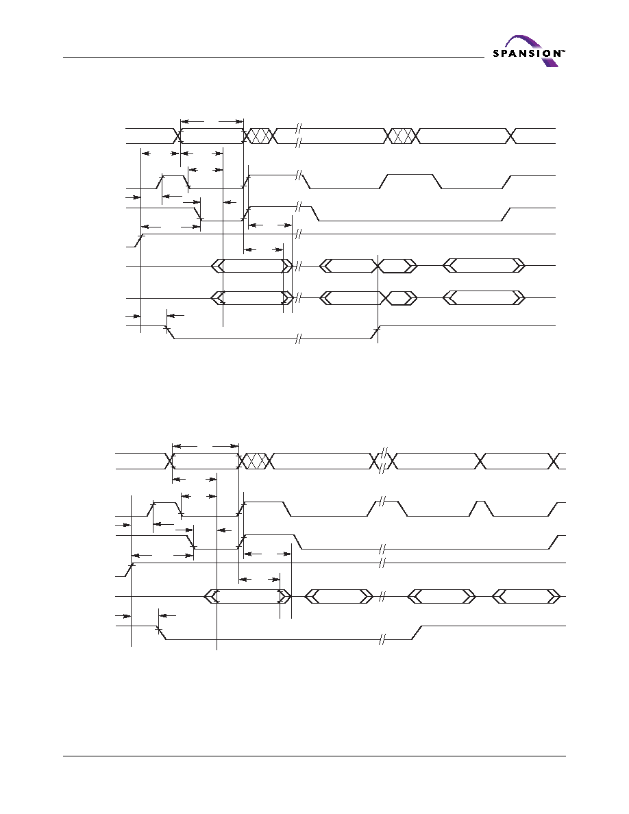
April 21, 2004 S29AL016M_00A4
S29AL016M
48
AC Characteristics
Note: VA = Valid address. Illustration shows first status cycle after command sequence, last status read cycle, and array
data read cycle.
Figure 17. Data# Polling Timings
(During Embedded Algorithms)
Note: VA = Valid address; not required for DQ6. Illustration shows first two status cycle after command sequence, last
status read cycle, and array data read cycle.
Figure 18. Toggle Bit Timings
(During Embedded Algorithms)
WE#
CE#
OE#
High Z
t
OE
High Z
DQ7
DQ0≠DQ6
RY/BY#
t
BUSY
Complement
True
Addresses
VA
t
OEH
t
CE
t
CH
t
OH
t
DF
VA
VA
Status Data
Complement
Status Data
True
Valid Data
Valid Data
t
ACC
t
POLL
t
RC
WE#
CE#
OE#
High Z
t
OE
DQ6/DQ2
RY/BY#
t
BUSY
Addresses
VA
t
OEH
t
CE
t
CH
t
OH
t
DF
VA
VA
t
ACC
t
RC
Valid Data
Valid Status
Valid Status
(first read)
(second read)
(stops toggling)
Valid Status
VA
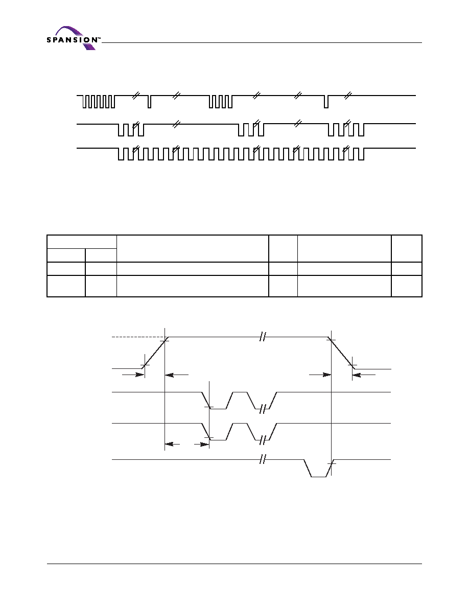
49
S29AL016M
S29AL016M_00A4 April 21, 2004
AC Characteristics
Note: The system may use CE# or OE# to toggle DQ2 and DQ6. DQ2 toggles only when read at an address within an
erase-suspended sector.
Figure 19. DQ2 vs. DQ6 for Erase and
Erase Suspend Operations
Temporary Sector Unprotect
Note: Not 100% tested.
Figure 20. Temporary Sector Unprotect/Timing Diagram
Parameter
All Speed Options
JEDEC
Std
Description
Unit
t
VIDR
V
ID
Rise and Fall Time (See Note)
Min
500
ns
t
RSP
RESET# Setup Time for Temporary Sector
Unprotect
Min
4
µs
Enter
Erase
Erase
Erase
Enter Erase
Suspend Program
Erase Suspend
Read
Erase Suspend
Read
Erase
WE#
DQ6
DQ2
Erase
Complete
Erase
Suspend
Suspend
Program
Resume
Embedded
Erasing
RESET#
t
VIDR
12 V
0 or 3 V
CE#
WE#
RY/BY#
t
VIDR
t
RSP
Program or Erase Command Sequence
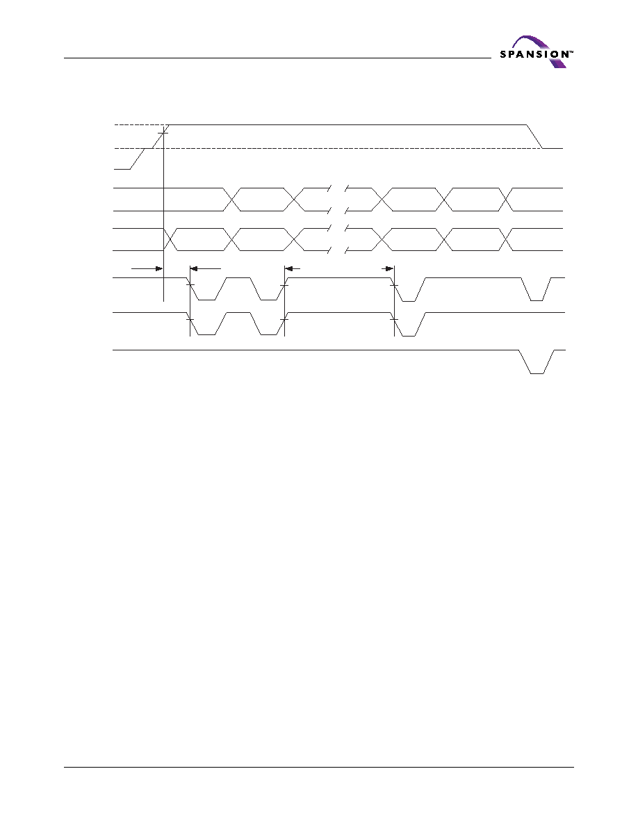
April 21, 2004 S29AL016M_00A4
S29AL016M
50
AC Characteristics
Note: For sector protect, A6 = 0, A1 = 1, A0 = 0. For sector unprotect, A6 = 1, A1 = 1, A0 = 0.
Figure 21. Sector Protect/Unprotect Timing Diagram
Sector Protect: 150 µs
Sector Unprotect: 15 ms
1 µs
RESET#
SA, A6,
A1, A0
Data
CE#
WE#
OE#
60h
60h
40h
Valid*
Valid*
Valid*
Status
Sector Protect/Unprotect
Verify
V
ID
V
IH

51
S29AL016M
S29AL016M_00A4 April 21, 2004
AC Characteristics
Alternate CE# Controlled Erase/Program Operations
Notes:
1. Not 100% tested.
2. See the
"Erase and Programming Performance"
section for more information.
3. If a program suspend command is issued within t
POLL
, the device requires t
POLL
before reading status data, once
programming has resumed (that is, the program resume command has been written). If the suspend command was issued
after t
POLL
, status data is available immediately after programming has resumed. See Figure 22.
Parameter
Speed Options
JEDEC
Std
Description
90
100
Unit
t
AVAV
t
WC
Write Cycle Time (Note 1)
Min
90
100
ns
t
AVEL
t
AS
Address Setup Time
Min
0
ns
t
ELAX
t
AH
Address Hold Time
Min
45
ns
t
DVEH
t
DS
Data Setup Time
Min
35
ns
t
EHDX
t
DH
Data Hold Time
Min
0
ns
t
OES
Output Enable Setup Time
Min
0
ns
t
GHEL
t
GHEL
Read Recovery Time Before Write
(OE# High to WE# Low)
Min
0
ns
t
WLEL
t
WS
WE# Setup Time
Min
0
ns
t
EHWH
t
WH
WE# Hold Time
Min
0
ns
t
ELEH
t
CP
CE# Pulse Width
Min
35
ns
t
EHEL
t
CPH
CE# Pulse Width High
Min
25
ns
t
WHWH1
t
WHWH1
Programming Operation (Note 2)
Typ
18
µs
t
WHWH2
t
WHWH2
Sector Erase Operation (Note 2)
Typ
0.7
sec
t
RH
RESET# High Time Before Write
Min
50
ns
t
POLL
Program Valid Before Status Polling
(Note 3)
Max
4
µs
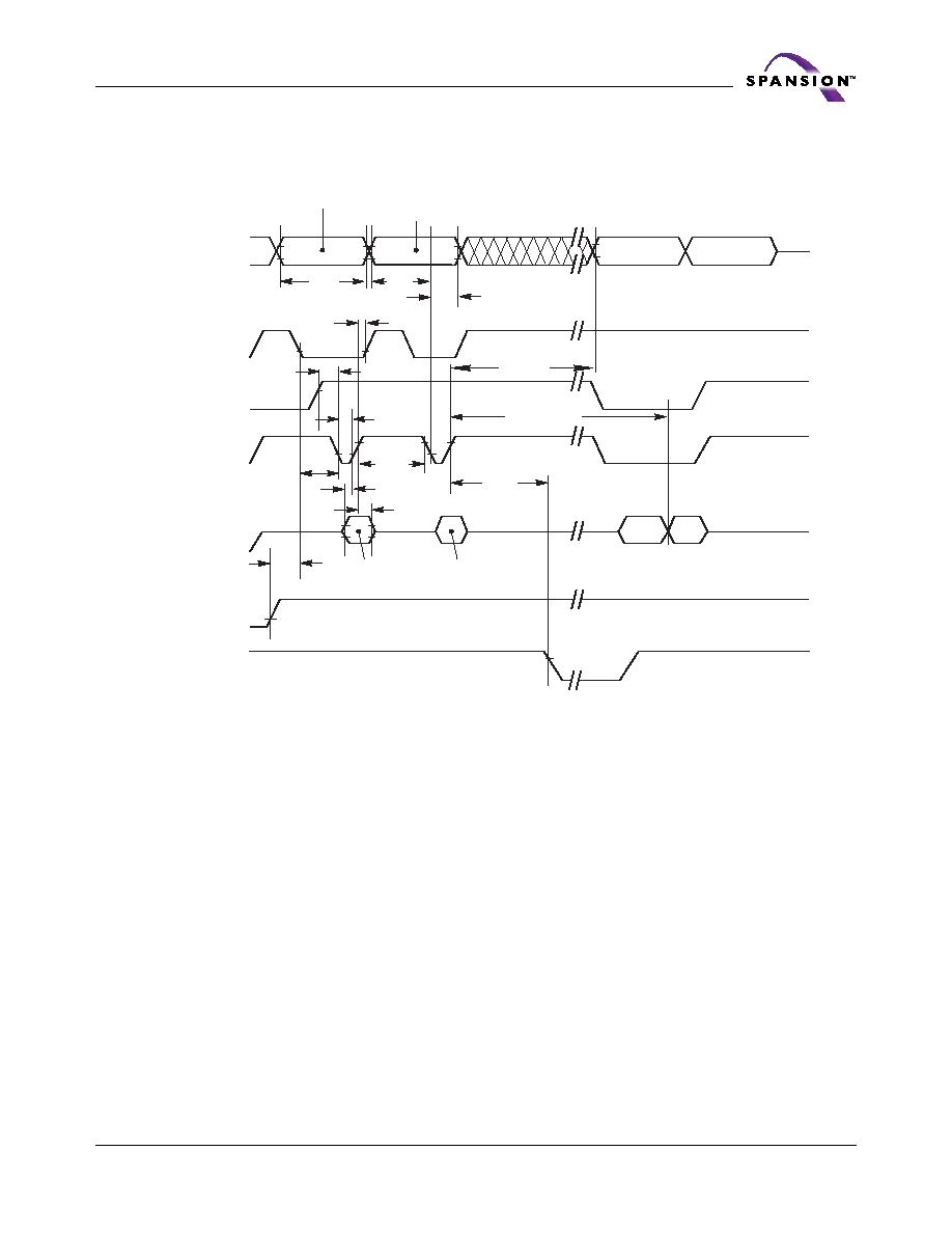
April 21, 2004 S29AL016M_00A4
S29AL016M
52
AC Characteristics
Notes:
1. PA = program address, PD = program data, DQ7# = complement of the data written to the device, D
OUT
= data written to
the device.
2. Figure indicates the last two bus cycles of the command sequence.
3. Word mode address used as an example.
Figure 22. Alternate CE# Controlled Write Operation Timings
t
GHEL
t
WS
OE#
CE#
WE#
RESET#
t
DS
Data
t
AH
Addresses
t
DH
t
CP
DQ7#,
D
OUT
t
WC
t
AS
t
CPH
PA
Data# Polling
A0 for program
55 for erase
t
RH
t
WHWH1 or 2
RY/BY#
t
WH
PD for program
30 for sector erase
10 for chip erase
555 for program
2AA for erase
PA for program
SA for sector erase
555 for chip erase
t
BUSY
DQ15
t
POLL

53
S29AL016M
S29AL016M_00A4 April 21, 2004
Erase and Programming Performance
Notes:
1. Typical program and erase times assume the following conditions: 25
∞
C, V
CC
= 3.0 V, 10,000 cycles, checkerboard data
pattern.
2. Under worst case conditions of 90∞C, V
CC
= 2.7 V, 100,000 cycles.
3. The typical chip programming time is considerably less than the maximum chip programming time listed, since most bytes
program faster than the maximum program times listed.
4. In the pre-programming step of the Embedded Erase algorithm, all bytes are programmed to 00h before erasure.
5. System-level overhead is the time required to execute the two- or four-bus-cycle sequence for the program command. See
Tables
2
≠
3
for further information on command definitions.
TSOP Pin and BGA Package Capacitance
Notes:
1. Sampled, not 100% tested.
2. Test conditions T
A
= 25∞C, f = 1.0 MHz.
Parameter
Typ (Note 1)
Max (Note 2)
Unit
Comments
Sector Erase Time
0.7
7.5
s
Excludes 00h programming
prior to erasure (Note 4)
Chip Erase Time
32
s
Byte Programming Time
18
µs
Word Programming Time
18
µs
Excludes system level
overhead (Note 5)
Chip Programming Time
(Note 3)
Byte Mode
36
s
Word Mode
19
s
Parameter Symbol
Parameter Description
Test Setup
Typ
Max
Unit
C
IN
Input Capacitance
V
IN
= 0
TSOP
6
7.5
pF
BGA
4.2
5.0
pF
C
OUT
Output Capacitance
V
OUT
= 0
TSOP
8.5
12
pF
BGA
5.4
6.5
pF
C
IN2
Control Pin Capacitance
V
IN
= 0
TSOP
7.5
9
pF
BGA
3.9
4.7
pF
April 21, 2004 S29AL016M_00A4
S29AL016M
54
Physical Dimensions
TS 048--48-Pin Standard TSOP
Note: BSC is an ANSI standard for Basic Space Centering.
Dwg rev AA; 10/99
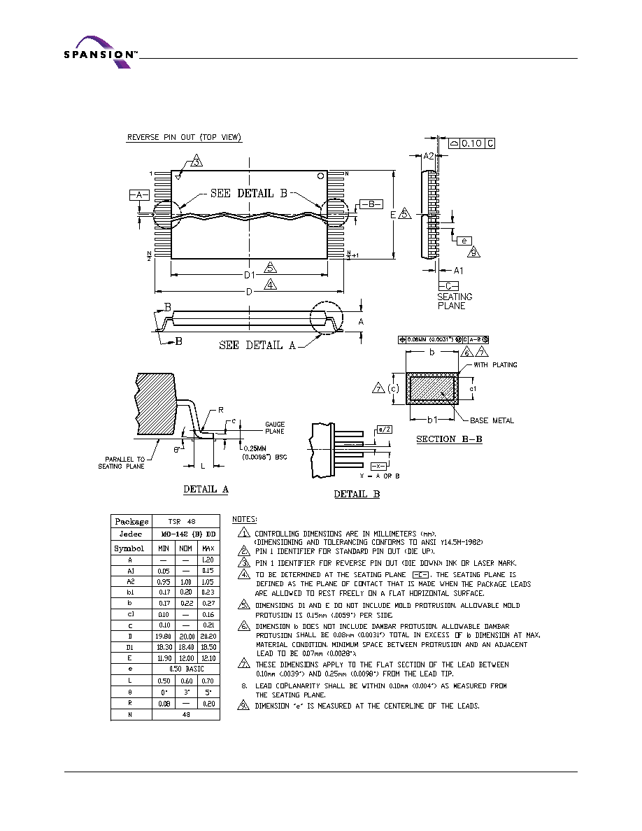
55
S29AL016M
S29AL016M_00A4 April 21, 2004
Physical Dimensions
TSR048--48-Pin Reverse TSOP
Note: BSC is an ANSI standard for Basic Space Centering.
Dwg rev AA; 10/99
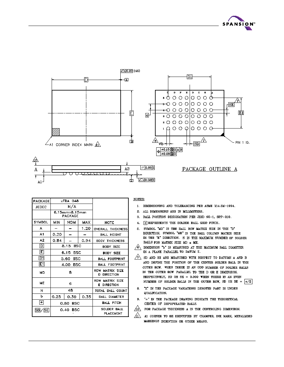
April 21, 2004 S29AL016M_00A4
S29AL016M
56
Physical Dimensions
FBA048--48-Ball Fine-Pitch Ball Grid Array (BGA)
6 x 8 mm Package
Note: BSC is an ANSI standard for Basic Space Centering.
Dwg rev AF; 10/99
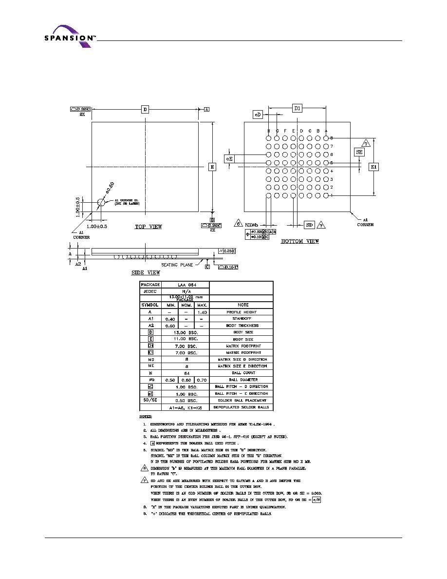
57
S29AL016M
S29AL016M_00A4 April 21, 2004
Physical Dimensions
LAA064--64-Ball Fortified Ball Grid Array (BGA)
13 x 11 mm Package
Note: BSC is an ANSI standard for Basic Space Centering.

April 21, 2004 S29AL016M_00A4
S29AL016M
58
Revision Summary
Revision A (January 30, 2004)
Initial release.
Revision A + 1 (February 20, 2004)
Product Selector Guide
Removed regulated voltage range for the Speed Option.
Ordering Information
Included explanations of the package markings for TSOP and BGA packages.
Word/Byte Program Sequence
Added guidance for programming the same address multiple times without inter-
vening erases.
Operating Ranges
Removed reference to regulated voltage ranges.
AC Characteristics (Read Options table)
The timing specifications for t
EHQZ
and t
GHQZ
were tightened to 20 ns.
Erase and Programming Performance table
Added the byte programming time specification.
Revision A + 2 (February 25, 2004)
Product Selector Guide
Added Tray and 13" Tape and Reel to the Packing Type.
Removed "2" from end of package marking.
Revision A + 3 (March 24, 2004)
Table 7, "System Interface String"
Changed description to RFU for 23h word/46h byte mode.
Added additional information to description for 24h word/28h byte mode.
Removed references to V
CC
in note.
CMOS Compatible
Updated the Min and Max for V
IL
and the Min for V
IH.
Corrected test conditions for I
CC5.
Figure 12, "Input Waveforms and Measurement Levels"
Added V
CC
to figure.
BYTE# Timings for Read Operations and BYTE# Timings for Write
Operations
Removed figures.
Erase/Program Operations
Updated t
BUSY
100 ns speed option to have 100 ns Min.
Alternate CE# Controlled Erase/Program Operations
Added t
RH
parameter to table.
Connection Diagrams
Deleted the Reverse TSOP diagram.

59
S29AL016M
S29AL016M_00A4 April 21, 2004
Revision A + 4 (April 19, 2004)
Product Selector Guide
Added regulated voltage range for the Speed Option.
Operating Ranges
Added regulated voltage ranges.
Erase/Program Operations Table
Changed t
BUSY
from min to max.
Erase and Programming Performance Table
Added cycling conditions to Note 1 and Note 2.
Trademarks and Notice
The contents of this document are subject to change without notice.This document may contain information on a Spansion product under development by
FASL LLC. FASL LLC reserves the right to change or discontinue work on any product without notice. The information in this document is provided as is
without warranty or guarantee of any kind as to its accuracy, completeness, operability, fitness for particular purpose, merchantability, non-infringement of
third-party rights, or any other warranty, express, implied, or statutory. FASL LLC assumes no liability for any damages of any kind arising out of the use of
the information in this document.
Copyright © 2004 FASL LLC. All rights reserved. Spansion, the Spansion logo, MirrorBit, combinations thereof, and ExpressFlash are trademarks of FASL
LLC. Other company and product names used in this publication are for identification purposes only and may be trademarks of their respective companies.

April 21, 2004 S29AL016M_00A4
S29AL016M
60