Document Outline
- Distinctive Characteristics
- Product Selector Guide
- Block Diagram
- Block Diagram of Simultaneous Read/Write Circuit
- Connection Diagrams
- Pin Configuration
- Logic Symbols
- Ordering Information
- Device Bus Operations
- Sector Protection
- Common Flash Memory Interface (CFI)
- Command Definitions
- Reading Array Data in Non-burst Mode
- Reading Array Data in Burst Mode
- Read/Reset Command
- Autoselect Command
- Program Command Sequence
- Accelerated Program Command
- Unlock Bypass Command Sequence
- Chip Erase Command
- Sector Erase Command
- Sector Erase and Program Suspend Command
- Sector Erase and Program Suspend Operation Mechanics
- Sector Erase and Program Resume Command
- Configuration Register Read Command
- Configuration Register Write Command
- Common Flash Interface (CFI) Command
- SecSi Sector Entry Command
- Password Program Command
- Password Verify Command
- Password Protection Mode Locking Bit Program Command
- Persistent Sector Protection Mode Locking Bit Program Command
- SecSi Sector Protection Bit Program Command
- PPB Lock Bit Set Command
- DYB Write Command
- Password Unlock Command
- PPB Program Command
- All PPB Erase Command
- DYB Write
- PPB Lock Bit Set
- DYB Status
- PPB Status
- PPB Lock Bit Status
- Non-volatile Protection Bit Program And Erase Flow
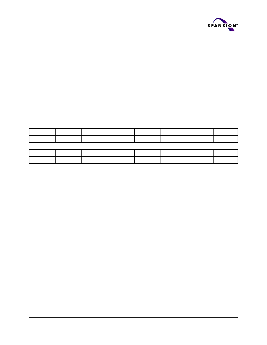
- Table 19. Memory Array Command Definitions (x32 Mode)
- Legend:
- Notes:
- 1. See Table 1 on page 14 for description of bus operations.
- 2. All values are in hexadecimal.
- 3. Shaded cells in table denote read cycles. All other cycles are write operations.
- 4. During unlock cycles, (lower address bits are 555 or 2AAh as shown in table) address bits higher than A11 (except where BA is required) and data bits higher than DQ7 are donêt cares.
- 5. No unlock or command cycles required when bank is reading array data.
- 6. The Reset command is required to return to the read mode (or to the erase-suspend-read mode if previously in Erase Suspend) when a bank is in the autoselect mode, or if DQ5 goes high (while the bank is providing status information).
- 7. The fourth cycle of the autoselect command sequence is a read cycle. The system must provide the bank address to obtain the manufacturer ID or device ID information. See the çAutoselect Commandé on page 44 section for more information.
- 8. This command cannot be executed until The Unlock Bypass command must be executed before writing this command sequence. The Unlock Bypass Reset command must be executed to return to normal operation.
- 9. This command is ignored during any embedded program, erase or suspended operation.
- 10. Valid read operations include asynchronous and burst read mode operations.
- 11. The device ID must be read across the fourth, fifth, and sixth cycles. 00h in the sixth cycle indicates ordering option 00, 01h indicates ordering option 01.
- 12. The system may read and program in non-erasing sectors, or enter the autoselect mode, when in the Program/Erase Suspend mode. The Program/Erase Suspend command is valid only during a sector erase operation, and requires the bank address.
- 13. The Program/Erase Resume command is valid only during the Erase Suspend mode, and requires the bank address.
- 14. Command is valid when device is ready to read array data or when device is in autoselect mode.
- 15. Asynchronous read operations.
- 16. ACC must be at VID during the entire operation of this command.
- 17. Command is ignored during any Embedded Program, Embedded Erase, or Suspend operation.
- 18. The Unlock Bypass Entry command is required prior to any Unlock Bypass operation. The Unlock Bypass Reset command is required to return to the read mode.
- Table 20. Sector Protection Command Definitions (x32 Mode)
- Write Operation Status
- DQ7: Data# Polling
- RY/BY#: Ready/Busy#
- DQ6: Toggle Bit I
- DQ2: Toggle Bit II
- Reading Toggle Bits DQ6/DQ2
- DQ5: Exceeded Timing Limits
- DQ3: Sector Erase Timer
- Absolute Maximum Ratings
- DC Characteristics
- Test Conditions
- Key to Switching Waveforms
- AC Characteristics
- Physical Dimensions
- Revision Summary

Publication Number S29CD016_00 Revision A Amendment 4 Issue Date November 5, 2004
The contents of this document are subject to change without notice. This document may contain information on a Spansion product under development by Spansion LLC. Spansion
LLC reserves the right to change or discontinue work on any product without notice. The information in this document is provided "as is" without warranty or guarantee of any
kind as to its accuracy, completeness, operability, fitness for particular purpose, merchantability, non-infringement of third-party rights, or any other warranty, express, implied, or
statutory. Spansion LLC assumes no liability for any damages of any kind arising out of the use of the information in this document.
S29CD016G
16 Megabit (512 K x 32-Bit)
CMOS 2.5 Volt-only Burst Mode, Dual Boot,
Simultaneous Read/Write Flash Memory
Data Sheet
Distinctive Characteristics
Architecture Advantages
Simultaneous Read/Write operations
-- Two bank architecture: large bank/ small bank
-- Data can be read from bank while executing erase/
program functions in other bank
-- Zero latency between read and write operations
User-Defined x32 Data Bus
Dual Boot Block
-- Top and bottom boot sectors in the same device
Flexible sector architecture
-- Eight 8 Kbytes, thirty 64 Kbytes, and eight 8 Kbytes
sectors
Manufactured on 170 nm process technology
SecSi (Secured Silicon) Sector (256 Bytes)
-- Factory locked and identifiable: 16 bytes for secure,
random factory Electronic Serial Number; remainder
may be customer data programmed by SpansionTM
-- Customer lockable: Can be read, programmed, or
erased just like other sectors. Once locked, data
cannot be changed
Programmable Burst interface
-- Interface to any high performance processor
-- Modes of Burst Read Operation:
-- Linear Burst: 4 double words and 8 double words
with wrap around
Program Operation
-- Ability to perform synchronous and asynchronous
write operations of burst configuration register
settings independently
Single power supply operation
-- Optimized for 2.5 to 2.75 volt read, erase, and
program operations
Compatibility with JEDEC standards (JC42.4)
-- Software compatible with single-power supply Flash
-- Backward-compatible with AMD Am29LV and Am29F
and Fujitsu MBM29LV and MBM29F flash memories
Performance Characteristics
High performance read access
-- Initial/random access times as fast as 54 ns
-- Burst access time as fast as 9 ns for ball grid array
package
Ultra low power consumption
-- Burst Mode Read: 90 mA @ 66 MHz max,
-- Program/Erase: 50 mA max
-- Standby mode: CMOS: 60 µA max
1 million write cycles per sector typical
20 year data retention typical
VersatileI/OTM control
-- Device generates data output voltages and tolerates
data input voltages as determined by the voltage on
the V
IO
pin
-- 1.65 V to 2.75 V compatible I/O signals
-- 3.6 V tolerant I/O signals
Software Features
Persistent Sector Protection
-- A command sector protection method to lock
combinations of individual sectors and sector groups
to prevent program or erase operations within that
sector (requires only V
CC
levels)
Password Sector Protection
-- A sophisticated sector protection method to lock
combinations of individual sectors and sector groups
to prevent program or erase operations within that
sector using a user-definable 64-bit password
Supports Common Flash Interface (CFI)
Unlock Bypass Program Command
-- Reduces overall programming time when issuing
multiple program command sequences
Data# Polling and toggle bits
-- Provides a software method of detecting program or
erase operation completion
Hardware Features
Program Suspend/Resume & Erase Suspend/
Resume
-- Suspends program or erase operations to allow
reading, programming, or erasing in same bank
Hardware Reset (RESET#), Ready/Busy# (RY/
BY#), and Write Protect (WP#) inputs
ACC input
-- Accelerates programming time for higher throughput
during system production
Package options
-- 80-pin PQFP
-- 80-ball Fortified BGA

2
S29CD016G
S29CD016_00_A4 November 5, 2004
A d v a n c e I n f o r m a t i o n
General Description
The S29CD016G is a 16 Megabit, 2.5 Volt-only single power supply burst mode
flash memory device. The device can be configured for 524,288 double words.
The device can also be programmed in standard EPROM programmers.
To eliminate bus contention, each device includes separate chip enable (CE#),
write enable (WE#), and output enable (OE#) controls. Additional control inputs
are required for synchronous burst operations: Load Burst Address Valid (ADV#),
and Clock (CLK).
Each device requires only a single 2.5 or 2.6 Volt power supply (2.5 V to 2.75
V) for both read and write functions. A 12.0-volt V
PP
is not required for program
or erase operations, although an acceleration pin is available if faster program-
ming performance is required.
The device is entirely command set compatible with the JEDEC single-power-
supply Flash standard. The software command set is compatible with the com-
mand sets of the 5 V Am29F and 3 V Am29LV Flash families. Commands are
written to the command register using standard microprocessor write timing.
Register contents serve as inputs to an internal state-machine that controls the
erase and programming circuitry. Write cycles also internally latch addresses and
data needed for the programming and erase operations. Reading data out of the
device is similar to reading from other Flash or EPROM devices.
The Unlock Bypass mode facilitates faster programming times by requiring only
two write cycles to program data instead of four.
The Simultaneous Read/Write architecture provides simultaneous operation
by dividing the memory space into two banks. The device can begin programming
or erasing in one bank, and then simultaneously read from the other bank, with
zero latency. This releases the system from waiting for the completion of program
or erase operations. See
"Simultaneous Read/Write Operations Overview and Re-
strictions" on page 14
.
The device provides a 256-byte SecSiTM (Secured Silicon) Sector with an one-
time-programmable (OTP) mechanism.
In addition, the device features several levels of sector protection, which can dis-
able both the program and erase operations in certain sectors or sector groups:
Persistent Sector Protection is a command sector protection method that re-
places the old 12 V controlled protection method; Password Sector Protection
is a highly sophisticated protection method that requires a password before
changes to certain sectors or sector groups are permitted; WP# Hardware Pro-
tection prevents program or erase in the two outermost 8 Kbytes sectors of the
larger bank.
The device defaults to the Persistent Sector Protection mode. The customer must
then choose if the Standard or Password Protection method is most desirable. The
WP# Hardware Protection feature is always available, independent of the other
protection method chosen.
The VersatileI/OTM (V
CCQ
) feature allows the output voltage generated on the
device to be determined based on the V
IO
level. This feature allows this device to
operate in the 1.8 V I/O environment, driving and receiving signals to and from
other 1.8 V devices on the same bus.
The host system can detect whether a program or erase operation is complete by
observing the RY/BY# pin, by reading the DQ7 (Data# Polling), or DQ6 (toggle)

November 5, 2004 S29CD016_00_A4
S29CD016G
3
A d v a n c e I n f o r m a t i o n
status bits. After a program or erase cycle is completed, the device is ready to
read array data or accept another command.
The sector erase architecture allows memory sectors to be erased and repro-
grammed without affecting the data contents of other sectors. The device is fully
erased when shipped from the factory.
Hardware data protection measures include a low V
CC
detector that automat-
ically inhibits write operations during power transitions. The password and
software sector protection feature disables both program and erase opera-
tions in any combination of sectors of memory. This can be achieved in-system
at V
CC
level.
The Program/Erase Suspend/Erase Resume feature enables the user to put
erase on hold for any period of time to read data from, or program data to, any
sector that is not selected for erasure. True background erase can thus be
achieved.
The hardware RESET# pin terminates any operation in progress and resets the
internal state machine to reading array data.
The device offers two power-saving features. When addresses are stable for a
specified amount of time, the device enters the automatic sleep mode. The
system can also place the device into the standby mode. Power consumption is
greatly reduced in both these modes.
Spansion Flash technology combines years of Flash memory manufacturing ex-
perience to produce the highest levels of quality, reliability and cost effectiveness.
The device electrically erases all bits within a sector simultaneously via
Fowler-Nordheim tunnelling. The data is programmed using hot electron
injection.

4
S29CD016G
S29CD016_00_A4 November 5, 2004
A d v a n c e I n f o r m a t i o n
Table of Contents
Product Selector Guide . . . . . . . . . . . . . . . . . . . . . .7
Block Diagram . . . . . . . . . . . . . . . . . . . . . . . . . . . . .8
Block Diagram of Simultaneous Read/Write
Circuit . . . . . . . . . . . . . . . . . . . . . . . . . . . . . . . . . . . .9
Connection Diagrams . . . . . . . . . . . . . . . . . . . . . . 10
Special Package Handling Instructions . . . . . . . 11
Pin Configuration . . . . . . . . . . . . . . . . . . . . . . . . . . 12
Logic Symbols . . . . . . . . . . . . . . . . . . . . . . . . . . . . . 13
Ordering Information . . . . . . . . . . . . . . . . . . . . . . . 14
Device Bus Operations . . . . . . . . . . . . . . . . . . . . . . 15
Table 1. Device Bus Operation . . . . . . . . . . . . . . . . . 15
VersatileI/OTM (V
IO
) Control .............................................................. 15
Requirements for Reading Array Data ........................................... 16
Simultaneous Read/Write
Operations Overview and Restrictions .......................................... 16
Overview ............................................................................................................................16
Restrictions ........................................................................................................................16
Table 2. Bank Assignment for Boot Bank
Sector Devices . . . . . . . . . . . . . . . . . . . . . . . . . . . . 17
Simultaneous Read/Write Operations With Zero Latency ..... 17
Table 3. Ordering Option 00 . . . . . . . . . . . . . . . . . . . 17
Table 4. Ordering Option 01 . . . . . . . . . . . . . . . . . . . 17
Writing Commands/Command Sequences ................................... 17
Accelerated Program and Erase Operations ..........................................................18
Autoselect Functions ......................................................................................................18
Automatic Sleep Mode (ASM) ...........................................................18
Standby Mode ...................................................................................................................18
RESET#: Hardware Reset Pin ............................................................ 19
Output Disable Mode ...........................................................................19
Autoselect Mode ................................................................................... 19
Table 5. S29CD016G Autoselect Codes (High Voltage Meth-
od) . . . . . . . . . . . . . . . . . . . . . . . . . . . . . . . . . . . . 20
Asynchronous Read Operation (Non-Burst) ...............................20
Figure 1. Asynchronous Read Operation . . . . . . . . . . 21
Synchronous (Burst) Read Operation ............................................. 21
Linear Burst Read Operations ........................................................... 21
Table 6. 32- Bit Linear and Burst Data Order . . . . . . . 22
CE# Control in Linear Mode ...................................................................................... 23
ADV# Control In Linear Mode .................................................................................. 23
RESET# Control in Linear Mode ............................................................................... 23
OE# Control in Linear Mode ..................................................................................... 23
IND/WAIT# Operation in Linear Mode ................................................................. 23
Table 7. Valid Configuration Register Bit Definition for IND/
WAIT# . . . . . . . . . . . . . . . . . . . . . . . . . . . . . . . . . . 23
Figure 2. End of Burst Indicator (IND/WAIT#) Timing for
Linear 4-Double-Word Burst Operation . . . . . . . . . . . 24
Burst Access Timing Control ......................................................................................24
Initial Burst Access Delay Control ............................................................................24
Table 8. Burst Initial Access Delay . . . . . . . . . . . . . . 24
Figure 3. Burst Access Timing . . . . . . . . . . . . . . . . . 25
Burst CLK Edge Data Delivery ................................................................................... 25
Burst Data Hold Control ............................................................................................. 25
Asserting RESET# During A Burst Access .............................................................. 25
Configuration Register ........................................................................ 25
Table 9. Configuration Register Definitions . . . . . . . . . 26
Table 10. Configuration Register After Device Reset . . 28
Initial Access Delay Configuration ..................................................28
Sector Protection . . . . . . . . . . . . . . . . . . . . . . . . . . 28
Sector and Sector Groups ...........................................................................................28
Persistent Sector Protection .......................................................................................28
Password Sector Protection ........................................................................................28
WP# Hardware Protection .........................................................................................28
Persistent Sector Protection ............................................................ 29
Persistent Protection Bit (PPB) ..................................................................................29
Persistent Protection Bit Lock (PPB Lock) .............................................................29
Dynamic Protection Bit (DYB) ...................................................................................29
Table 11. Sector Protection Schemes . . . . . . . . . . . . . 30
Persistent Sector Protection Mode Locking Bit ...........................31
Password Protection Mode .................................................................31
Password and Password Mode Locking Bit ...................................32
64-bit Password ............................................................................................................... 32
Write Protect (WP#) ..........................................................................33
SecSiTM (Secured Silicon) Sector Protection ..................................33
SecSi Sector Protection Bit ................................................................34
Persistent Protection Bit Lock ..........................................................34
Hardware Data Protection ................................................................34
Low V
CC
Write Inhibit .................................................................................................. 34
Write Pulse "Glitch" Protection ................................................................................ 34
Logical Inhibit ................................................................................................................... 35
Power-Up Write Inhibit ................................................................................................ 35
V
CC
and V
IO
Power-up And Power-down Sequencing ...................................... 35
Table 12. Sector Addresses for Ordering Option 00 . . . 35
Table 13. Sector Addresses for Ordering Option 01 . . . 37
Common Flash Memory Interface (CFI) . . . . . . . 39
Table 14. CFI Query Identification String . . . . . . . . . . 39
Table 15. CFI System Interface String . . . . . . . . . . . . 40
Table 16. Device Geometry Definition . . . . . . . . . . . . 41
Table 17. CFI Primary Vendor-Specific Extended Query 42
Command Definitions . . . . . . . . . . . . . . . . . . . . . . 44
Reading Array Data in Non-burst Mode ...................................... 44
Reading Array Data in Burst Mode ................................................ 44
Read/Reset Command .........................................................................45
Autoselect Command ..........................................................................45
Program Command Sequence ...........................................................45
Accelerated Program Command ..................................................... 46
Unlock Bypass Command Sequence .............................................. 46
Figure 4. Program Operation . . . . . . . . . . . . . . . . . . 47
Unlock Bypass Entry Command .................................................................................47
Unlock Bypass Program Command ..........................................................................48
Unlock Bypass Chip Erase Command ......................................................................48
Unlock Bypass CFI Command ....................................................................................48
Unlock Bypass Reset Command ................................................................................48
Chip Erase Command ......................................................................... 48
Sector Erase Command ..................................................................... 49
Figure 5. Erase Operation . . . . . . . . . . . . . . . . . . . . 50
Sector Erase and Program Suspend Command .......................... 50
Sector Erase and Program Suspend Operation Mechanics .......51
Table 18. Allowed Operations During Erase/Program Sus-
pend . . . . . . . . . . . . . . . . . . . . . . . . . . . . . . . . . . . 51
Sector Erase and Program Resume Command ............................52
Configuration Register Read Command ........................................52
Configuration Register Write Command ......................................52
Common Flash Interface (CFI) Command ....................................52
SecSi Sector Entry Command ............................................................53

November 5, 2004 S29CD016_00_A4
S29CD016G
5
A d v a n c e I n f o r m a t i o n
Password Program Command .......................................................... 54
Password Verify Command ............................................................... 54
Password Protection Mode Locking Bit Program Command . 55
Persistent Sector Protection Mode Locking Bit Program Com-
mand ......................................................................................................... 55
SecSi Sector Protection Bit Program Command ........................ 55
PPB Lock Bit Set Command .............................................................. 55
DYB Write Command ........................................................................ 56
Password Unlock Command ............................................................. 56
PPB Program Command ..................................................................... 56
All PPB Erase Command .................................................................... 57
DYB Write .............................................................................................. 57
PPB Lock Bit Set .................................................................................... 57
DYB Status .............................................................................................. 57
PPB Status ............................................................................................... 57
PPB Lock Bit Status .............................................................................. 57
Non-volatile Protection Bit Program And Erase Flow ............. 58
Table 19. Memory Array Command Definitions (x32 Mode)
59
Table 20. Sector Protection Command Definitions (x32
Mode) . . . . . . . . . . . . . . . . . . . . . . . . . . . . . . . . . . 60
Write Operation Status . . . . . . . . . . . . . . . . . . . . . 61
DQ7: Data# Polling ............................................................................... 61
Figure 6. Data# Polling Algorithm . . . . . . . . . . . . . . 62
RY/BY#: Ready/Busy# ......................................................................... 63
DQ6: Toggle Bit I .................................................................................. 63
DQ2: Toggle Bit II ................................................................................ 64
Reading Toggle Bits DQ6/DQ2 ........................................................64
Figure 7. Toggle Bit Algorithm . . . . . . . . . . . . . . . . . 65
DQ5: Exceeded Timing Limits .......................................................... 66
DQ3: Sector Erase Timer ..................................................................66
Table 21. Write Operation Status . . . . . . . . . . . . . . . 66
Absolute Maximum Ratings . . . . . . . . . . . . . . . . . .67
Figure 8. Maximum Negative Overshoot Waveform . . 67
Figure 9. Maximum Positive Overshoot Waveform . . . 67
Operating Ranges . . . . . . . . . . . . . . . . . . . . . . . . . .67
Industrial (I) Devices ...................................................................................................... 67
Extended (E) Devices .................................................................................................... 67
V
CC
Supply Voltages ...................................................................................................... 67
V
IO
Supply Voltages ....................................................................................................... 67
DC Characteristics . . . . . . . . . . . . . . . . . . . . . . . . .68
Table 22. CMOS Compatible . . . . . . . . . . . . . . . . . . . 68
Figure 10. I
CC1
Current vs. Time (Showing Active and Auto-
matic Sleep Currents) . . . . . . . . . . . . . . . . . . . . . . . 69
Figure 11. Typical I
CC1
vs. Frequency . . . . . . . . . . . . 69
Test Conditions . . . . . . . . . . . . . . . . . . . . . . . . . . . 70
Figure 12. Test Setup . . . . . . . . . . . . . . . . . . . . . . . 70
Table 23. Test Specifications . . . . . . . . . . . . . . . . . . . 70
Key to Switching Waveforms . . . . . . . . . . . . . . . . 70
Switching Waveforms . . . . . . . . . . . . . . . . . . . . . . 70
Figure 13. Input Waveforms and Measurement Levels 70
AC Characteristics . . . . . . . . . . . . . . . . . . . . . . . . .71
Figure 14. V
CC
and V
IO
Power-up Diagram. . . . . . . . . 71
Table 24. Asynchronous Read Operations . . . . . . . . . . 72
Figure 15. Conventional Read Operations Timings . . . 72
Table 25. Burst Mode Read . . . . . . . . . . . . . . . . . . . . 73
Figure 16. Burst Mode Read (x32 Mode) . . . . . . . . . . 74
Figure 17. Asynchronous Command Write Timing. . . . 75
Figure 18. Synchronous Command Write/Read Timing 75
Table 26. Hardware Reset (RESET#) . . . . . . . . . . . . . 76
Figure 19. RESET# Timings . . . . . . . . . . . . . . . . . . . 76
Figure 20. WP# Timing . . . . . . . . . . . . . . . . . . . . . . 77
Table 27. Erase/Program Operations . . . . . . . . . . . . . 78
Figure 21. Program Operation Timings . . . . . . . . . . . 79
Figure 22. Chip/Sector Erase Operation Timings. . . . . 80
Figure 23. Back-to-back Cycle Timings . . . . . . . . . . . 80
Figure 24. Data# Polling Timings
(During Embedded Algorithms) . . . . . . . . . . . . . . . . 81
Figure 25. Toggle Bit Timings
(During Embedded Algorithms) . . . . . . . . . . . . . . . . 81
Figure 26. DQ2 vs. DQ6 for Erase/Erase Suspend Operations
82
Figure 27. Synchronous Data Polling Timing/Toggle Bit Tim-
ings . . . . . . . . . . . . . . . . . . . . . . . . . . . . . . . . . . . 82
Figure 28. Sector Protect/Unprotect Timing Diagram . 83
Table 28. Alternate CE# Controlled Erase/Program Opera-
tions . . . . . . . . . . . . . . . . . . . . . . . . . . . . . . . . . . . 84
Figure 29. Alternate CE# Controlled Write Operation Tim-
ings . . . . . . . . . . . . . . . . . . . . . . . . . . . . . . . . . . . 85
Table 29. Erase and Programming Performance . . . . . 86
Table 30. PQFP and Fortified BGA Pin Capacitance . . . . 86
Physical Dimensions . . . . . . . . . . . . . . . . . . . . . . . 87
PRQ080≠80-Lead Plastic Quad Flat Package 87
LAA080≠80-ball Fortified Ball Grid Array (13 x 11
mm) 88
Revision Summary . . . . . . . . . . . . . . . . . . . . . . . . . 89
6
S29CD016G
S29CD016_00_A4 November 5, 2004
A d v a n c e I n f o r m a t i o n
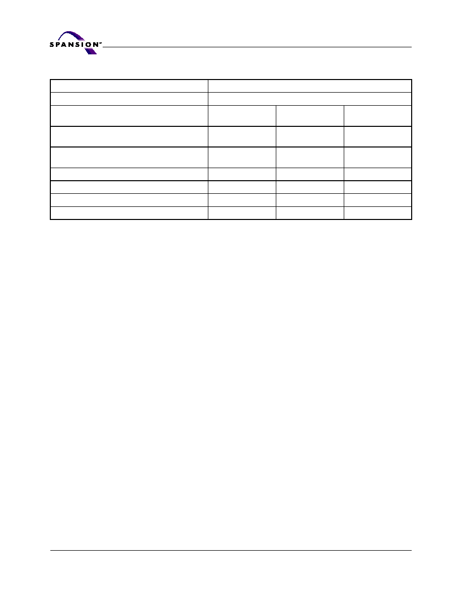
Product Selector Guide
Part Number
S29CD016G
Standard Voltage Range: V
CC
= 2.5 ≠ 2.75 V
Synchronous/Burst or Asynchronous
Speed Option (Clock Rate)
0P
(66 MHz)
0M
(56 MHz)
0J
(40 MHz)
Max Initial/Asynchronous
Access Time, ns (t
ACC
)
54
64
67
Max Burst Access Delay (ns)
9 FBGA/
9.5 PQFP
10 FBGA/
10 PQFP
17
Max Clock Rate (MHz)
66
56
40
Min Initial Clock Delay (clock cycles) See Figure 3
4
4
3
Max CE# Access, ns (t
CE
)
58
69
71
Max OE# Access, ns (t
OE
)
20
20
28

November 5, 2004 S29CD016_00_A4
S29CD016G
7
A d v a n c e I n f o r m a t i o n
Block Diagram
Input/Output
Buffers
X-Decoder
Y-Decoder
Chip Enable
Output Enable
Logic
Erase Voltage
Generator
PGM Voltage
Generator
Timer
VCC
Detector
State
Control
Command
Register
VCC
VSS
WE#
ACC
WP#
RESET#
CE#
OE#
DQ0≠DQ31
A0≠A18
Data
Latch
Y-Gating
Cell Matrix
Ad
d
r
e
s
s
La
t
c
h
DQ0≠DQ15
A0≠A18
Burst
State
Control
Burst
Address
Counter
ADV#
CLK
A0≠A18
VIO
IND/
WAIT#
RY/BY#
8
S29CD016G
S29CD016_00_A4 November 5, 2004
A d v a n c e I n f o r m a t i o n
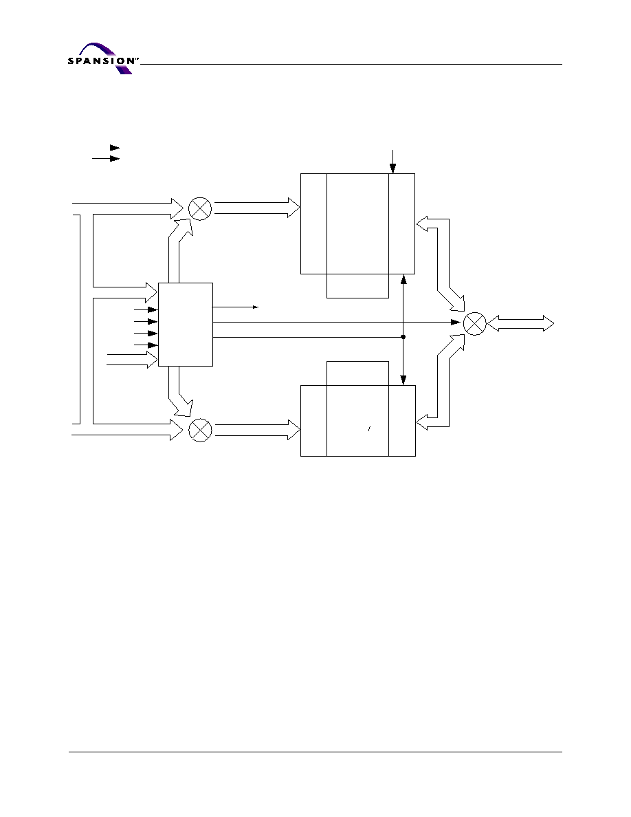
Block Diagram of Simultaneous Read/Write Circuit
V
CC
V
SS
Upper Bank Address
A0≠A18
RESET#
WE#
CE#
ADV#
DQ0≠DQ31
STATE
CONTROL
&
COMMAND
REGISTER
X-Decoder
Y-Decoder
Latches and Control Logic
OE#
DQ0≠DQ31
Lower Bank
(Bank 0)
Y-Decoder
X-Decoder
Latches and
Control Logic
Lower Bank Address
Status
Control
A0≠A18
A0≠A18
A0≠A18
A0≠A18
DQ0≠DQ31
DQ0≠DQ31
RY/BY#
Upper Bank
(Bank 1)
November 5, 2004 S29CD016_00_A4
S29CD016G
9
A d v a n c e I n f o r m a t i o n
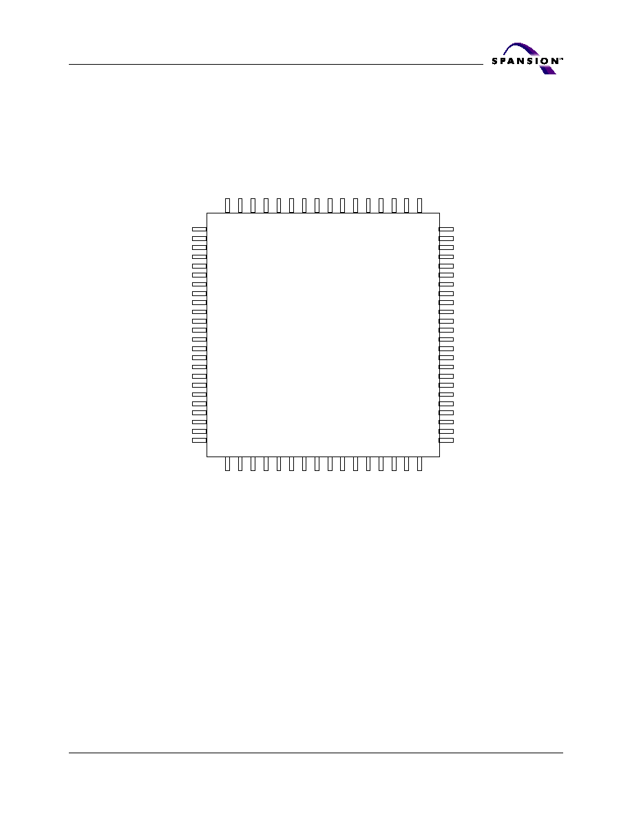
Connection Diagrams
1
2
3
4
5
6
7
8
9
10
11
12
13
14
15
16
17
18
19
20
21
22
23
24
DQ16
DQ17
DQ18
DQ19
V
CCQ
V
SS
DQ20
DQ21
DQ22
DQ23
DQ24
DQ25
DQ26
DQ27
V
CCQ
V
SS
DQ28
DQ29
DQ30
DQ31
MCH
A0
A1
A2
DQ15
DQ14
DQ13
DQ12
V
SS
V
CCQ
DQ11
DQ10
DQ9
DQ8
DQ7
DQ6
DQ5
DQ4
V
SS
V
CCQ
DQ3
DQ2
DQ1
DQ0
NC
A18
A17
A16
80 79 78 77 76 75 74 73 72 71 70 69 68 67 66 65
MCH
IND/W
AIT#
NC
WP#
WE#
OE#
CE#
V
CC
NC
V
SS
ADV#
R
Y/BY#
NC
CLK
RESET#
V
CCQ
A3
A4
A5
A6
A7
A8
V
SS
ACC
V
CC
A9
A10
A11
A12
A13
A14
A15
25
64
63
62
61
60
59
58
57
56
55
54
53
52
51
50
49
48
47
46
45
44
43
42
41
26 27 28 29 30 31 32 33 34 35 36 37 38 39 40
80-pin PQFP
Top View
10
S29CD016G
S29CD016_00_A4 November 5, 2004
A d v a n c e I n f o r m a t i o n
Connection Diagrams
Special Package Handling Instructions
Special handling is required for Flash Memory products in molded packages
(BGA). The package and/or data integrity may be compromised if the package
body is exposed to temperatures above 150∞C for prolonged periods of time.
B3
C3
D3
E3
F3
G3
H3
B4
C4
D4
E4
F4
G4
H4
B5
C5
D5
E5
F5
G5
H5
B6
C6
D6
E6
F6
G6
H6
B7
C7
D7
E7
F7
G7
H7
B8
C8
D8
E8
F8
G8
H8
DQ20
V
CCQ
V
SS
V
CCQ
DQ29
A0
A1
DQ18
DQ23
DQ24
DQ26
DQ30
MCH
A4
DQ19
DQ21
DQ25
DQ28
DQ31
A7
A5
DQ17
DQ22
RY/BY#
DQ27
NC
NC
A8
WP#
DQ9
DQ5
DQ1
NC
A10
A9
DQ11
DQ10
DQ6
DQ2
NC
A11
A12
A3
A4
A5
A6
A7
A8
A2
A3
A6
V
SS
ACC
V
CC
B2
C2
D2
E2
F2
G2
H2
DQ12
DQ8
DQ7
DQ4
DQ0
A18
A13
A2
A14
B1
C1
D1
E1
F1
G1
H1
DQ13
J3
J4
J5
J6
J7
J8
DQ16
IND/WAIT#
OE#
CE#
NC
ADV#
J2
DQ14
J1
DQ15
K3
K4
K5
K6
K7
K8
MCH
NC
WE#
V
CC
V
SS
CLK
K2
RESET#
K1
V
CCQ
V
CCQ
V
SS
V
CCQ
DQ3
A17
A16
A1
A15
80-Ball Fortified BGA
(Balls facing Down)

November 5, 2004 S29CD016_00_A4
S29CD016G
11
A d v a n c e I n f o r m a t i o n
Pin Configuration
A0≠A18
=
19-bit address bus for 16 Mb device. A9 supports 12
V autoselect inputs.
DQ0≠DQ31
=
32-bit data inputs/outputs/float
CE#
=
Chip Enable Input. This signal is asynchronous
relative to CLK for the burst mode.
OE#
=
Output Enable Input. This signal is asynchronous
relative to CLK for the burst mode.
WE#
=
Write enable. This signal is asynchronous relative to
CLK for the burst mode.
V
SS
= Device
ground
NC
=
Pin not connected internally
RY/BY#
=
Ready/Busy output and open drain. When RY/BY# =
V
IH
, the device is ready to accept read operations
and commands. When RY/BY# = V
OL
, the device is
either executing an embedded algorithm or the
device is executing a hardware reset operation (A
pull-up resistor is required.).
CLK
=
Clock Input that can be tied to the system or
microprocessor clock and provides the fundamental
timing and internal operating frequency.
ADV#
=
Load Burst Address input. Indicates that the valid
address is present on the address inputs.
IND/WAIT#
=
End of burst indicator for finite bursts only. IND/
WAIT# is low when the last word in the burst
sequence is at the data outputs. Otherwise the IND/
WAIT# is high when CE# is low.
WP#
=
Write Protect input. When WP# = V
OL
, the two
outermost bootblock sector in the 75% bank are
write protected regardless of other sector protection
configurations.
ACC
=
Acceleration input. When taken to 12 V, program and
erase operations are accelerated. When not used for
acceleration, ACC = V
SS
or V
CC
.
V
IO
(V
CCQ
)
=
Output Buffer Power Supply (1.65 V to 2.75 V, 3.6 V
tolerant)
V
CC
=
Chip Power Supply (2.5 V to 2.75 V)
RESET#
=
Hardware reset input
MCH
=
Must Connect High (to V
CC
)
12
S29CD016G
S29CD016_00_A4 November 5, 2004
A d v a n c e I n f o r m a t i o n
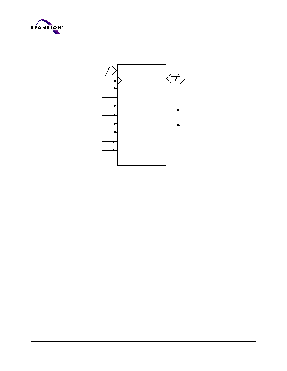
Logic Symbols
x32 Mode
19
32
DQ0≠DQ31
A0≠A18
CLK
RY/BY#
CE#
OE#
WE#
RESET#
ADV#
ACC
WP#
V
IO
(V
CCQ
)
IND/WAIT#
November 5, 2004 S29CD016_00_A4
S29CD016G
13
A d v a n c e I n f o r m a t i o n
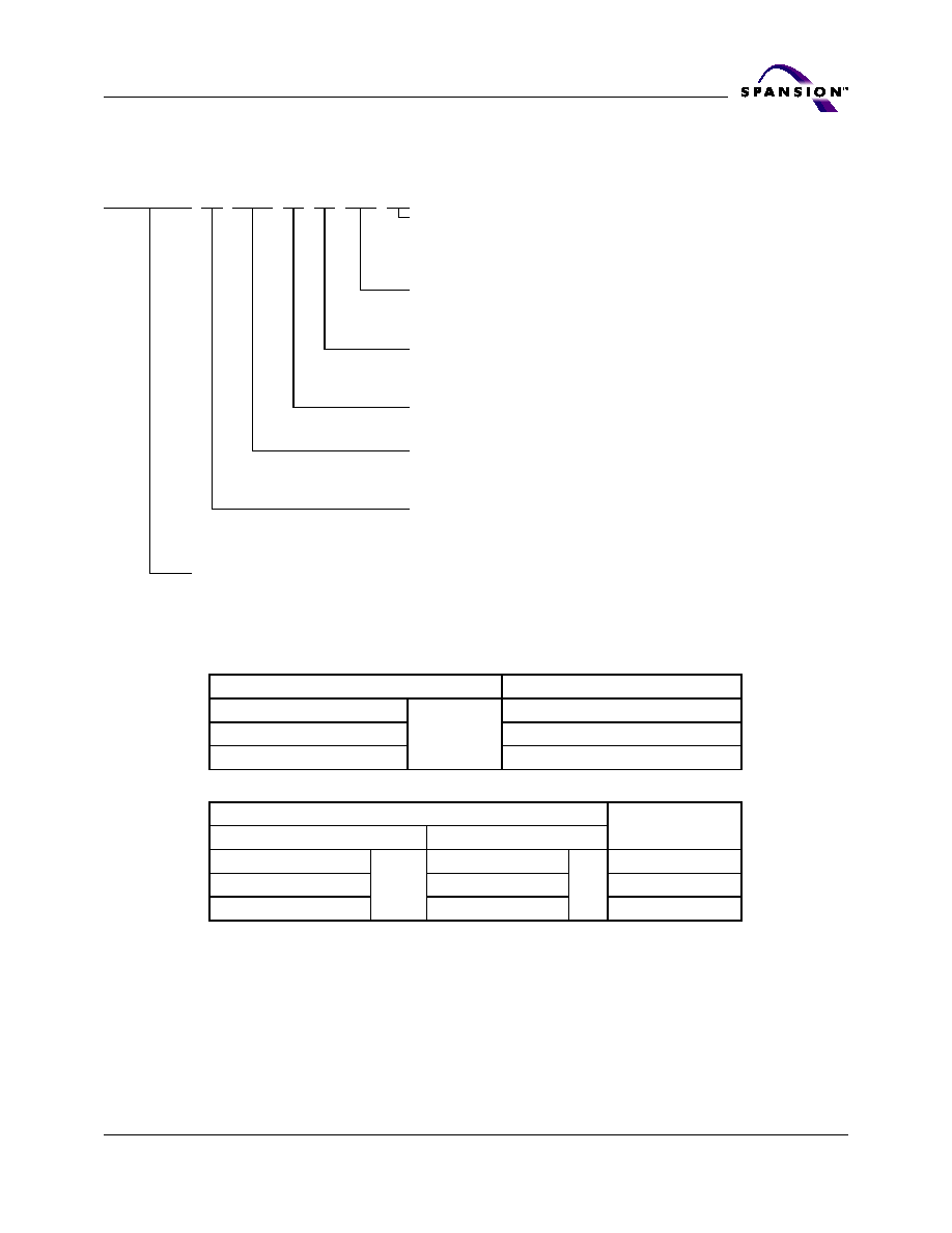
Ordering Information
The order number (Valid Combination) is formed by the following:
Valid Combinations
Valid Combinations list configurations planned to be supported in volume for this device.
Consult your local sales office to confirm availability of specific valid combinations and to
check on newly released combinations.
S29CD016G
0J
F
A
I
00
0
PACKING TYPE
0 =
Tray
2
= 7" Tape and Reel
3
= 13" Tape and Reel
ADDITIONAL ORDERING OPTIONS
00
= 4 Mb in Bank 0, 12 Mb in Bank 1, WP# protects sectors 44 and 45
01
= 12 Mb in Bank 0, 4 Mb in Bank 1, WP# protects sectors 0 and 1
TEMPERATURE RANGE
I =
Industrial
(≠40
∞
C to +85
∞
C)
N = Extended
(≠40
∞
C to +125
∞
C)
MATERIAL SET
A
= Standard
PACKAGE TYPE
Q
= Plastic Quad Flat Package (PQFP)
F
= Ball Fortified Ball Grid Array, 1.0 mm pitch package
CLOCK FREQUENCY
0J
= 40 MHz
0M
= 56 MHz
0P
= 66 MHz
DEVICE NUMBER/DESCRIPTION
S29CD016G
16 Megabit (512K x 32-Bit) CMOS 2.5 Volt-only Burst Mode,
Dual Boot, Simultaneous Read/Write Flash Memory
Manufactured on 170 nm floating gate technology
Valid Combinations for PQFP Packages
Clock Frequency
S29CD016G0P
QAI00
QAI01
QAN00
QAN01
66 MHz
S29CD016G0M
56 MHz
S29CD016G0J
40 MHz
Valid Combinations for Fortified BGA Packages
Clock Frequency
Order Number
Package Marking
S29CD016G0P
FAI00
FAI01
FAN00
FAN01
CD016G0PFA
I00
I01
N00
N01
66 MHz
S29CD016G0M
CD016G0MFA
56 MHz
S29CD016G0J
CD016G0JFA
40 MHz
14
S29CD016G
S29CD016_00_A4 November 5, 2004
A d v a n c e I n f o r m a t i o n
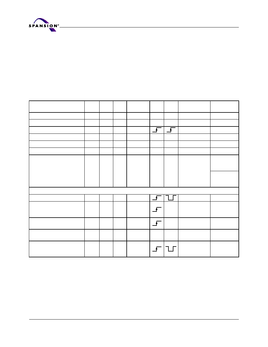
Device Bus Operations
This section describes the requirements and use of the device bus operations,
which are initiated through the internal command register. The command register
itself does not occupy any addressable memory location. The register is com-
posed of latches that store the commands, along with the address and data
information needed to execute the command. The contents of the register serve
as inputs to the internal state machine. The state machine outputs dictate the
function of the device.
Table 1
lists the device bus operations, the inputs and con-
trol levels they require, and the resulting output. The following subsections
describe each of these operations in further detail.
Legend:
L = Logic Low = V
IL
, H = Logic High = V
IH
, X = Don't care.
Notes:
1. WP# controls the two outermost sectors of the top boot block or the two outermost sectors of the bottom boot block.
2. DQ0 reflects the sector PPB (or sector group PPB) and DQ1 reflects the DYB.
VersatileI/OTM (V
IO
) Control
The VersatileI/O (V
IO
) control allows the host system to set the voltage levels that
the device generates at its data outputs and the voltages tolerated at its data in-
puts to the same voltage level that is asserted on the V
IO
pin.
Table 1. Device Bus Operation
Operation
CE#
OE#
WE#
RESET#
CLK
ADV#
Addresses
Data
(DQ0≠DQ31)
Read L
L
H
H
X
X
A
IN
D
OUT
Asynchronous Write
L
H
L
H
X
X
A
IN
D
IN
Synchronous Write
L
H
L
H
A
IN
D
IN
Standby (CE#)
H
X
X
H
X
X
X
HIGH Z
Output Disable
L
H
H
H
X
X
HIGH Z
HIGH Z
Reset
X
X
X
L
X
X
X
HIGH Z
PPB Protection Status (Note 2)
L
L
H
H
X
X
Sector Address,
A9 = V
ID
,
A7 ≠ A0 = 02h
00000001h,
(protected)
A6 = H
00000000h
(unprotect)
A6 = L
Burst Read Operations
Load Starting Burst Address
L
X
H
H
A
IN
X
Advance Burst to next address
with appropriate Data
presented on the Data bus
L
L
H
H
H
X
Burst Data Out
Terminate Current Burst Read
Cycle
H
X
H
H
X
X
HIGH Z
Terminate Current Burst Read
Cycle with RESET#
X
X
H
L
X
X
X
HIGH Z
Terminate Current Burst Read
Cycle; Start New Burst Read
Cycle
L
H
H
H
A
IN
X

November 5, 2004 S29CD016_00_A4
S29CD016G
15
A d v a n c e I n f o r m a t i o n
The output voltage generated on the device is determined based on the V
IO
(V
CCQ
) level.
A V
IO
of 1.65≠1.95 volts is targeted to provide for I/O tolerance at the 1.8 volt
level.
A V
CC
and V
IO
of 2.5≠2.75 volts makes the device appear as 2.5 volt-only.
Requirements for Reading Array Data
To read array data from the outputs, the system must drive the CE# and OE#
pins to V
IL
. CE# is the power control and selects the device. OE# is the output
control and gates array data to the output pins. WE# should remain at V
IH
.
The internal state machine is set for reading array data upon device power-up,
or after a hardware reset. This ensures that no spurious alteration of the memory
content occurs during the power transition. No command is necessary in this
mode to obtain array data. Standard microprocessor read cycles that assert valid
addresses on the device address inputs produce valid data on the device data
outputs. The device remains enabled for read access until the command register
contents are altered.
Address access time (t
ACC
) is the delay from stable addresses to valid output
data. The chip enable access time (t
CE
) is the delay from stable addresses and
stable CE# to valid data at the output pins. The output enable access time (t
OE
)
is the delay from the falling edge of OE# to valid data at the output pins (assum-
ing the addresses are stable for at least t
ACC
≠t
OE
time and CE# is asserted for at
least t
CE
≠t
OE
time).
See "
"Reading Array Data in Non-burst Mode" on page 42
" for more information.
Refer to the AC Read Operations table for timing specifications and to
Table 1 on
page 20
for the timing diagram. I
CC1
in the DC Characteristics table represents
the active current specification for reading array data.
Simultaneous Read/Write
Operations Overview and Restrictions
Overview
The Simultaneous Read/Write feature allows a program or erase operation to be
executed in one (busy) bank, while performing other operations in the other bank
(non-busy).
The Simultaneous Read/Write operation of this device was optimized for applica-
tions that could most benefit from this capability. These applications store code
in the larger bank, while storing data in the smaller bank. The best example of
this is when a Sector Erase Operation (as an embedded operation) in the smaller
(busy) bank occurs, while performing a Burst/synchronous Read Operation in the
larger (non-busy) bank.
Restrictions
The Simultaneous Read/Write function is tested by executing an embedded op-
eration in the small (busy) bank while performing other operations in the big
(non-busy) bank. However, the opposite case is neither tested nor valid. That is,
it is not tested by executing an embedded operation in the big (busy) bank while
performing other operations in the small (non-busy) bank. See the following ta-
bles,
Table 2 on page 16
,
Table 18 on page 50
,
Table 12 on page 34
, and
Table 13
on page 36
16
S29CD016G
S29CD016_00_A4 November 5, 2004
A d v a n c e I n f o r m a t i o n
Table 2. Bank Assignment for Boot Bank
Sector Devices
Simultaneous Read/Write Operations With Zero Latency
The device is capable of reading data from one bank of memory while program-
ming or erasing in the other bank of memory. An erase operation may also be
suspended to read from or program to another location within the same bank (ex-
cept the sector being erased). Refer to the table in
"DC Characteristics" on
page 67
for read-while-program and read-while-erase current specifications.
Simultaneous read/write operations are valid for both the main Flash memory
array and the SecSi OTP sector. Simultaneous Read/Write is disabled during the
CFI and Password Program/Verify operations. PPB Program/Erase operations and
the Password Unlock operation permit reading data from the large (75%) bank
while reading the operation status of these commands from the small (25%)
bank.
Table 3. Ordering Option 00
Table 4. Ordering Option 01
Writing Commands/Command Sequences
To write a command or command sequence (which includes programming data
to the device and erasing sectors of memory), the system must drive WE# and
CE# to V
IL
, and OE# to V
IH
.
The device features an Unlock Bypass mode to facilitate faster programming.
Once the device enters the Unlock Bypass mode, only two write cycles are re-
quired to program a word or byte, instead of four. The
"Sector Erase and Program
Suspend Command" on page 49
contains details on programming data to the de-
vice using both standard and Unlock Bypass command sequences.
An erase operation can erase one sector, multiple sectors, or the entire device.
Table 12 on page 34
and
Table 13 on page 36
indicate the address space that
each sector occupies. A "sector address" consists of the address bits required to
uniquely select a sector. The
"Command Definitions" on page 43
contain details
regarding erasing a sector or the entire chip, or suspending/resuming the erase
operation.
After the system writes the autoselect command sequence, the device enters the
autoselect mode. The system can then read autoselect codes from the internal
register (which is separate from the memory array) on DQ7≠DQ0. Standard read
Bank
Ordering Option 00
Ordering Option 01
Bank 0
Small Bank
Big Bank
Bank 1
Big Bank
Small Bank
Bank
A18:A17
Bank 0
00
Bank 1
01, 1X
Bank
A18:A17
Bank 0
0X, 10
Bank 1
11

November 5, 2004 S29CD016_00_A4
S29CD016G
17
A d v a n c e I n f o r m a t i o n
cycle timing applies in this mode. Refer to
"Autoselect Mode" on page 18
for more
information.
I
CC2
and I
CC3
in the DC Characteristics table represents the active current speci-
fication for erase or program modes. The
"AC Characteristics" on page 70
section
contains timing specification tables and timing diagrams for erase or program
operations.
When in Synchronous read mode configuration, the device is able to perform both
asynchronous and synchronous write operations. CLK and ADV# address latch is
supported in synchronous programming mode. During a synchronous write oper-
ation, to write a command or command sequence, (which includes programming
data to the device and erasing sectors of memory), the system must drive ADV#
and CE# to VIL, and OE# to VIH when providing an address to the device, and
drive WE# and CE# to VIL, and CE# to VIH, when writing commands or data.
Accelerated Program and Erase Operations
The device offers accelerated program/erase operations through the ACC pin.
When the system asserts V
HH
(12V) on the ACC pin, the device automatically en-
ters the Unlock Bypass mode. The system may then write the two-cycle Unlock
Bypass program command sequence to do accelerated programming. The device
uses the higher voltage on the ACC pin to accelerate the operation. A sector that
is being protected with the WP# pin is still protected during accelerated program
or Erase. Note that the ACC pin must not be at V
HH
during any operation other
than accelerated programming, or device damage may result. When accelerated
program/erase is not in use, set ACC=V
ss
or ACC=V
cc
.
Autoselect Functions
If the system writes the autoselect command sequence, the device enters the au-
toselect mode. The system can then read autoselect codes from the internal
register (which is separate from the memory array) on DQ7≠DQ0. Standard read
cycle timings apply in this mode. Refer to the
"Autoselect Mode" on page 18
and
"Autoselect Command" on page 44
sections for more information.
Automatic Sleep Mode (ASM)
The automatic sleep mode minimizes Flash device energy consumption. While in
asynchronous mode, the device automatically enables this mode when addresses
remain stable for t
ACC
+ 60 ns. The automatic sleep mode is independent of the
CE#, WE# and OE# control signals. Standard address access timings provide
new data when addresses are changed. While in sleep mode, output data is
latched and always available to the system. While in synchronous mode, the de-
vice automatically enables this mode when either the first active CLK level is
greater than t
ACC
or the CLK runs slower than 5 MHz. Note that a new burst op-
eration is required to provide new data.
I
CC8
in the "DC Characteristics" section represents the automatic sleep mode cur-
rent specification.
Standby Mode
When the system is not responding or writing to the device, it can place the de-
vice in the standby mode. In this mode, current consumption is greatly reduced,
and the outputs are placed in the high impedance state, independent of the OE#
input.

18
S29CD016G
S29CD016_00_A4 November 5, 2004
A d v a n c e I n f o r m a t i o n
The device enters the CMOS standby mode when the CE# and RESET# inputs are
both held at Vcc ± 0.2 V. The device requires standard access time (t
CE
) for read
access, before it is ready to read data.
If the device is deselected during erasure or programming, the device draws ac-
tive current until the operation is completed.
I
CC5
in the "DC Characteristics" section represents the standby current
specification.
Caution: Entering the standby mode via the RESET# pin also resets the device
to the read mode and floats the data I/O pins. Furthermore, entering I
CC7
during
a program or erase operation l leaves erroneous data in the address locations
being operated on at the time of the RESET# pulse. These locations require up-
dating after the device resumes standard operations. Refer to
""RESET#:
Hardware Reset Pin" on page 18
for further discussion of the RESET# pin and its
functions.
RESET#: Hardware Reset Pin
The RESET# pin is an active low signal that is used to reset the device under any
circumstances. A logic "0" on this pin forces the device out of any mode that is
currently executing back to the reset state. The RESET# pin may be tied to the
system reset circuitry. A system reset would thus also reset the device. To avoid
a potential bus contention during a system reset, the device is isolated from the
DQ data bus by tristating the data output pins for the duration of the RESET
pulse. All pins are "don't care" during the reset operation.
If RESET# is asserted during a program or erase operation, the RY/BY# pin re-
mains low until the reset operation is internally complete. This action requires
between 1 µs and 7µs for either Chip Erase or Sector Erase. The RY/BY# pin can
be used to determine when the reset operation is complete. Otherwise, allow for
the maximum reset time of 11 µs. If RESET# is asserted when a program or erase
operation is not executing (RY/BY# = "1"), the reset operation completes within
500 ns. The Simultaneous Read/Write feature of this device allows the user to
read a bank after 500 ns if the bank was in the read/reset mode at the time RE-
SET# was asserted. If one of the banks was in the middle of either a program or
erase operation when RESET# was asserted, the user must wait 11 µs before ac-
cessing that bank.
Asserting RESET# during a program or erase operation leaves erroneous data
stored in the address locations being operated on at the time of device reset.
These locations need updating after the reset operation is complete. See
Figure 19, on page 75
for timing specifications.
Asserting RESET# active during V
CC
and V
IO
power-up is required to guarantee
proper device initialization until V
CC
and V
IO
have reached their steady state
voltages.
Output Disable Mode
See
Table 1 on page 14
for OE# Operation in Output Disable Mode.
Autoselect Mode
The autoselect mode provides manufacturer and device identification, and sector
protection verification, through identifier codes output on DQ7≠DQ0. This mode
is primarily intended for programming equipment to automatically match a device

November 5, 2004 S29CD016_00_A4
S29CD016G
19
A d v a n c e I n f o r m a t i o n
to be programmed with its corresponding programming algorithm. However, the
autoselect codes can also be accessed in-system through the command register.
When using programming equipment, the autoselect mode requires V
ID
on ad-
dress pin A9. Address pins A6, A1, and A0 must be as shown in
Table 12 on
page 34
(top boot devices) or
Table 13 on page 36
(bottom boot devices). In ad-
dition, when verifying sector protection, the sector address must appear on the
appropriate highest order address bits (see Tables 1 and).
Table 5
shows the re-
maining address bits that are don't care. When all necessary bits are set as
required, the programming equipment may then read the corresponding identi-
fier code on DQ7≠DQ0.
To access the autoselect codes in-system, the host system can issue the autose-
lect command via the command. This method does not require V
ID
. See
"Command Definitions" on page 43
for details on using the autoselect mode.
Table 5. S29CD016G Autoselect Codes (High Voltage Method)
L = Logic Low = V
IL
, H = Logic High = V
IH
, SA = Sector Address, X = Don't care.
Note: The autoselect codes may also be accessed in-system via command sequences. See Tables 18 and 20.
Asynchronous Read Operation (Non-Burst)
The device includes two control functions which must be satisfied in order to ob-
tain data at the outputs. CE# is the power control and should be used for device
selection. OE# is the output control and should be used to gate data to the output
pins if the device is selected. The device is power-up in an asynchronous read
mode. In the asynchronous mode the device includes two control functions which
must be satisfied in order to obtain data at the outputs. CE# is the power control
and should be used for device selection. OE# is the output control and should be
used to gate data to the output pins if the device is selected.
Address access time (t
ACC
) is equal to the delay from stable addresses to valid
output data. The chip enable access time (t
CE
) is the delay from the stable ad-
dresses and stable CE# to valid data at the output pins. The output enable access
time is the delay from the falling edge of OE# to valid data at the output pins
(assuming the addresses are stable for at least t
ACC
≠t
OE
time).
Description
CE# OE# WE#
A18
to
A11
A10
A9
A8
A7
A6
A5
to
A4
A3
A2
A1
A0
DQ7
to
DQ0
Manufacturer ID:
Spansion
L
L
H
X
X
V
ID
X
X
L
X
L
L
L
L
0001h
A
u
tosel
e
ct
De
vi
ce C
o
d
e
Read Cycle 1
L
L
H
X
X
V
ID
X
L
L
X
L
L
L
H
007Eh
Read Cycle 2
L
L
H
X
X
V
ID
X
L
L
L
H
H
H
L
0036h
Read Cycle 3
L
L
H
X
X
V
ID
X
L
L
L
H
H
H
H
0000h
Ordering Option
00
0001h
Ordering Option
01
PPB Protection
Status
L
L
H
SA
X
V
ID
X
L
L
L
L
L
H
L
0000h
(unprotected)
0001h
(protected)
20
S29CD016G
S29CD016_00_A4 November 5, 2004
A d v a n c e I n f o r m a t i o n
Note: Operation is shown for the 32-bit data bus.
Figure 1. Asynchronous Read Operation
Synchronous (Burst) Read Operation
The device is capable of performing burst read operations to improve total system
data throughput. The 2, 4, and 8 double word accesses are configurable as linear
burst accesses. All burst operations provide wrap around linear burst accesses.
Additional options for all burst modes include initial access delay configurations
(2≠16 CLKs) Device configuration for burst mode operation is accomplished by
writing the Configuration Register with the desired burst configuration informa-
tion. Once the Configuration Register is written to enable burst mode operation,
all subsequent reads from the array are returned using the burst mode protocols.
Like the main memory access, the SecSi Sector memory is accessed with the
same burst or asynchronous timing as defined in the Configuration Register. How-
ever, the user must recognize burst operations past the 256 byte SecSi boundary
returns invalid data.
Burst read operations occur only to the main flash memory arrays. The Configu-
ration Register and protection bits are treated as single cycle reads, even when
burst mode is enabled. Read operations to these locations results in the data re-
maining valid while OE# is at V
IL
, regardless of the number of CLK cycles applied
to the device.
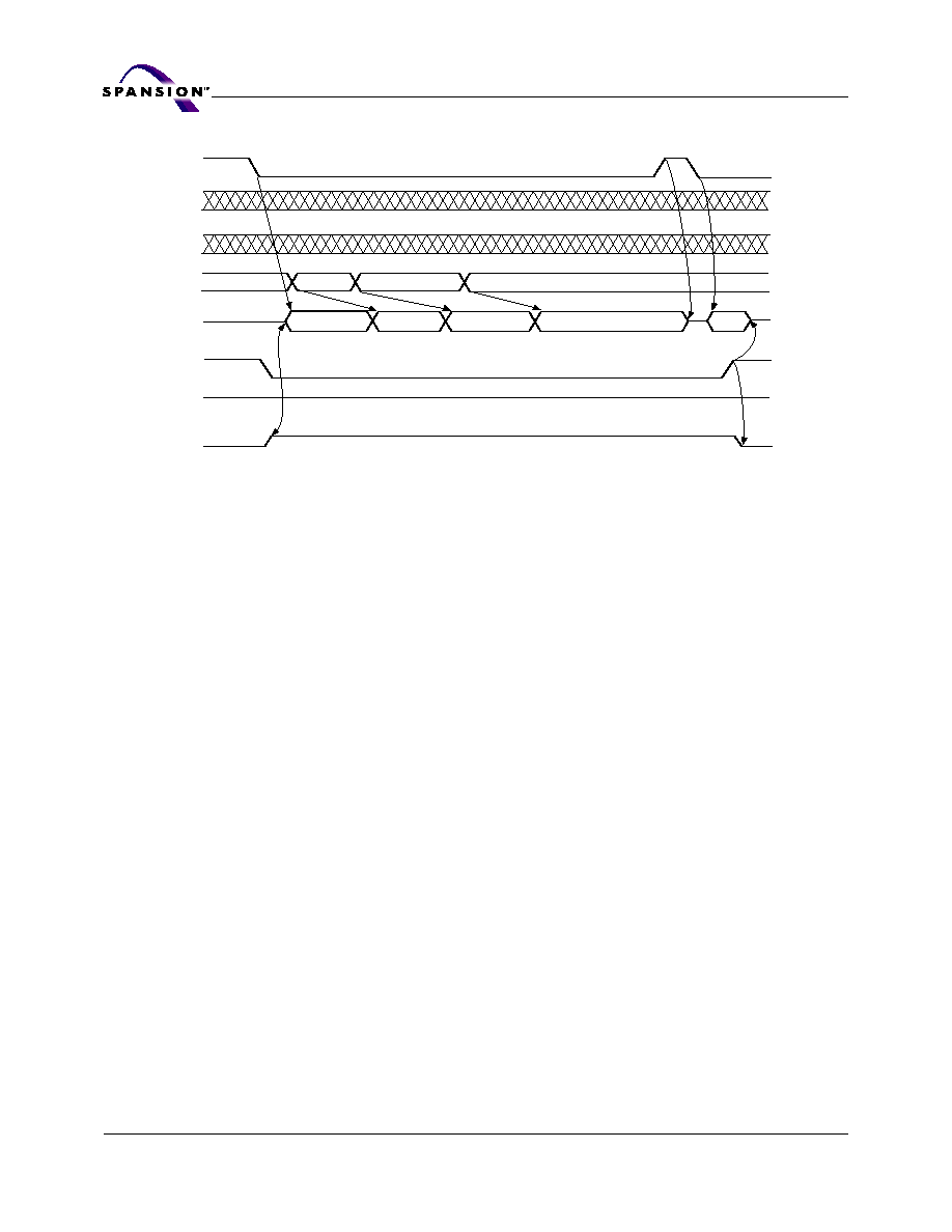
Linear Burst Read Operations
Linear burst read mode reads either 2, 4, or 8 double words (1 double word = 32
bits). (See
Table 6 on page 21
for all valid burst output sequences). The IND/
WAIT# pin transitions active (V
IL
) during the last transfer of data during a linear
burst read before a wrap around, indicating that the system should initiate an-
other ADV# to start the next burst access. If the system continues to clock the
device, the next access wraps around to the starting address of the previous
burst access. The IND/WAIT# signal remains inactive (floating) when not active.
See
Table 6 on page 21
for a complete 32-bit data bus interface order.
D0
D1 D2
D3
D3
CE#
CLK
ADV#
Addresses
Data
OE#
WE#
IND/WAIT#
V
IH
Float
V
OH
Address 0
Address 1
Address 2
Address 3
Float
November 5, 2004 S29CD016_00_A4
S29CD016G
21
A d v a n c e I n f o r m a t i o n
Table 6. 32- Bit Linear and Burst Data Order
Data Transfer Sequence
(Independent of the WORD# pin)
Output Data Sequence (Initial Access Address)
Two Linear Data Transfers
0-1 (A0 = 0)
1-0 (A0 = 1)
Four Linear Data Transfers
0-1-2-3 (A1-A0 = 00)
1-2-3-0 (A1-A0 = 01)
2-3-0-1 (A1-A0 = 10)
3-0-1-2 (A1-A0 = 11)
Eight Linear Data Transfers
0-1-2-3-4-5-6-7 (A2-A0 = 000)
1-2-3-4-5-6-7-0 (A2-A0 = 001)
2-3-4-5-6-7-0-1 (A2-A0 = 010)
3-4-5-6-7-0-1-2 (A2-A0 = 011)
4-5-6-7-0-1-2-3 (A2-A0 = 100)
5-6-7-0-1-2-3-4 (A2-A0 = 101)
6-7-0-1-2-3-4-5 (A2-A0 = 110)
7-0-1-2-3-4-5-6 (A2-A0 = 111)

22
S29CD016G
S29CD016_00_A4 November 5, 2004
A d v a n c e I n f o r m a t i o n
CE# Control in Linear Mode
The CE# (Chip Enable) pin enables the device during read mode operations. CE#
must meet the required burst read setup times for burst cycle initiation. If CE#
is taken to V
IH
at any time during the burst linear or burst cycle, the device im-
mediately exits the burst sequence and floats the DQ bus and IND/WAIT# signal.
Restarting a burst cycle is accomplished by taking CE# and ADV# to V
IL
.
ADV# Control In Linear Mode
The ADV# (Address Valid) pin is used to initiate a linear burst cycle at the clock
edge when CE# and ADV# are at V
IL
and the device is configured for either linear
burst mode operation. A burst access is initiated and the address is latched on
the first rising CLK edge when ADV# is active or upon a rising ADV# edge, which-
ever occurs first. If the ADV# signal is taken to V
IL
prior to the end of a linear
burst sequence, the previous address is discarded and subsequent burst transfers
are invalid until ADV# transitions to V
IH
before a clock edge, which initiates a new
burst sequence.
RESET# Control in Linear Mode
The RESET# pin immediately halts the linear burst access when taken to V
IL
. The
DQ data bus and IND/WAIT# signal float. Additionally, the Configuration Register
contents are reset back to the default condition where the device is placed in
asynchronous access mode.
OE# Control in Linear Mode
The OE# (Output Enable) pin is used to enable the linear burst data on the DQ
data bus and the IND/WAIT# pin. De-asserting the OE# pin to V
IH
during a burst
operation floats the data bus and the IND/WAIT# pin. However, the device con-
tinues to operate internally as if the burst sequence continues until the linear
burst is complete. The OE# pin does not halt the burst sequence, this is accom-
plished by either taking CE# to V
IH
or re-issuing a new ADV# pulse. The DQ bus
and IND/WAIT# signal remain in the float state until OE# is taken to V
IL
.
IND/WAIT# Operation in Linear Mode
The IND/WAIT#, or End of Burst Indicator signal (when in linear modes), informs
the system that the last address of a burst sequence is on the DQ data bus. For
example, with a 2-double-word linear burst, the IND/WAIT# signal transitions ac-
tive on the second access. If the same scenario is used, the IND/WAIT# signal
has the same delay and setup timing as the DQ pins. Also, the IND/WAIT# signal
is controlled by the OE# signal. If OE# is at V
IH
, the IND/WAIT# signal floats and
is not driven. If OE# is at V
IL
, the IND/WAIT# signal is driven at V
IH
until it tran-
sitions to V
IL
indicating the end of burst sequence. The IND/WAIT# signal timing
and duration is (See
"Configuration Register" on page 24
for more information).
Table 7
lists the valid combinations of the Configuration Register bits that impact
the IND/WAIT# timing.
Table 7. Valid Configuration Register Bit Definition for IND/WAIT#
DOC
WC
CC
Definition
0
0
1
IND/WAIT# = VIL for 1-CLK cycle, Active on last transfer, Driven on rising CLD edge
0
1
1
IND/WAIT# = VIL for 1-CLK cycle, Active on second to last transfer, Driven on rising CLK edge
November 5, 2004 S29CD016_00_A4
S29CD016G
23
A d v a n c e I n f o r m a t i o n
Burst Access Timing Control
In addition to the IND/WAIT# signal control, burst controls exist in the Control
Register for initial access delay, delivery of data on the CLK edge, and the length
of time data is held.
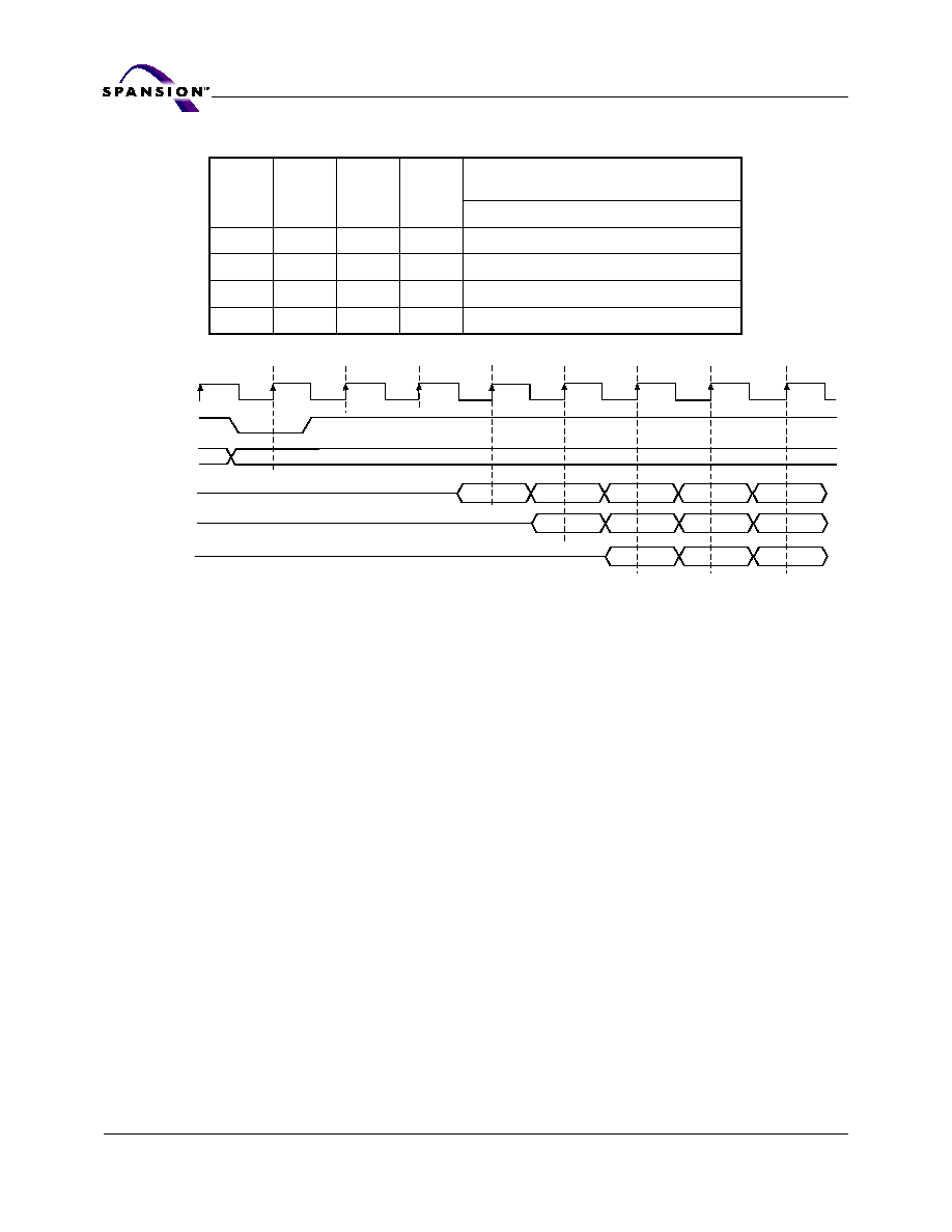
Initial Burst Access Delay Control
The device contains options for initial access delay of a burst access. The initial
access delay has no effect on asynchronous read operations.
Burst Initial Access Delay is defined as the number of clock cycles that must
elapse from the first valid clock edge after ADV# assertion (or the rising edge of
ADV#) until the first valid CLK edge when the data is valid.
The burst access is initiated and the address is latched on the first rising CLK edge
when ADV# is active or upon a rising ADV# edge, whichever comes first. (
Table
8
shows the initial access delay configurations.)
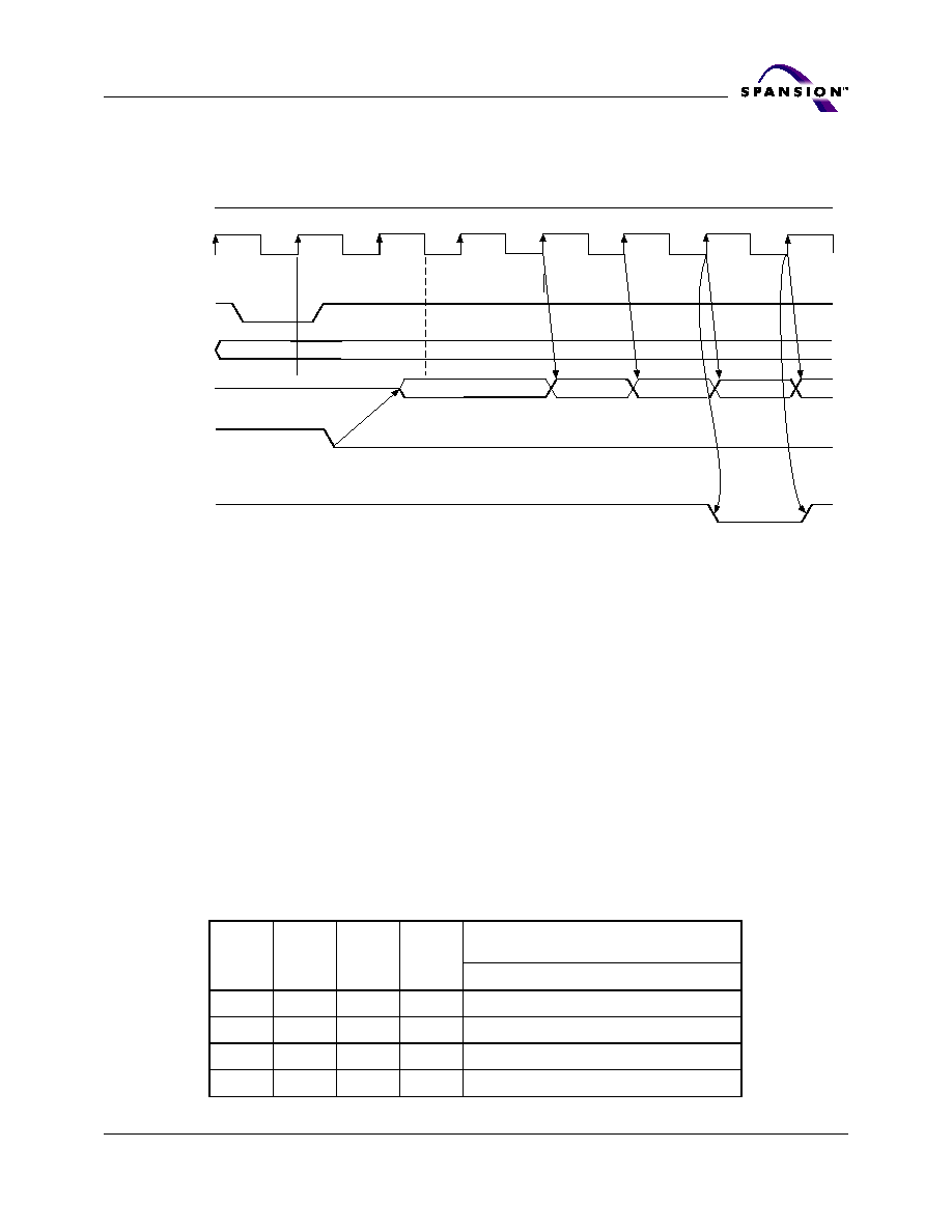
Figure 2. End of Burst Indicator (IND/WAIT#) Timing for Linear 4-Double-Word Burst Operation
Table 8. Burst Initial Access Delay (Sheet 1 of 2)
CR13
CR12
CR11
CR10
Initial Burst Access
(CLK cycles)
0
0
0
0
2
0
0
0
1
3
0
0
1
0
4
0
0
1
1
5
CE#
CLK
ADV#
Addresses
OE#
Data
Address 1
Invalid
D1
D2
D3
D0
Address 1 Latched
3 Clock Delay
IND/WAIT#
V
IL
V
IH
Note: Operation is shown for the 32-bit data bus. Figure shown with 3-CLK initial access
delay configuration, linear address, 4-double-word burst, output on rising CLK edge, data hold for 1-CLK, IND/
WAIT# asserted on the last transfer before wrap-around
24
S29CD016G
S29CD016_00_A4 November 5, 2004
A d v a n c e I n f o r m a t i o n
Figure 3. Burst Access Timing
Notes:
1. Burst access starts with a rising CLK edge and when ADV# is active.
2. Configurations register 6 must be always set to 1 (CR6 = 1). Burst starts and data outputs on the rising CLK edge.
3. CR [13-10] = 0001 or three clock cycles
4. CR [13-10] = 0010 or four clock cycles
5. CR [13-10] = 0011 or five clock cycles
Burst CLK Edge Data Delivery
The device is capable of delivering data on either the rising or falling edge of CLK.
To deliver data on the rising edge of CLK, bit 6 in the Control Register (CR6) is
set to 1. The default configuration is set to the rising edge.
Burst Data Hold Control
The device is capable of holding data for one CLKs. The default configuration is
to hold data for one CLK and is the only valid state.
Asserting RESET# During A Burst Access
If RESET# is asserted low during a burst access, the burst access is immediately
terminated and the device defaults back to asynchronous read mode. Refer to
"RESET#: Hardware Reset Pin" on page 18
for more information on the RESET#
function.
Configuration Register
The device contains a Configuration Register for configuring read accesses. The
Configuration Register is accessed by the Configuration Register Read and the
Configuration Register Write commands. The Configuration Register does not oc-
0
1
0
0
6
0
1
0
1
7
0 1
1
0
8
0
1
1
1
9
Table 8. Burst Initial Access Delay (Sheet 2 of 2)
CR13
CR12
CR11
CR10
Initial Burst Access
(CLK cycles)
CLK
ADV#
Addresses
DQ31-DQ0
3
DQ31-DQ0
4
DQ31-DQ0
5
Valid Address
Three CLK Delay
2nd CLK
3rd CLK
4th CLK
5th CLK
1st CLK
Four CLK Delay
Address 1 Latched
Five CLK Delay
D0
D1
D2
D3
D0
D1
D2
D0
D1
D2
D3
D4
November 5, 2004 S29CD016_00_A4
S29CD016G
25
A d v a n c e I n f o r m a t i o n
cupy any addressable memory location, but rather, is accessed by the
Configuration Register commands. The Configuration Register is readable any
time, however, writing the Configuration Register is restricted to times when the
Embedded AlgorithmTM is not active. If the user attempts to write the Configura-
tion Register while the Embedded AlgorithmTM is active, the write operation is
ignored and the contents of the Configuration Register remain unchanged.
The Configuration Register is a 16 bit data field which is accessed by DQ15≠DQ0.
During a read operation, DQ31≠DQ16 returns all zeroes.
Table 9
shows the Con-
figuration Register. Also, Configuration Register reads operate the same as
Autoselect command reads. When the command is issued, the bank address is
latched along with the command. Reads operations to the bank that was specified
during the Configuration Register read command return Configuration Register
contents. Read operations to the other bank return flash memory data. Either
bank address is permitted when writing the Configuration Register read
command.
Table 9. Configuration Register Definitions (Sheet 1 of 2)
CR15
CR14
CR13
CR12
CR11
CR10
CR9
CR8
RM
ASD
IAD3
IAD2
IAD1
IAD0
DOC
WC
CR7
CR6
CR5
CR4
CR3
CR2
CR1
CR0
BS
CC
Reserved
Reserved
Reserved
BL2
BL1
BL0
26
S29CD016G
S29CD016_00_A4 November 5, 2004
A d v a n c e I n f o r m a t i o n
Configuration Register
CR15 = Read Mode (RM)
0 = Synchronous Burst Reads Enabled
1 = Asynchronous Reads Enabled (Default)
CR14 = Automatic Sleep Mode Disable
0 = Automatic Sleep Mode ON (Default)
1 = Automatic Sleep Mode OFF
CR13≠CR10 = Initial Burst Access Delay Configuration (IAD3-IAD0)
Speed Options OP, OM, OJ:
0000 = 2 CLK cycle initial burst access delay
0001 = 3 CLK cycle initial burst access delay
0010 = 4 CLK cycle initial burst access delay
0011 = 5 CLK cycle initial burst access delay
0100 = 6 CLK cycle initial burst access delay
0101 = 7 CLK cycle initial burst access delay
0110 = 8 CLK cycle initial burst access delay
0111 = 9 CLK cycle initial burst access delay--Default
CR9 = Data Output Configuration (DOC)
0 = Hold Data for 1-CLK cycle--Default
1 = Reserved
CR8 = IND/WAIT# Configuration (WC)
0 = IND/WAIT# Asserted During Delay--Default
1 = IND/WAIT# Asserted One Data Cycle Before Delay
CR7 = Burst Sequence (BS)
0 = Reserved
1 = Linear Burst Order--Default
CR6 = Clock Configuration (CC)
0 = Reserved
1 = Burst Starts and Data Output on Rising Clock Edge--Default
CR5≠CR3 = Reserved For Future Enhancements (R)
These bits are reserved for future use. Set these bits to "0."
CR2≠CR0 = Burst Length (BL2≠BL0)
000 = Reserved, burst accesses disabled (asynchronous reads only)
001 = 64 bit (2-double-word) Burst Data Transfer - x32 Linear
010 = 128 bit (4-double-word) Burst Data Transfer - x32 Linear
011 = 256 bit (8-double-word) Burst Data Transfer - x32 Linear (device default)
100 = Reserved, burst accesses disabled (asynchronous reads only)
101 = Reserved, burst accesses disabled (asynchronous reads only)
110 = Reserved, burst accesses disabled (asynchronous reads only)
111 = Reserved
Table 9. Configuration Register Definitions (Sheet 2 of 2)
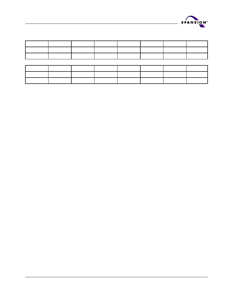
November 5, 2004 S29CD016_00_A4
S29CD016G
27
A d v a n c e I n f o r m a t i o n
Initial Access Delay Configuration
The frequency configuration informs the device of the number of clocks that must
elapse after ADV# is driven active before data is available. This value is deter-
mined by the input clock frequency.
Sector Protection
The device features several levels of sector protection, which can disable both the
program and erase operations in certain sectors or sector groups.
Sector and Sector Groups
The distinction between sectors and sector groups is fundamental to sector pro-
tection. Sector are individual sectors that can be individually sector protected/
unprotected. These are the outermost 4 Kword boot sectors, that is, SA0 to SA7
and SA38 to SA45. See
Table 12 on page 34
and
Table 13 on page 36
.
Sector groups are a collection of three or four adjacent 32 kword sectors. For ex-
ample, sector group SG8 is comprised of sector SA8 to SA10. When any sector in
a sector group is protected/unprotected, every sector in that group is protection/
unprotected. See
Table 12 on page 34
and
Table 13 on page 36
.
Persistent Sector Protection
A command sector protection method that replaces the old 12 V controlled pro-
tection method.
Password Sector Protection
A highly sophisticated protection method that requires a password before
changes to certain sectors or sector groups are permitted.
WP# Hardware Protection
A write protect pin that can prevent program or erase to the two outermost 8
Kbytes sectors in the 75% bank.
All parts default to operate in the Persistent Sector Protection mode. The cus-
tomer must then choose if the Persistent or Password Protection method is most
desirable. There are two one-time programmable non-volatile bits that define
which sector protection method is used. If the customer decides to continue using
the Persistent Sector Protection method, they must set the Persistent Sector
Protection Mode Locking Bit. This permanently sets the part to operate only
using Persistent Sector Protection. If the customer decides to use the password
method, they must set the Password Mode Locking Bit. This permanently sets
the part to operate only using password sector protection.
Table 10. Configuration Register After Device Reset
CR15
CR14
CR13
CR12
CR11
CR10
CR9
CR8
RM
ASD
IAD3
IAD2
IAD1
IAD0
DOC
WC
1
0
0
1
1
1
0
0
CR7
CR6
CR5
CR4
CR3
CR2
CR1
CR0
BS
CC
Reserve
Reserve
Reserve
BL2
BL1
BL0
1
1
0
0
0
1
0
0

28
S29CD016G
S29CD016_00_A4 November 5, 2004
A d v a n c e I n f o r m a t i o n
It is important to remember that setting either the Persistent Sector Protec-
tion Mode Locking Bit or the Password Mode Locking Bit permanently
selects the protection mode. It is not possible to switch between the two methods
once a locking bit is set. It is important that one mode is explicitly selected
when the device is first programmed, rather than relying on the default
mode alone. This is so that it is not possible for a system program or virus to
later set the Password Mode Locking Bit, which would cause an unexpected shift
from the default Persistent Sector Protection Mode into the Password Protection
Mode.
The WP# Hardware Protection feature is always available, independent of the
software managed protection method chosen.
Persistent Sector Protection
The Persistent Sector Protection method replaces the old 12 V controlled protec-
tion method while at the same time enhancing flexibility by providing three
different sector protection states:
Persistently Locked--A sector is protected and cannot be changed.
Dynamically Locked--The sector is protected and can be changed by a sim-
ple command
Unlocked--The sector is unprotected and can be changed by a simple com-
mand
In order to achieve these states, three types of "bits" are going to be used:
Persistent Protection Bit (PPB)
A single Persistent (non-volatile) Protection Bit is assigned to a maximum of four
sectors (see the sector address tables for specific sector protection groupings).
All 8 Kbyte boot-block sectors have individual sector Persistent Protection Bits
(PPBs) for greater flexibility. Each PPB is individually modifiable through the PPB
Write Command.
Note: If a PPB requires erasure, all of the sector PPBs must first be prepro-
grammed prior to PPB erasing. All PPBs erase in parallel, unlike programming
where individual PPBs are programmable. It is the responsibility of the user to
perform the preprogramming operation. Otherwise, an already erased sector
PPBs includes the potential of being over-erased. There is no hardware mecha-
nism to prevent sector PPBs over-erasure.
Persistent Protection Bit Lock (PPB Lock)
A global volatile bit. When set to "1", the PPBs cannot be changed. When cleared
("0"), the PPBs are changeable. There is only one PPB Lock bit per device. The
PPB Lock is cleared after power-up or hardware reset. There is no command se-
quence to unlock the PPB Lock.
Dynamic Protection Bit (DYB)
A volatile protection bit is assigned for each sector. After power-up or hardware
reset, the contents of all DYBs is "0". Each DYB is individually modifiable through
the DYB Write Command.
When the parts are first shipped, the PPBs are cleared, the DYBs are cleared, and
PPB Lock is defaulted to power up in the cleared state ≠ meaning the PPBs are
changeable.
When the device is first powered on the DYBs power up cleared (sectors not pro-
tected). The Protection State for each sector is determined by the logical OR of
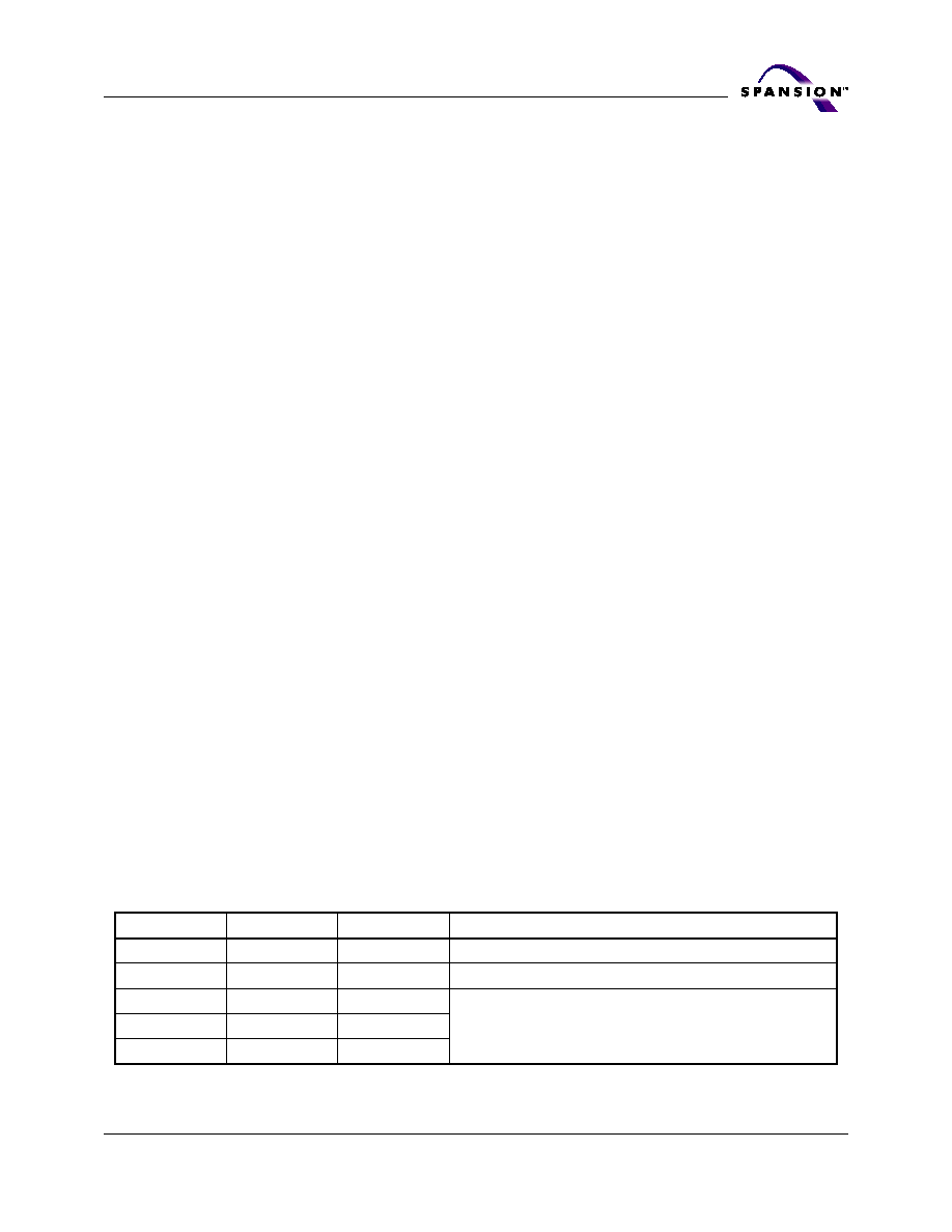
November 5, 2004 S29CD016_00_A4
S29CD016G
29
A d v a n c e I n f o r m a t i o n
the PPB and the DYB related to that sector. For the sectors that have the PPBs
cleared, the DYBs control whether or not the sector is protected or unprotected.
By issuing the DYB Write command sequences, the DYBs are set or cleared, thus
placing each sector in the protected or unprotected state. These are the so-called
Dynamic Locked or Unlocked states. They are called dynamic states because
it is very easy to switch back and forth between the protected and unprotected
conditions. This allows software to easily protect sectors against inadvertent
changes yet does not prevent the easy removal of protection when changes are
needed. The DYBs maybe set or cleared as often as needed.
The PPBs allow for a more static, and difficult to change, level of protection. The
PPBs retain their state across power cycles because they are Non-Volatile. Indi-
vidual PPBs are set with a command but must all be cleared as a group through
a complex sequence of program and erasing commands. The PPBs are limited to
100 erase cycles.
The PPB Lock bit adds an additional level of protection. Once all PPBs are pro-
grammed to the desired settings, the PPB Lock may be set to "1". Setting the PPB
Lock disables all program and erase commands to the Non-Volatile PPBs. In ef-
fect, the PPB Lock Bit locks the PPBs into their current state. The only way to clear
the PPB Lock is to go through a power cycle. System boot code can determine if
any changes to the PPB are needed e.g. to allow new system code to be down-
loaded. If no changes are needed then the boot code can set the PPB Lock to
disable any further changes to the PPBs during system operation.
The WP# write protect pin adds a final level of hardware protection to the two
outermost 8 Kbytes sectors in the 75% bank. When this pin is low it is not pos-
sible to change the contents of these two sectors.
It is possible to have sectors that are persistently locked, and sectors that are left
in the dynamic state. The sectors in the dynamic state are all unprotected. If
there is a need to protect some of them, a simple DYB Write command sequence
is all that is necessary. The DYB write command for the dynamic sectors switch
the DYBs to signify protected and unprotected, respectively. If there is a need to
change the status of the persistently locked sectors, a few more steps are re-
quired. First, the PPB Lock bit must be disabled by either putting the device
through a power-cycle, or hardware reset. The PPBs can then be changed to re-
flect the desired settings. Setting the PPB lock bit once again locks the PPBs, and
the device operates normally again.
Note: to achieve the best protection, it's recommended to execute the PPB lock
bit set command early in the boot code, and protect the boot code by holding
WP# = V
IL
.
Table 11. Sector Protection Schemes (Sheet 1 of 2)
DYB
PPB
PPB Lock
Sector State
0
0
0
Unprotected--PPB and DYB are changeable
0
0
1
Unprotected--PPB not changeable, DYB is changeable
0
1
0
Protected--PPB and DYB are changeable
1
0
0
1
1
0
30
S29CD016G
S29CD016_00_A4 November 5, 2004
A d v a n c e I n f o r m a t i o n
Table 11
contains all possible combinations of the DYB, PPB, and PPB lock relating
to the status of the sector.
In summary, if the PPB is set, and the PPB lock is set, the sector is protected and
the protection can not be removed until the next power cycle clears the PPB lock.
If the PPB is cleared, the sector can be dynamically locked or unlocked. The DYB
then controls whether or not the sector is protected or unprotected.
If the user attempts to program or erase a protected sector, the device ignores
the command and returns to read mode. A program command to a protected sec-
tor enables status polling for approximately 1 µs before the device returns to read
mode without having modified the contents of the protected sector. An erase
command to a protected sector enables status polling for approximately 50 µs
after which the device returns to read mode without having erased the protected
sector.
The programming of the DYB, PPB, and PPB lock for a given sector can be verified
by writing a DYB/PPB/PPB lock verify command to the device.
Persistent Sector Protection Mode Locking Bit
Like the password mode locking bit, a Persistent Sector Protection mode locking
bit exists to guarantee that the device remain in software sector protection. Once
set, the Persistent Sector Protection locking bit prevents programming of the
password protection mode locking bit. This guarantees that an unauthorized user
could not place the device in password protection mode.
Password Protection Mode
The Password Sector Protection Mode method allows an even higher level of se-
curity than the Persistent Sector Protection Mode. There are two main differences
between the Persistent Sector Protection and the Password Sector Protection
Mode:
When the device is first powered on, or comes out of a reset cycle, the PPB
Lock bit set to the locked state, rather than cleared to the unlocked state.
The only means to clear the PPB Lock bit is by writing a unique 64-bit Pass-
word to the device.
The Password Sector Protection method is otherwise identical to the Persistent
Sector Protection method.
A 64-bit password is the only additional tool utilized in this method.
The password is stored in a one-time programmable (OTP) region of the flash
memory. Once the Password Mode Locking Bit is set, the password is perma-
nently set with no means to read, program, or erase it. The password is used to
clear the PPB Lock bit. The Password Unlock command must be written to the
flash, along with a password. The flash device internally compares the given
password with the pre-programmed password. If they match, the PPB Lock bit is
cleared, and the PPBs can be altered. If they do not match, the flash device does
nothing. There is a built-in 2 µs delay for each "password check." This delay is
0
1
1
Protected--PPB not changeable, DYB is changeable
1
0
1
1
1
1
Table 11. Sector Protection Schemes (Sheet 2 of 2)
DYB
PPB
PPB Lock
Sector State

November 5, 2004 S29CD016_00_A4
S29CD016G
31
A d v a n c e I n f o r m a t i o n
intended to thwart any efforts to run a program that tries all possible combina-
tions in order to crack the password.
Password and Password Mode Locking Bit
In order to select the Password sector protection scheme, the customer must first
program the password. One method of choosing a password would be to correlate
it to the unique Electronic Serial Number (ESN) of the particular flash device. An-
other method could generate a database where all the passwords are stored,
each of which correlates to a serial number on the device. Each ESN is different
for every flash device; therefore each password should be different for every flash
device. While programming in the password region, the customer may perform
Password Verify operations.
Once the desired password is programmed in, the customer must then set the
Password Mode Locking Bit. This operation achieves two objectives:
1) It permanently sets the device to operate using the Password Protection Mode.
It is not possible to reverse this function.
2) It also disables all further commands to the password region. All program, and
read operations are ignored.
Both of these objectives are important, and if not carefully considered, may lead
to unrecoverable errors. The user must be sure that the Password Protection
method is desired when setting the Password Mode Locking Bit. More importantly,
the user must be sure that the password is correct when the Password Mode
Locking Bit is set. Due to the fact that read operations are disabled, there is no
means to verify what the password is afterwards. If the password is lost after set-
ting the Password Mode Locking Bit, there is no way to clear the PPB Lock bit.
The Password Mode Locking Bit, once set, prevents reading the 64-bit password
on the DQ bus and further password programming. The Password Mode Locking
Bit is not erasable. Once Password Mode Locking Bit is programmed, the Persis-
tent Sector Protection Locking Bit is disabled from programming, guaranteeing
that no changes to the protection scheme are allowed.
64-bit Password
The 64-bit Password is located in its own memory space and is accessible through
the use of the Password Program and Verify commands (see
"Password Verify
Command" on page 53
). The password function works in conjunction with the
Password Mode Locking Bit, which when set, prevents the Password Verify com-
mand from reading the contents of the password on the pins of the device.

32
S29CD016G
S29CD016_00_A4 November 5, 2004
A d v a n c e I n f o r m a t i o n
Write Protect (WP#)
The device features a hardware protection option using a write protect pin that
prevents programming or erasing, regardless of the state of the sector's Persis-
tent or Dynamic Protection Bits. The WP# pin is associated with the two
outermost 8Kbytes sectors in the 75% bank. The WP# pin has no effect on any
other sector. When WP# is taken to V
IL
, programming and erase operations of the
two outermost 8 Kbytes sectors in the 75% bank are disabled. By taking WP#
back to V
IH
, the two outermost 8 Kbytes sectors are enabled for program and
erase operations, depending upon the status of the individual sector Persistent or
Dynamic Protection Bits. If either of the two outermost sectors Persistent or Dy-
namic Protection Bits are programmed, program or erase operations are
inhibited. If the sector Persistent or Dynamic Protection Bits are both erased, the
two sectors are available for programming or erasing as long as WP# remains at
V
IH
. The user must hold the WP# pin at either V
IH
or V
IL
during the entire pro-
gram or erase operation of the two outermost sectors in the 75% bank.
SecSiTM (Secured Silicon) Sector Protection
The SecSi Sector is a 256-byte flash memory area that is either programmable
at the customer or by AMD at the request of the customer. The SecSi Sector Entry
command enables the host system to address the SecSi Sector for programming
or reading. The SecSi sector address range is 00000h≠0003Fh for the ordering
option 00 and 7FFC0h≠7FFFFh for the ordering option 01. Address range
00040h≠007FFh for ordering option 0 and 7F800h≠7FFBFh for ordering option 01
return invalid data when addressed with the SecSi Sector enabled.
The device allows Simultaneous Read/Write operation while the SecSi Sector is
enabled. However, there are a number of restrictions associated with Simulta-
neous Read/Write operations and device operation when the SecSi Sector is
enabled:
1) The SecSi Sector is not available for reading while the Password Unlock, any
PPB program/erase operation, or Password programming are in progress.
Reading to any location in the small (25%) sector returns the status of these
operations until these operations have completed execution.
2) Writing the corresponding DYB associated with the overlaid bootblock sector
results in the DYB NOT being updated. This is only accomplished when the
SecSi sector is not enabled.
3) Reading the corresponding DYB associated with the overlaid bootblock sector
results in reading invalid data when the PPB Lock/DYB Verify command is is-
sued. This function is only accomplished when the SecSi Sector is not
enabled.
4) All commands are available for execution when the SecSi Sector is enabled
except the following list. Issuing the following commands while the SecSi
Sector is enabled results in the command being ignored.
All Unlock Bypass commands
CFI
Accelerated Program
Program and Sector Erase Suspend
Program and Sector Erase Resume
5) Executing the Sector Erase command is permitted when the SecSi Sector is
enabled, however, there is no provision for erasing the SecSi Sector with the

November 5, 2004 S29CD016_00_A4
S29CD016G
33
A d v a n c e I n f o r m a t i o n
Sector Erase command, regardless of the protection status. The Sector Erase
command erases all other sectors when the SecSi Sector is enabled.
6) Executing the Chip Erase command is permitted when the SecSi Sector is en-
abled. The Chip Erase command erases all sectors in the memory array
except for sector 0 in top-bootblock configuration and sector 45 in bottom-
bootblock configuration. The SecSi Sector is a one-time programmable mem-
ory area that cannot be erased.
7) Executing the SecSi Sector Entry command during program or erase suspend
mode is allowed. The Sector Erase/Program Resume command is disabled
while the SecSi sector is enabled, and the user cannot resume programming
of the memory array until the Exit SecSi Sector command is written.
SecSi Sector Protection Bit
The SecSi Sector Protection Bit prevents programming of the SecSi Sector mem-
ory area. Once set, the SecSi Sector memory area contents are non-modifiable.
Persistent Protection Bit Lock
The Persistent Protection Bit (PPB) Lock is a volatile bit that reflects the state of
the Password Mode Locking Bit after power-up reset. If the Password Mode Lock-
ing Bit is set, which indicates the device is in Password Protection Mode, the PPB
Lock Bit is also set after a hardware reset (RESET# asserted) or a power-up reset.
The ONLY means for clearing the PPB Lock Bit in Password Protection Mode is to
issue the Password Unlock command. Successful execution of the Password Un-
lock command clears the PPB Lock Bit, allowing for sector PPBs modifications.
Asserting RESET#, taking the device through a power-on reset, or issuing the
PPB Lock Bit Set command sets the PPB Lock Bit back to a "1".
If the Password Mode Locking Bit is not set, indicating Persistent Sector Protec-
tion Mode, the PPB Lock Bit is cleared after power-up or hardware reset. The PPB
Lock Bit is set by issuing the PPB Lock Bit Set command. Once set the only means
for clearing the PPB Lock Bit is by issuing a hardware or power-up reset. The
Password Unlock command is ignored in Persistent Sector Protection Mode.
Hardware Data Protection
The command sequence requirement of unlock cycles for programming or erasing
provides data protection against inadvertent writes. In addition, the following
hardware data protection measures prevent accidental erasure or programming,
which might otherwise be caused by spurious system level signals during V
CC
power-up and power-down transitions, or from system noise.
Low V
CC
Write Inhibit
When V
CC
is less than V
LKO
, the device does not accept any write cycles. This pro-
tects data during V
CC
power-up and power-down. The command register and all
internal erase/program circuits are disabled, and the device resets. Subsequent
writes are ignored until V
CC
is greater than V
LKO
. The system must provide the
proper signals to the control pins to prevent unintentional writes when V
CC
is
greater than V
LKO
.
Write Pulse "Glitch" Protection
Noise pulses of less than 5 ns (typical) on OE#, CE#, or WE# do not initiate a
write cycle.
34
S29CD016G
S29CD016_00_A4 November 5, 2004
A d v a n c e I n f o r m a t i o n
Logical Inhibit
Write cycles are inhibited by holding any one of OE# = V
IL
, CE# = V
IH
, or WE#
= V
IH
. To initiate a write cycle, CE# and WE# must be a logical zero (V
IL
) while
OE# is a logical one (V
IH
).
Power-Up Write Inhibit
If WE# = CE# = V
IL
and OE# = V
IH
during power-up, the device does not accept
commands on the rising edge of WE#. The internal state machine is automatically
reset to reading array data on power-up.
V
CC
and V
IO
Power-up And Power-down Sequencing
The device imposes no restrictions on V
CC
and V
IO
power-up or power-down se-
quencing. Asserting RESET# to V
IL
is required during the entire V
CC
and V
IO
power sequence until the respective supplies reach their operating voltages.
Once, V
CC
and V
IO
attain their respective operating voltages, de-assertion of RE-
SET# to V
IH
is permitted.
Table 12. Sector Addresses for Ordering Option 00 (Sheet 1 of 2)
Sector
Sector Group
x32
Address Range (A18:A0)
Sector Size
(KDwords)
Ba
nk
0 (
N
o
t
e
2)
SA0 (Note 1)
SG0
00000h≠007FFh
2
SA1 SG1
00800h≠00FFFh
2
SA2
SG2
01000h≠017FFh
2
SA3
SG3
01800h≠01FFFh
2
SA4
SG4
02000h≠027FFh
2
SA5
SG5
02800h≠02FFFh
2
SA6
SG6
03000h≠037FFh
2
SA7
SG7
03800h≠03FFFh
2
SA8
SG8
04000h≠07FFFh
16
SA9
08000h≠0BFFFh
16
SA10
0C000h≠0FFFFh
16
SA11
SG9
10000h≠13FFFh
16
SA12
14000h≠17FFFh
16
SA13
18000h≠1BFFFh
16
SA14
1C000h≠1FFFFh
16
November 5, 2004 S29CD016_00_A4
S29CD016G
35
A d v a n c e I n f o r m a t i o n
1. SecSi Sector overlays this sector when enabled.
2. The bank address is determined by A18 and A17. BA = 00 for Bank 1 and BA = 01, 10, or 11 for Bank 2.
3. This sector includes the additional WP# pin sector protection feature.
Ban
k
1
(Not
e
2
)
SA15
SG10
20000h≠23FFFh
16
SA16
24000h≠27FFFh
16
SA17
28000h≠2BFFFh
16
SA18
2C000h≠2FFFFh
16
SA19
SG11
30000h≠33FFFh
16
SA20
34000h≠37FFFh
16
SA21
38000h≠3BFFFh
16
SA22
3C000h≠3FFFFh
16
SA23
SG12
40000h≠43FFFh
16
SA24
44000h≠47FFFh
16
SA25
48000h≠4BFFFh
16
SA26
4C000h≠4FFFFh
16
SA27
SG13
50000h≠53FFFh
16
SA28
54000h≠57FFFh
16
SA29
58000h≠5BFFFh
16
SA30
5C000h≠5FFFFh
16
SA31
SG14
60000h≠63FFFh
16
SA32
64000h≠67FFFh
16
SA33
68000h≠6BFFFh
16
SA34
6C000h≠6FFFFh
16
SA35
SG15
70000h≠73FFFh
16
SA36
74000h≠77FFFh
16
SA37
78000h≠7BFFFh
16
SA38
SG16
7C000h≠7C7FFh
2
SA39
SG17
7C800h≠7CFFFh
2
SA40
SG18
7D000h≠7D7FFh
2
SA41
SG19
7D800h≠7DFFFh
2
SA42
SG20
7E000h≠7E7FFh
2
SA43
SG21
7E800h≠7EFFFh
2
SA44 (Note 3)
SG22
7F000h≠7F7FFh
2
SA45 (Note 3)
SG23
7F800h≠7FFFFh
2
Table 12. Sector Addresses for Ordering Option 00 (Sheet 2 of 2)
Sector
Sector Group
x32
Address Range (A18:A0)
Sector Size
(KDwords)
36
S29CD016G
S29CD016_00_A4 November 5, 2004
A d v a n c e I n f o r m a t i o n
Table 13. Sector Addresses for Ordering Option 01 (Sheet 1 of 2)
Sector
Sector Group
x32
Address Range (A18:A0)
Sector Size
(KDwords)
Ba
n
k
0 (
N
ot
e
2
)
SA0 (Note 1)
SG0
00000h≠007FFh
2
SA1 (Note 1)
SG1
00800h≠00FFFh
2
SA2
SG2
01000h≠017FFh
2
SA3
SG3
01800h≠01FFFh
2
SA4
SG4
02000h≠027FFh
2
SA5
SG5
02800h≠02FFFh
2
SA6
SG6
03000h≠037FFh
2
SA7
SG7
03800h≠03FFFh
2
SA8
SG8
04000h≠07FFFh
16
SA9
08000h≠0BFFFh
16
SA10
0C000h≠0FFFFh
16
SA11
SG9
10000h≠13FFFh
16
SA12
14000h≠17FFFh
16
SA13
18000h≠1BFFFh
16
SA14
1C000h≠1FFFFh
16
SA15
SG10
20000h≠23FFFh
16
SA16
24000h≠27FFFh
16
SA17
28000h≠2BFFFh
16
SA18
2C000h≠2FFFFh
16
SA19
SG11
30000h≠33FFFh
16
SA20
34000h≠37FFFh
16
SA21
38000h≠3BFFFh
16
SA22
3C000h≠3FFFFh
16
SA23
SG12
40000h≠43FFFh
16
SA24
44000h≠47FFFh
16
SA25
48000h≠4BFFFh
16
SA26
4C000h≠4FFFFh
16
SA27
SG13
50000h≠53FFFh
16
SA28
54000h≠57FFFh
16
SA29
58000h≠5BFFFh
16
SA30
5C000h≠5FFFFh
16
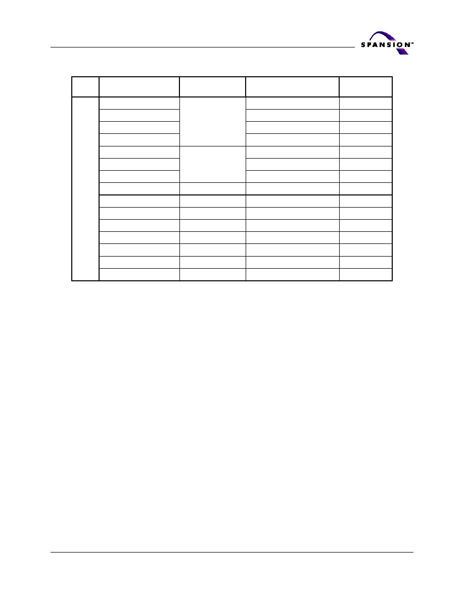
November 5, 2004 S29CD016_00_A4
S29CD016G
37
A d v a n c e I n f o r m a t i o n
1. This sector includes the additional WP# pin sector protection feature.
2. The bank address is determined by A18 and A17. BA = 00, 01, or 10 for Bank 0 and BA = 11 for Bank 1.
3. SecSi Sector overlays this sector when enabled.
Ba
n
k
1
(Not
e
2
)
SA31
SG14
60000h≠63FFFh
16
SA32
64000h≠67FFFh
16
SA33
68000h≠6BFFFh
16
SA34
6C000h≠6FFFFh
16
SA35
SG15
70000h≠73FFFh
16
SA36
74000h≠77FFFh
16
SA37
78000h≠7BFFFh
16
SA38
SG16
7C000h≠7C7FFh
2
SA39
SG17
7C800h≠7CFFFh
2
SA40
SG18
7D000h≠7D7FFh
2
SA41
SG19
7D800h≠7DFFFh
2
SA42
SG20
7E000h≠7E7FFh
2
SA43
SG21
7E800h≠7EFFFh
2
SA44
SG22
7F000h≠7F7FFh
2
SA45 (Note 3)
SG23
7F800h≠7FFFFh
2
Table 13. Sector Addresses for Ordering Option 01 (Sheet 2 of 2)
Sector
Sector Group
x32
Address Range (A18:A0)
Sector Size
(KDwords)
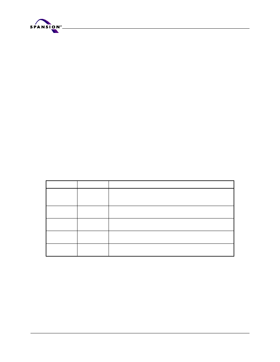
38
S29CD016G
S29CD016_00_A4 November 5, 2004
A d v a n c e I n f o r m a t i o n
Common Flash Memory Interface (CFI)
The Common Flash Interface (CFI) specification outlines device and host system
software interrogation handshake, which allows specific vendor-specified soft-
ware algorithms to be used for entire families of devices. Software support can
then be device-independent, JEDEC ID-independent, and forward- and back-
ward-compatible for the specified flash device families. Flash vendors can
standardize their existing interfaces for long-term compatibility.
This device enters the CFI Query mode when the system writes the CFI Query
command, 98h, to address 55h in word mode (or address AAh in byte mode), any
time the device is ready to read array data. The system can read CFI information
at the addresses given in
Table 14 on page 38
to
TTable 17 on page 41
. To ter-
minate reading CFI data, the system must write the reset command.
The system can also write the CFI query command when the device is in the au-
toselect mode. The device enters the CFI query mode, and the system can read
CFI data at the addresses given in
Table 14 on page 38
to
TTable 17 on page 41
.
The system must write the reset command to return the device to the autoselect
mode.
For further information, please refer to the CFI Specification and CFI Publication
100, available via the World Wide Web at http://www.amd.com/products/nvd/
overview/cfi.html. Alternatively, contact a Spansion representative for copies of
these documents.
Note: CFI cannot be read in synchronous mode.
Table 14. CFI Query Identification String
Addresses
Data
Description
10h
11h
12h
0051h
0052h
0059h
Query Unique ASCII string "QRY"
13h
14h
0002h
0000h
Primary OEM Command Set
15h
16h
0040h
0000h
Address for Primary Extended Table
17h
18h
0000h
0000h
Alternate OEM Command Set (00h = none exists)
19h
1Ah
0000h
0000h
Address for Alternate OEM Extended Table (00h = none exists)
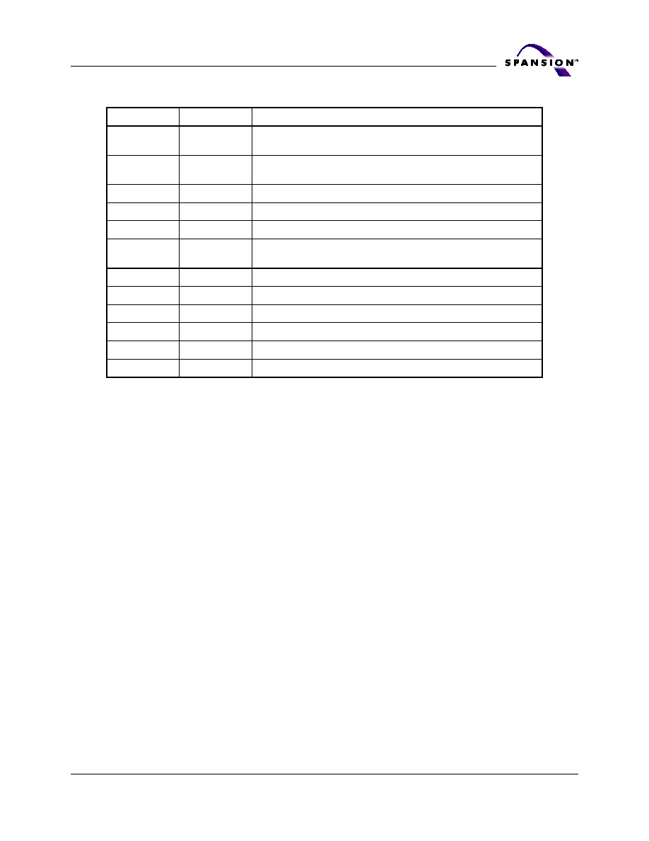
November 5, 2004 S29CD016_00_A4
S29CD016G
39
A d v a n c e I n f o r m a t i o n
Table 15. CFI System Interface String
Addresses
Data
Description
1Bh
0023h
V
CC
Min. (write/erase)
DQ7≠DQ4: volts, DQ3≠DQ0: 100 millivolt
1Ch
0027h
V
CC
Max. (write/erase)
DQ7≠DQ4: volts, DQ3≠DQ0: 100 millivolt
1Dh
0000h
V
PP
Min. voltage (00h = no V
PP
pin present)
1Eh
0000h
V
PP
Max. voltage (00h = no V
PP
pin present)
1Fh
0004h
Typical timeout per single word/doubleword program 2
N
µs
20h
0000h
Typical timeout for Min. size buffer program 2
N
µs (00h = not
supported)
21h
0009h
Typical timeout per individual block erase 2
N
ms
22h
0000h
Typical timeout for full chip erase 2
N
ms (00h = not supported)
23h
0005h
Max. timeout for word/doubleword program 2
N
times typical
24h
0000h
Max. timeout for buffer write 2
N
times typical
25h
0007h
Max. timeout per individual block erase 2
N
times typical
26h
0000h
Max. timeout for full chip erase 2
N
times typical (00h = not supported)
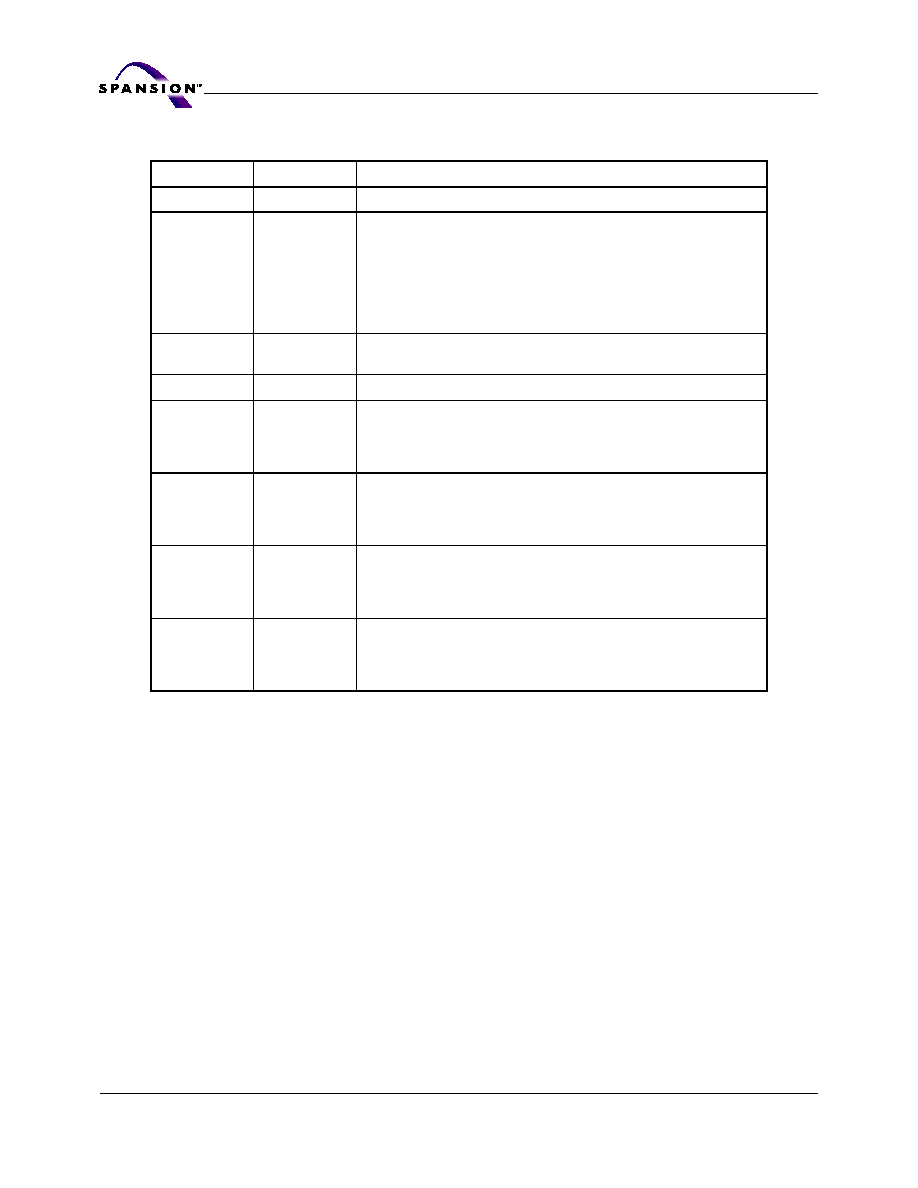
40
S29CD016G
S29CD016_00_A4 November 5, 2004
A d v a n c e I n f o r m a t i o n
Table 16. Device Geometry Definition
Addresses
Data
Description
27h
0015h
Device Size = 2
N
byte
28h
29h
0003h
0000h
Flash Device Interface description (for complete description, please
refer to CFI publication 100)
0000 = x8-only asynchronous interface
0001 = x16-only asynchronous interface
0002 = supports x8 and x16 via BYTE# with asynchronous interface
0003 = x 32-only asynchronous interface
2Ah
2Bh
0000h
0000h
Max. number of byte in multi-byte program = 2
N
(00h = not supported)
2Ch
0003h
Number of Erase Block Regions within device
2Dh
2Eh
2Fh
30h
0007h
0000h
0020h
0000h
Erase Block Region 1 Information
(refer to the CFI specification or CFI publication 100)
31h
32h
33h
34h
001Dh
0000h
0000h
0001h
Erase Block Region 2 Information
(refer to the CFI specification or CFI publication 100)
35h
36h
37h
38h
0007h
0000h
0020h
0000h
Erase Block Region 3 Information
(refer to the CFI specification or CFI publication 100)
39h
3Ah
3Bh
3Ch
0000h
0000h
0000h
0000h
Erase Block Region 4 Information
(refer to the CFI specification or CFI publication 100)
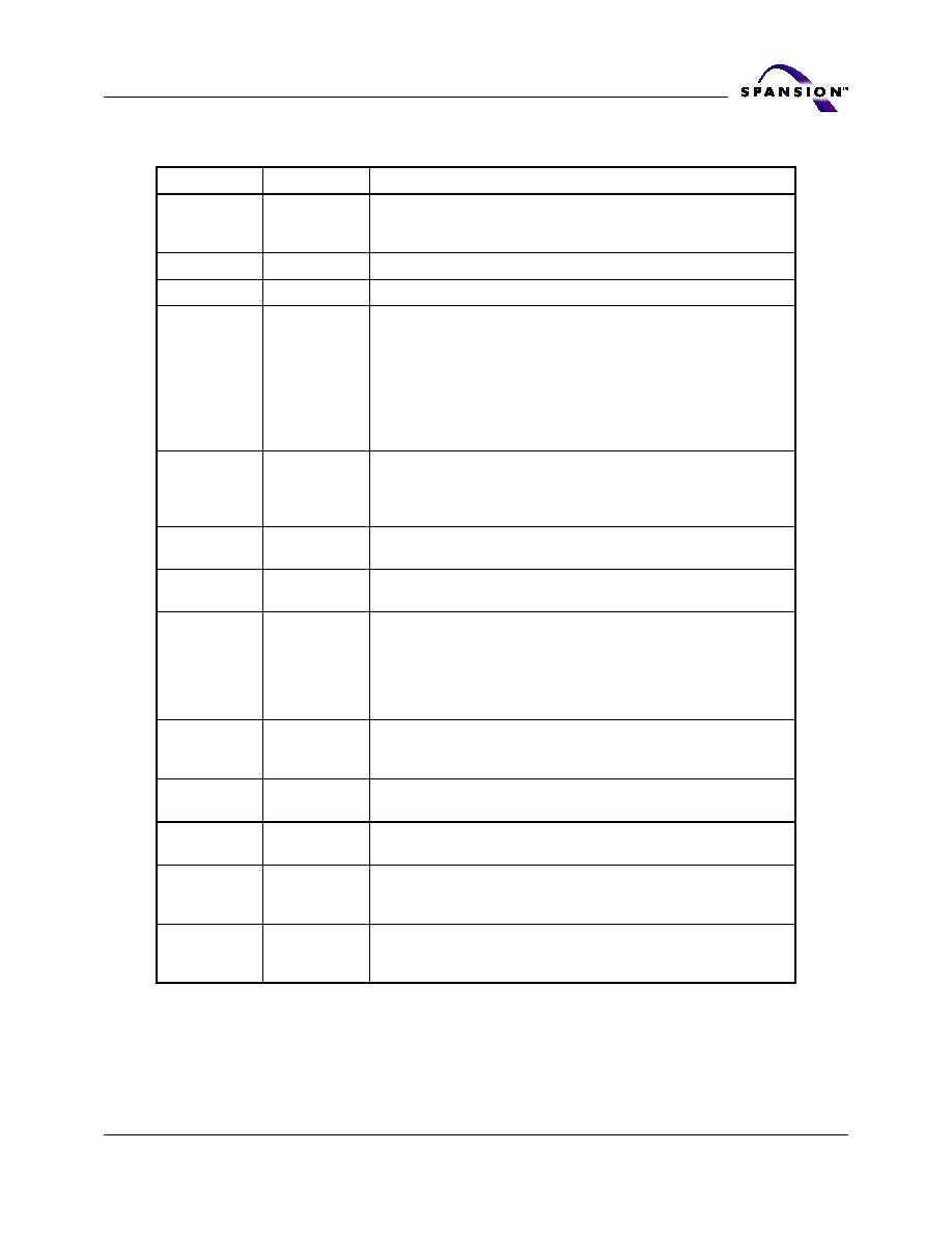
November 5, 2004 S29CD016_00_A4
S29CD016G
41
A d v a n c e I n f o r m a t i o n
Table 17. CFI Primary Vendor-Specific Extended Query (Sheet 1 of 2)
Addresses
Data
Description
40h
41h
42h
0050h
0052h
0049h
Query-unique ASCII string "PRI"
43h
0031h
Major version number, ASCII (reflects modifications to the silicon)
44h
0033h
Minor version number, ASCII (reflects modifications to the CFI table)
45h
0004h
Address Sensitive Unlock (DQ1, DQ0)
00 = Required, 01 = Not Required
Silicon Revision Number (DQ5≠DQ2
0000 = CS49
0001 = CS59
0010 = CS99
0011 = CS69
0100 = CS119
46h
0002h
Erase Suspend (1 byte)
00 = Not Supported
01 = To Read Only
02 = To Read and Write
47h
0001h
Sector Protect (1 byte)
00 = Not Supported, X = Number of sectors in per group
48h
0000h
Temporary Sector Unprotect
00h = Not Supported, 01h = Supported
49h
0006h
Sector Protect/Unprotect scheme (1 byte)
01 =29F040 mode, 02 = 29F016 mode
03 = 29F400 mode, 04 = 29LV800 mode
05 = 29BDS640 mode (Software Command Locking)
06 = BDD160 mode (New Sector Protect)
07 = 29LV800 + PDL128 (New Sector Protect) mode
4Ah
001Fh
Simultaneous Read/Write (1 byte)
00h = Not Supported, X = Number of sectors in all banks except
Bank 1
4Bh
0001h
Burst Mode Type
00h = Not Supported, 01h = Supported
4Ch
0000h
Page Mode Type
00h = Not Supported, 01h = 4 Word Page, 02h = 8 Word Page
4Dh
00B5h
ACC (Acceleration) Supply Minimum
00h = Not Supported (DQ7-DQ4: volt in hex, DQ3-DQ0: 100 mV in
BCD)
4Eh
00C5h
ACC (Acceleration) Supply Maximum
00h = Not Supported, (DQ7-DQ4: volt in hex, DQ3-DQ0: 100 mV in
BCD)
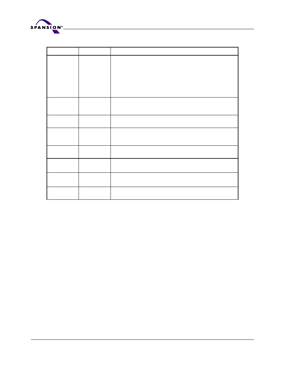
42
S29CD016G
S29CD016_00_A4 November 5, 2004
A d v a n c e I n f o r m a t i o n
4Fh
0001h
Top/Bottom Boot Sector Flag (1 byte)
00h = Uniform device, no WP# control,
01h = 8 x 8 Kb sectors at top and bottom with WP# control
02h = Bottom boot device
03h = Top boot device
04h = Uniform, Bottom WP# Protect
05h = Uniform, Top WP# Protect
If the number of erase block regions = 1, then ignore this field
50h
0001h
Program Suspend
00 = Not Supported
01 = Supported
51h 0000h
Write Buffer Size
2
(N+1)
word(s)
57h
0002h
Bank Organization (1 byte)
00 = If data at 4Ah is zero
XX = Number of banks
58h
000Fh
Bank 1 Region Information (1 byte)
XX = Number of Sectors in Bank 1
59h
001Fh
Bank 2 Region Information (1 byte)
XX = Number of Sectors in Bank 2
5Ah
0000h
Bank 3 Region Information (1 byte)
XX = Number of Sectors in Bank 3
5Bh
0000h
Bank 4 Region Information (1 byte)
XX = Number of Sectors in Bank 4
Table 17. CFI Primary Vendor-Specific Extended Query (Sheet 2 of 2)
Addresses
Data
Description

November 5, 2004 S29CD016_00_A4
S29CD016G
43
A d v a n c e I n f o r m a t i o n
Command Definitions
Writing specific address and data commands or sequences into the command
register initiates device operations. Tables 8
-
9 define the valid register command
sequences. Writing incorrect address and data values or writing them in the
improper sequence resets the device to reading array data.
All addresses are latched on the falling edge of WE# or CE#, whichever happens
later. All data is latched on the rising edge of WE# or CE#, whichever happens
first. Refer to
"AC Characteristics" on page 70
for timing diagrams.
Reading Array Data in Non-burst Mode
The device is automatically set to reading array data after device power-up. No
commands are required to retrieve data. The device is also ready to read array
data after completing an Embedded Program or Embedded Erase algorithm.
After the device accepts an Erase Suspend command, the device enters the Erase
Suspend mode. The system can read array data using the standard read timings,
except that if it reads at an address within erase-suspended sectors, the device
outputs status data. After completing a programming operation in the Erase Sus-
pend mode, the system may once again read array data with the same exception.
See
"Sector Erase and Program Suspend Command" on page 49
for more infor-
mation on this mode.
The system must issue the reset command to re-enable the device for reading
array data if DQ5 goes high, or while in the autoselect mode.
See also
"Asynchronous Read Operation (Non-Burst)" on page 19
for more
information. See
"Sector Erase and Program Resume Command" on page 51
for
more information on this mode.
Reading Array Data in Burst Mode
The device is capable of very fast Burst mode read operations. The configuration
register sets the read configuration, burst order, frequency configuration, and
burst length.
Upon power on, the device defaults to the asynchronous mode. In this mode,
CLK, and ADV# are ignored. The device operates like a conventional Flash device.
Data is available t
ACC
/t
CE
nanoseconds after address becomes stable, CE# be-
come asserted. The device enters the burst mode by enabling synchronous burst
reads in the configuration register. The device exits burst mode by disabling syn-
chronous burst reads in the configuration register. (See
"Command Definitions"
on page 43
). The RESET# command does not terminate the Burst mode. System
reset (power on reset) terminates the Burst mode.
The device contains the regular control pins, i.e. Chip Enable (CE#), Write Enable
(WE#), and Output Enable (OE#) to control normal read and write operations.
Moreover, three additional control pins were added to allow easy interface with
minimal glue logic to a wide range of microprocessors / microcontrollers for high
performance Burst read capability. These additional pins are Address Valid
(ADV#) and Clock (CLK). CE#, OE#, and WE# are asynchronous (relative to
CLK). The Burst mode read operation is a synchronous operation tied to the edge
of the clock. The microprocessor / microcontroller supplies only the initial ad-
dress, all subsequent addresses are automatically generated by the device with
a timing defined by the Configuration Register definition. The Burst read cycle
consists of an address phase and a corresponding data phase.

44
S29CD016G
S29CD016_00_A4 November 5, 2004
A d v a n c e I n f o r m a t i o n
During the address phase, the Address Valid (ADV#) pin is asserted (taken Low)
for one clock period. Together with the edge of the CLK, the starting burst address
is loaded into the internal Burst Address Counter. The internal Burst Address
Counter can be configured to either the Linear modes (See
"Initial Access Delay
Configuration" on page 27
).
During the data phase, the first burst data is available after the initial access time
delay defined in the Configuration Register. For subsequent burst data, every ris-
ing (or falling) edge of the CLK triggers the output data with the burst output
delay and sequence defined in the Configuration Register.
Tables 8≠9 show all the commands executed by the device. The device automat-
ically powers up in the read/reset state. It is not necessary to issue a read/reset
command after power-up or hardware reset.
Read/Reset Command
After power-up or hardware reset, the device automatically enter the read state.
It is not necessary to issue the reset command after power-up or hardware reset.
Standard microprocessor cycles retrieve array data, however, after power-up,
only asynchronous accesses are permitted since the Configuration Register is at
its reset state with burst accesses disabled.
The Reset command is executed when the user needs to exit any of the other user
command sequences (such as autoselect, program, chip erase, etc.) to return to
reading array data. There is no latency between executing the Reset command
and reading array data.
The Reset command does not disable the SecSi sector if it is enabled. This func-
tion is only accomplished by issuing the SecSi Sector Exit command.
Autoselect Command
Flash memories are intended for use in applications where the local CPU alters
memory contents. As such, manufacturer and device codes must be accessible
while the device resides in the target system. PROM programmers typically ac-
cess the signature codes by raising A9 to V
ID
. However, multiplexing high voltage
onto the address lines is not generally desired system design practice.
The device contains an Autoselect Command operation to supplement traditional
PROM programming methodology. The operation is initiated by writing the Au-
toselect command sequence into the command register. The bank address (BA)
is latched during the autoselect command sequence write operation to distinguish
which bank the Autoselect command references. Reading the other bank after the
Autoselect command is written results in reading array data from the other bank
and the specified address. Following the command write, a read cycle from ad-
dress (BA)XX00h retrieves the manufacturer code of (BA)XX01h. Three
sequential read cycles at addresses (BA) XX01h, (BA) XX0Eh, and (BA) XX0Fh
read the three-byte device ID (see Table 8).
(The Autoselect Command requires the user to execute the Read/Reset command
to return the device back to reading the array contents.)
Program Command Sequence
Programming is a four-bus-cycle operation. The program command sequence is
initiated by writing two unlock write cycles, followed by the program set-up com-
mand. The program address and data are written next, which in turn initiate the
Embedded Program algorithm. The system is not required to provide further con-

November 5, 2004 S29CD016_00_A4
S29CD016G
45
A d v a n c e I n f o r m a t i o n
trols or timings. The device automatically generates the program pulses and
verifies the programmed cell margin. Tables 8 and 9 show the address and data
requirements for the program command sequence.
During the Embedded Program algorithm, the system can determine the status
of the program operation by using DQ7, DQ6, or RY/BY#. (See
"Write Operation
Status" on page 60
for information on these status bits.) When the Embedded
Program algorithm is complete, the device returns to reading array data and ad-
dresses are no longer latched. Note that an address change is required to begin
read valid array data.
Except for Program Suspend, any commands written to the device during the Em-
bedded Program Algorithm are ignored. Note that a hardware reset
immediately terminates the programming operation. The command sequence
should be reinitiated once that bank returns to reading array data, to ensure data
integrity.
Programming is allowed in any sequence and across sector boundaries. A bit
cannot be programmed from a "0" back to a "1". Attempting to do so may
halt the operation and set DQ5 to "1," or cause the Data# Polling algorithm to
indicate the operation was successful. However, a succeeding read shows that the
data is still "0". Only erase operations can convert a "0" to a "1".
Accelerated Program Command
The Accelerated Chip Program mode is designed to improve the Word or Double
Word programming speed. Improving the programming speed is accomplished by
using the ACC pin to supply both the wordline voltage and the bitline current in-
stead of using the V
PP
pump and drain pump, which is limited to 2.5 mA. Because
the external ACC pin is capable of supplying significantly large amounts of current
compared to the drain pump, all 32 bits are available for programming with a sin-
gle programming pulse. This is an enormous improvement over the standard 5-
bit programming. If the user is able to supply an external power supply and con-
nect it to the ACC pin, significant time savings are realized.
In order to enter the Accelerated Program mode, the ACC pin must first be taken
to V
HH
(12 V ± 0.5 V) and followed by the one-cycle command with the program
address and data to follow. The Accelerated Chip Program command is only exe-
cuted when the device is in Unlock Bypass mode and during normal read/reset
operating mode.
In this mode, the write protection function is bypassed unless the PPB Lock Bit =
1.
The Accelerated Program command is not permitted if the SecSi sector is
enabled.
Unlock Bypass Command Sequence
The unlock bypass feature allows the system to program words to the device
faster than using the standard program command sequence. The unlock bypass
command sequence is initiated by first writing two unlock cycles. This is followed
by a third write cycle containing the unlock bypass command, 20h. The device
then enters the unlock bypass mode. A two-cycle unlock bypass program com-
mand sequence is all that is required to program in this mode. The first cycle in
this sequence contains the unlock bypass program command, A0h; the second
cycle contains the program address and data. Additional data is programmed in
the same manner. This mode dispenses with the initial two unlock cycles required

46
S29CD016G
S29CD016_00_A4 November 5, 2004
A d v a n c e I n f o r m a t i o n
in the standard program command sequence, resulting in faster total program-
ming time.
Figure 19, on page 58
and
Figure 20, on page 59
show the
requirements for the command sequence.
During the unlock bypass mode, only the Unlock Bypass Program and Unlock By-
pass Reset commands are valid. To exit the unlock bypass mode, the system
must issue the two-cycle unlock bypass reset command sequence. The first cycle
must contain the data 90h; the second cycle the data 00h. Addresses are don't
care for both cycles. The device then returns to reading array data.
Figure 4
illustrates the algorithm for the program operation. See
Table 29 on
page 85
for parameters, and
Figure 21, on page 78
and
Figure 22, on page 79
for timing diagrams.
Unlock Bypass Entry Command
The Unlock Bypass command, once issued, is used to bypass the "unlock" se-
quence for program, chip erase, and CFI commands. This feature permits slow
PROM programmers to significantly improve programming/erase throughput
since the command sequence often requires microseconds to execute a single
write operation. Therefore, once the Unlock Bypass command is issued, only the
two-cycle program and erase bypass commands are required. The Unlock Bypass
Command is ignored if the SecSi sector is enabled. To return back to normal op-
eration, the Unlock Bypass Reset Command must be issued.
START
Write Program
Command Sequence
Data Poll
from System
Verify Data?
No
Yes
Last Address?
No
Yes
Programming
Completed
Increment Address
Embedded
Program
algorithm
in progress
Note: See Tables 8 and 9 for program command sequence.
Figure 4. Program Operation

November 5, 2004 S29CD016_00_A4
S29CD016G
47
A d v a n c e I n f o r m a t i o n
The following four sections describe the commands that may be executed within
the unlock bypass mode.
Unlock Bypass Program Command
The Unlock Bypass Program command is a two-cycle command that consists of
the actual program command (A0h) and the program address/data combination.
This command does not require the two-cycle "unlock" sequence since the Unlock
Bypass command was previously issued. As with the standard program com-
mand, multiple Unlock Bypass Program commands can be issued once the Unlock
Bypass command is issued.
To return back to standard read operations, the Unlock Bypass Reset command
must be issued.
The Unlock Bypass Program Command is ignored if the SecSi sector is enabled.
Unlock Bypass Chip Erase Command
The Unlock Bypass Chip Erase command is a 2-cycle command that consists of
the erase setup command (80h) and the actual chip erase command (10h). This
command does not require the two-cycle "unlock" sequence since the Unlock By-
pass command was previously issued. Unlike the standard erase command, there
is no Unlock Bypass Erase Suspend or Erase Resume commands.
To return back to standard read operations, the Unlock Bypass Reset command
must be issued.
The Unlock Bypass Program Command is ignored if the SecSi sector is enabled.
Unlock Bypass CFI Command
The Unlock Bypass CFI command is available for PROM programmers and target
systems to read the CFI codes while in Unlock Bypass mode. See
"Common Flash
Interface (CFI) Command" on page 51
for specific CFI codes.
To return back to standard read operations, the Unlock Bypass Reset command
must be issued.
The Unlock Bypass Program Command is ignored if the SecSi sector is enabled.
Unlock Bypass Reset Command
The Unlock Bypass Reset command places the device in standard read/reset op-
erating mode. Once executed, normal read operations and user command
sequences are available for execution.
The Unlock Bypass Program Command is ignored if the SecSi sector is enabled.
Chip Erase Command
The Chip Erase command is used to erase the entire flash memory contents of
the chip by issuing a single command. Chip erase is a six-bus cycle operation.
There are two "unlock" write cycles, followed by writing the erase "set up" com-
mand. Two more "unlock" write cycles are followed by the chip erase command.
Chip erase does not erase protected sectors.
The chip erase operation initiates the Embedded Erase algorithm, which automat-
ically preprograms and verifies the entire memory to an all zero pattern prior to
electrical erase. The system is not required to provide any controls or timings
during these operations. Note that a hardware reset immediately terminates

48
S29CD016G
S29CD016_00_A4 November 5, 2004
A d v a n c e I n f o r m a t i o n
the programming operation. The command sequence should be reinitiated once
that bank returns to reading array data, to ensure data integrity.
The Embedded Erase algorithm erase begins on the rising edge of the last WE#
or CE# pulse (whichever occurs first) in the command sequence. The status of
the erase operation is determined three ways:
Data# polling of the DQ7 pin (see
"DQ7: Data# Polling" on page 60
)
Checking the status of the toggle bit DQ6 (see
"DQ6: Toggle Bit I" on
page 62
)
Checking the status of the RY/BY# pin (see
"RY/BY#: Ready/Busy#" on
page 62
)
Once erasure starts, only the Erase Suspend command is valid. All other com-
mands are ignored.
When the Embedded Erase algorithm is complete, the device returns to reading
array data, and addresses are no longer latched. Note that an address change is
required to begin read valid array data.
Figure 5, on page 49
illustrates the Embedded Erase Algorithm. See
Table 27 on
page 77
for parameters, and
Figure 21, on page 78
and
Figure 22, on page 79
for timing diagrams.
Sector Erase Command
The Sector Erase command is used to erase individual sectors or the entire flash
memory contents. Sector erase is a six-bus cycle operation. There are two "un-
lock" write cycles, followed by writing the erase "set up" command. Two more
"unlock" write cycles are then followed by the erase command (30h). The sector
address (any address location within the desired sector) is latched on the falling
edge of WE# or CE# (whichever occurs last) while the command (30h) is latched
on the rising edge of WE# or CE# (whichever occurs first).
Specifying multiple sectors for erase is accomplished by writing the six bus cycle
operation, as described above, and then following it by additional writes of only
the last cycle of the Sector Erase command to addresses or other sectors to be
erased. The time between Sector Erase command writes must be less than 80 µs,
otherwise the command is rejected. It is recommended that processor interrupts
be disabled during this time to guarantee this critical timing condition. The inter-
rupts can be re-enabled after the last Sector Erase command is written. A time-
out of 80 µs from the rising edge of the last WE# (or CE#) initiates the execution
of the Sector Erase command(s). If another falling edge of the WE# (or CE#) oc-
curs within the 80 µs time-out window, the timer is reset. Once the 80 µs window
times out and erasure starts, only the Erase Suspend command is recognized
(see
"Sector Erase and Program Suspend Command" on page 49
and
"Sector
Erase and Program Resume Command" on page 51
). If that occurs, the sector
erase command sequence should be reinitiated once that bank returns to reading
array data, to ensure data integrity. Loading the sector erase registers may be
done in any sequence and with any number of sectors.
Sector erase does not require the user to program the device prior to erase. The
device automatically preprograms all memory locations, within sectors to be
erased, prior to electrical erase. When erasing a sector or sectors, the remaining
unselected sectors or the write protected sectors are unaffected. The system is
not required to provide any controls or timings during sector erase operations.
The Erase Suspend and Erase Resume commands may be written as often as re-
quired during a sector erase operation.
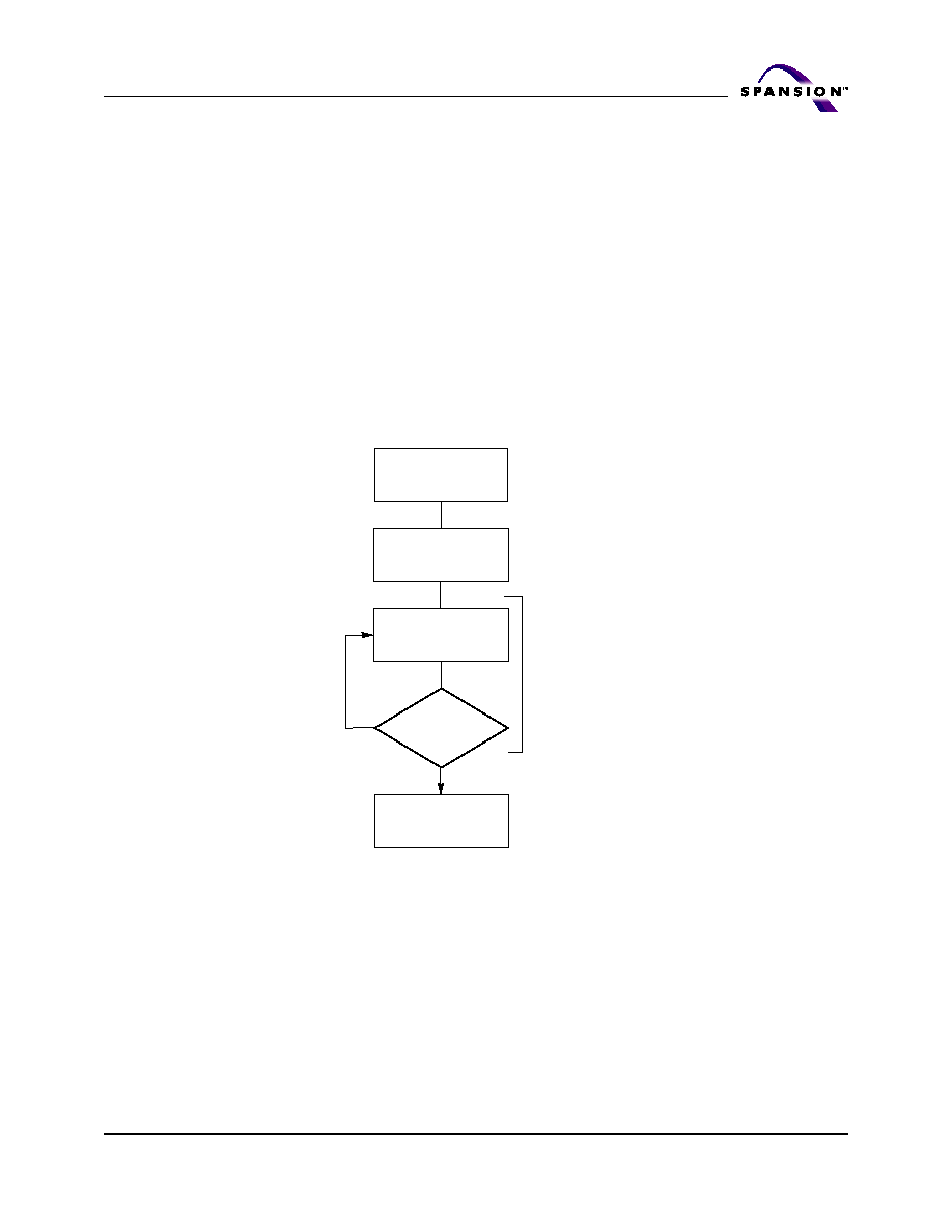
November 5, 2004 S29CD016_00_A4
S29CD016G
49
A d v a n c e I n f o r m a t i o n
Automatic sector erase operations begin on the rising edge of the WE# or CE#
pulse of the last sector erase command issued, and once the 80 µs time-out win-
dow expires. The status of the sector erase operation is determined three ways:
Data# polling of the DQ7 pin
Checking the status of the toggle bit DQ6
Checking the status of the RY/BY# pin
Further status of device activity during the sector erase operation is determined
using toggle bit DQ2 (refer to
"DQ2: Toggle Bit II" on page 63
).
When the Embedded Erase algorithm is complete, the device returns to reading
array data, and addresses are no longer latched. Note that an address change is
required to begin read valid array data.
Figure 5
illustrates the EmbeddedTM Erase Algorithm, using a typical command
sequence and bus operation. Refer to
Table 29 on page 85
for parameters, and
Figure 21, on page 78
and
Figure 22, on page 79
for timing diagrams.
Sector Erase and Program Suspend Command
The Sector Erase and Program Suspend command allows the user to interrupt a
Sector Erase or Program operation and perform data read or programs in a sector
that is not being erased or to the sector where a programming operation was ini-
tiated. This command is applicable only during the Sector Erase and
Programming operation, which includes the time-out period for Sector Erase.
START
Write Erase
Command Sequence
Data Poll
from System
Data = FFh?
No
Yes
Erasure Completed
Embedded
Erase
algorithm
in progress
Notes:
1. See
Table 27 on page 77
and
Table 28 on page 83
for erase command sequence.
2. See
"DQ3: Sector Erase Timer" on page 65r
for more information.
Figure 5. Erase Operation

50
S29CD016G
S29CD016_00_A4 November 5, 2004
A d v a n c e I n f o r m a t i o n
Sector Erase and Program Suspend Operation Mechanics
The Sector Erase and Program Suspend command is ignored if written during the
execution of the Chip Erase operation or Embedded Program Algorithm (but re-
sets the chip if written improperly during the command sequences). Writing the
Sector Erase and Program command during the Sector Erase time-out results in
immediate termination of the time-out period and suspension of the erase oper-
ation. Once in Erase Suspend, the device is available for reading (note that in the
Erase Suspend mode, the Reset command is not required for read operations and
is ignored) or program operations in sectors not being erased. Any other com-
mand written during the Erase Suspend mode is ignored, except for the Sector
Erase and Program Resume command. Writing the Erase and Program Resume
command resumes the sector erase operation. The bank address of the erase
suspended bank is required when writing this command
If the Sector Erase and Program Suspend command is written during a program-
ming operation, the device suspends programming operations and allows only
read operations in sectors not selected for programming. Further nesting of either
erase or programming operations is not permitted.
Table 18
summarizes permis-
sible operations during Erase and Program Suspend. (A busy sector is one that is
selected for programming or erasure.)
Table 18. Allowed Operations During Erase/Program Suspend
When the Sector Erase and Program Suspend command is written during a Sector
Erase operation, the chip takes between 0.1 µs and 20 µs to actually suspend the
operation and go into the erase suspended read mode (pseudo-read mode), at
which time the user can read or program from a sector that is not erase sus-
pended. Reading data in this mode is the same as reading from the standard read
mode, except that the data must be read from sectors that have not been erase
suspended.
Polling DQ6 on two immediately consecutive reads from a given address provides
the system with the ability to determine if the device is in Erase or Program Sus-
pend. Before the device enters Erase or Program Suspend, the DQ6 pin toggles
between two immediately consecutive reads from the same address. After the
device enters Erase suspend, DQ6 stops toggling between two immediately con-
secutive reads to the same address. During the Sector Erase operation and also
in Erase suspend mode, two immediately consecutive readings from the erase-
suspended sector causes DQ2 to toggle. DQ2 does not toggle if reading from a
non-busy (non-erasing) sector (stored data is read). No bits are toggled during
program suspend mode. Software must keep track of the fact that the device is
in a suspended mode.
After entering the erase-suspend-read mode, the system may read or program
within any non-suspended sector:
A read operation from the erase-suspended bank returns polling data up to
20 µs after the erase suspend command is issued; read operations thereafter
return array data. Read operations from the other bank return array data with
no latency.
Sector
Program Suspend
Erase Suspend
Busy Sector
Program Resume
Erase Resume
Non-busy
sectors
Read Only
Read or Program

November 5, 2004 S29CD016_00_A4
S29CD016G
51
A d v a n c e I n f o r m a t i o n
A program operation while in the erase suspend mode is the same as pro-
gramming in the regular program mode, except that the data must be pro-
grammed to a sector that is not erase suspended. Write operation status is
obtained in the same manner as a normal program operation.
Sector Erase and Program Resume Command
The Sector Erase and Program Resume command (30h) resumes a Sector Erase
or Program operation that was suspended. Any further writes of the Sector Erase
and Program Resume command ignored. However, another Sector Erase and Pro-
gram Suspend command can be written after the device resumes sector erase
operations. Note that until a suspended program or erase operation resumes, the
contents of that sector are unknown.
The Sector Erase and Program Resume Command is ignored if the SecSi sector
is enabled.
Configuration Register Read Command
The Configuration Register Read command is used to verify the contents of the
Configuration Register. Execution of this command is only allowed while in user
mode and is not available during Unlock Bypass mode or during Security mode.
The Configuration Register Read command is preceded by the standard two-cycle
"unlock" sequence, followed by the Configuration Register Read command (C6h),
and finally followed by performing a read operation to the bank address specified
when the C6h command was written. Reading the other bank results in reading
the flash memory contents. The contents of the Configuration Register are place
on DQ15≠DQ0. The contents of DQ31≠DQ16 are XXXXh and should be ignored.
The user should execute the Read/Reset command to place the device back in
standard user operation after executing the Configuration Register Read
command.
The Configuration Register Read Command is fully operational if the SecSi sector
is enabled.
Configuration Register Write Command
The Configuration Register Write command is used to modify the contents of the
Configuration Register. Execution of this command is only allowed while in user
mode and is not available during Unlock Bypass mode or during Security mode.
The Configuration Register Write command is preceded by the standard two-cycle
"unlock" sequence, followed by the Configuration Register Write command (D0h),
and finally followed by writing the contents of the Configuration Register to any
address. The contents of the Configuration Register are place on DQ31≠DQ0. The
contents of DQ31≠DQ16 are XXXXh and are ignored. Writing the Configuration
Register while an Embedded AlgorithmTM or Erase Suspend modes are executing
results in the contents of the Configuration Register not being updated.
The Configuration Register Read Command is fully operational if the SecSi sector
is enabled.
Common Flash Interface (CFI) Command
The Common Flash Interface (CFI) command provides device size, geometry, and
capability information directly to the users system. Flash devices that support
CFI, have a "Query Command" that returns information about the device to the
system. The Query structure contents are read at the specific address locations
following a single system write cycle where:

52
S29CD016G
S29CD016_00_A4 November 5, 2004
A d v a n c e I n f o r m a t i o n
A 98h query command code is written to 55h address location within the de-
vice's address space
The device is initially in any valid read state, such as "Read Array" or "Read
ID Data"
Other device statistics may exist within a long sequence of commands or data in-
put; such sequences must first be completed or terminated before writing of the
98H Query command, otherwise invalid Query data structure output may result.
Note that for data bus bits greater than DQ7 (DQ31≠DQ8), the valid Query access
code contains all zeroes ("0"s) in the upper DQ bus locations. Thus, the 16-bit
Query command code is 0098h and the 32-bit Query command code is
00000098h.
To terminate the CFI operation, it is necessary to execute the Read/Reset
command.
The CFI command is not permitted if the SecSi sector is enabled and Simulta-
neous Read/Write operation is disabled once the command is entered.
See
"Common Flash Interface (CFI) Command" on page 51
for the specific CFI
command codes.
SecSi Sector Entry Command
The SecSi Sector Entry command enables the SecSi (OTP) sector to overlay the
8 KB outermost sector in the small (25%) bank. The SecSi sector overlays
00000h≠0003Fh for the top bootblock configuration and 7FFC0h≠7FFFFh for the
bottom bootblock configuration. Address range 00040h≠007FFh for the top boot-
block and 7F800h≠7FFBFh return invalid data when addressed with the SecSi
sector enabled. The following commands are permitted after issuing the SecSi
Sector Entry command:
1.
Autoselect
2.
Password Program
3.
Password Verify
4.
Password Unlock
5.
Read/Reset
6.
Program
7.
Chip and Sector Erase
8.
SecSi Sector Protection Bit Program
9.
PPB Program
10.
All PPB Erase
11.
PPB Lock Bit Set
12.
DYB Write
13.
DYB/PPB/PPB Lock Bit Verify
14.
Security Reset
15.
Configuration Register Write
16.
Configuration Register Read
The following commands are unavailable when the SecSi sector is enabled. Issu-
ing the following commands while the SecSi sector is enabled results in the
command being ignored.
1.
Unlock Bypass
2.
CFI
3.
Accelerated Program

November 5, 2004 S29CD016_00_A4
S29CD016G
53
A d v a n c e I n f o r m a t i o n
4.
Program and Sector Erase Suspend
5.
Program and Sector Erase Resume
The SecSi Sector Entry command is allowed when the device is in either program
or erase suspend modes. If the SecSi sector is enabled, the program or erase sus-
pend command is ignored. This prevents resuming either programming or
erasure on the SecSi sector if the overlayed sector was undergoing programming
or erasure. The host system must ensure that the device resume any sus-
pended program or erase operation after exiting the SecSi sector.
Executing any of the PPB program/erase commands, or Password Unlock com-
mand results in the small bank (25% bank) returning the status of these
operations while they are in progress, thus making the SecSi sector unavailable
for reading. If the SecSi sector is enabled while the DYB command is issued, the
DYB for the overlayed sector is NOT updated. Reading the DYB status using the
PPB Lock Bit/DYBDYB verify command when the SecSi sector is enabled returns
invalid data.
Password Program Command
The Password Program Command permits programming the password that is
used as part of the hardware protection scheme. The actual password is 64-bits
long. Depending upon the state of the WORD# pin, multiple Password Program
Commands are required. For a x32 bit data bus, 2 Password Program commands
are required. The user must enter the unlock cycle, password program command
(38h) and the program address/data for each portion of the password when pro-
gramming. There are no provisions for entering the 2-cycle unlock cycle, the
password program command, and all the password data. There is no special ad-
dressing order required for programming the password. Also, when the password
is undergoing programming, Simultaneous Read/Write operation is disabled.
Read operations to any memory location returns the programming status. Once
programming is complete, the user must issue a Read/Reset command to return
the device to normal operation. Once the Password is written and verified, the
Password Mode Locking Bit must be set in order to prevent verification. The Pass-
word Program Command is only capable of programming "0"s. Programming a
"1" after a cell is programmed as a "0" results in a time-out by the Embedded
Program AlgorithmTM with the cell remaining as a "0". The password is all F's when
shipped from the factory. All 64-bit password combinations are valid as a
password.
Password Programming is permitted if the SecSi sector is enabled.
Password Verify Command
The Password Verify Command is used to verify the Password. The Password is
verifiable only when the Password Mode Locking Bit is not programmed. If the
Password Mode Locking Bit is programmed and the user attempts to verify the
Password, the device always drives all F's onto the DQ data bus.
The Password Verify command is permitted if the SecSi sector is enabled. Also,
Simultaneous Read/Write operation is disabled when the Password Verify com-
mand is executed. Only the password is returned regardless of the bank address.
The lower two address bits (A0:A-1) are valid during the Password Verify. Writing
the Read/Reset command returns the device back to normal operation.

54
S29CD016G
S29CD016_00_A4 November 5, 2004
A d v a n c e I n f o r m a t i o n
Password Protection Mode Locking Bit Program Command
The Password Protection Mode Locking Bit Program Command programs the
Password Protection Mode Locking Bit, which prevents further verifies or updates
to the Password. Once programmed, the Password Protection Mode Locking Bit
cannot be erased! If the Password Protection Mode Locking Bit is verified as pro-
gram without margin, the Password Protection Mode Locking Bit Program
command can be executed to improve the program margin. Once the Password
Protection Mode Locking Bit is programmed, the Persistent Sector Protection
Locking Bit program circuitry is disabled, thereby forcing the device to remain in
the Password Protection mode. Exiting the Mode Locking Bit Program command
is accomplished by writing the Read/Reset command.
The Password Protection Mode Locking Bit Program command is permitted if the
SecSi sector is enabled.
Persistent Sector Protection Mode Locking Bit Program Command
The Persistent Sector Protection Mode Locking Bit Program Command programs
the Persistent Sector Protection Mode Locking Bit, which prevents the Password
Mode Locking Bit from ever being programmed. If the Persistent Sector Protec-
tion Mode Locking Bit is verified as programmed without margin, the Persistent
Sector Protection Mode Locking Bit Program Command should be reissued to im-
prove program margin. By disabling the program circuitry of the Password Mode
Locking Bit, the device is forced to remain in the Persistent Sector Protection
mode of operation, once this bit is set. Exiting the Persistent Protection Mode
Locking Bit Program command is accomplished by writing the Read/Reset
command.
The Persistent Sector Protection Mode Locking Bit Program command is permitted
if the SecSi sector is enabled.
SecSi Sector Protection Bit Program Command
The SecSi Sector Protection Bit Program Command programs the SecSi Sector
Protection Bit, which prevents the SecSi sector memory from being cleared. If the
SecSi Sector Protection Bit is verified as programmed without margin, the SecSi
Sector Protection Bit Program Command should be reissued to improve program
margin. Exiting the V
CC
-level SecSi Sector Protection Bit Program Command is
accomplished by writing the Read/Reset command.
The SecSi Sector Protection Bit Program command is permitted if the SecSi sector
is enabled.
PPB Lock Bit Set Command
The PPB Lock Bit Set command is used to set the PPB Lock bit if it is cleared either
at reset or if the Password Unlock command was successfully executed. There is
no PPB Lock Bit Clear command. Once the PPB Lock Bit is set, it cannot be cleared
unless the device is taken through a power-on clear or the Password Unlock com-
mand is executed. Upon setting the PPB Lock Bit, the PPBs are latched into the
DYBs. If the Password Mode Locking Bit is set, the PPB Lock Bit status is reflected
as set, even after a power-on reset cycle. Exiting the PPB Lock Bit Set command
is accomplished by writing the Read/Reset command.
The PPB Lock Bit Set command is permitted if the SecSi sector is enabled.

November 5, 2004 S29CD016_00_A4
S29CD016G
55
A d v a n c e I n f o r m a t i o n
DYB Write Command
The DYB Write command is used to set or clear a DYB for a given sector. The high
order address bits (A18≠A11) are issued at the same time as the code 01h or 00h
on DQ7-DQ0. All other DQ data bus pins are ignored during the data write cycle.
The DYBs are modifiable at any time, regardless of the state of the PPB or PPB
Lock Bit. The DYBs are cleared at power-up or hardware reset.Exiting the DYB
Write command is accomplished by writing the Read/Reset command.
The DYB Write command is permitted if the SecSi sector is enabled.
Password Unlock Command
The Password Unlock command is used to clear the PPB Lock Bit so that the PPBs
can be unlocked for modification, thereby allowing the PPBs to become accessible
for modification. The exact password must be entered in order for the unlocking
function to occur. This command cannot be issued any faster than 2 µs at a time
to prevent a hacker from running through the all 64-bit combinations in an at-
tempt to correctly match a password. If the command is issued before the 2 µs
execution window for each portion of the unlock, the command is ignored.
The Password Unlock function is accomplished by writing Password Unlock com-
mand and data to the device to perform the clearing of the PPB Lock Bit. The
password is 64 bits long, so the user must write the Password Unlock command
2 times for a x32 bit data bus. A0 is used to determine whether the 32 bit data
quantity is used to match the upper 32 bits or lower 32 bits. Writing the Password
Unlock command is address order specific. In other words, for the x32 data bus
configuration, the lower 32 bits of the password are written first and then the
upper 32 bits of the password are written. Writing out of sequence results in the
Password Unlock not returning a match with the password and the PPB Lock Bit
remains set.
Once the Password Unlock command is entered, the RY/BY# pin goes LOW indi-
cating that the device is busy. Also, reading the small bank (25% bank) results
in the DQ6 pin toggling, indicating that the Password Unlock function is in
progress. Reading the large bank (75% bank) returns actual array data. Approx-
imately 1uSec is required for each portion of the unlock. Once the first portion of
the password unlock completes (RY/BY# is not driven and DQ6 does not toggle
when read), the Password Unlock command is issued again, only this time with
the next part of the password. The second Password Unlock command is the final
command before the PPB Lock Bit is cleared (assuming a valid password). As with
the first Password Unlock command, the RY/BY# signal goes LOW and reading
the device results in the DQ6 pin toggling on successive read operations until
complete. It is the responsibility of the microprocessor to keep track of the num-
ber of Password Unlock commands (2 for x32 bus), the order, and when to read
the PPB Lock bit to confirm successful password unlock
The Password Unlock command is permitted if the SecSi sector is enabled.
PPB Program Command
The PPB Program command is used to program, or set, a given PPB. Each PPB is
individually programmed (but is bulk erased with the other PPBs). The specific
sector address (A18≠A11) are written at the same time as the program command
60h with A6 = 0. If the PPB Lock Bit is set and the corresponding PPB is set for
the sector, the PPB Program command does not execute and the command times
out without programming the PPB.

56
S29CD016G
S29CD016_00_A4 November 5, 2004
A d v a n c e I n f o r m a t i o n
The host system must determine whether a PPB was fully programmed by noting
the status of DQ0 in the sixth cycle of the PPB Program command. If DQ0 = 0,
the entire six-cycle PPB Program command sequence must be reissued until DQ0
= 1.
All PPB Erase Command
The All PPB Erase command is used to erase all PPBs in bulk. There is no means
for individually erasing a specific PPB. Unlike the PPB program, no specific sector
address is required. However, when the PPB erase command is written (60h) and
A6 = 1, all Sector PPBs are erased in parallel. If the PPB Lock Bit is set the ALL
PPB Erase command does not execute and the command times out without eras-
ing the PPBs. The host system must determine whether all PPB was fully erased
by noting the status of DQ0 in the sixth cycle of the All PPB Erase command. If
DQ0 = 1, the entire six-cycle All PPB Erase command sequence must be reissued
until DQ0 = 1.
It is the responsibility of the user to preprogram all PPBs prior to issuing the All
PPB Erase command. If the user attempts to erase a cleared PPB, over-erasure
may occur making it difficult to program the PPB at a later time. Also note that
the total number of PPB program/erase cycles is limited to 100 cycles. Cycling the
PPBs beyond 100 cycles is not guaranteed.
The All PPB Erase command is permitted if the SecSi sector is enabled.
DYB Write
The DYB Write command is used for setting the DYB, which is a volatile bit that
is cleared at reset. There is one DYB per sector. If the PPB is set, the sector is
protected regardless of the value of the DYB. If the PPB is cleared, setting the
DYB to a 1 protects the sector from programs or erases. Since this is a volatile
bit, removing power or resetting the device clears the DYBs. The bank address is
latched when the command is written.
The DYB Write command is permitted if the SecSi sector is enabled.
PPB Lock Bit Set
The PPB Lock Bit set command is used for setting the DYB, which is a volatile bit
that is cleared at reset. There is one DYB per sector. If the PPB is set, the sector
is protected regardless of the value of the DYB. If the PPB is cleared, setting the
DYB to a 1 protects the sector from programs or erases. Since this is a volatile
bit, removing power or resetting the device clears the DYBs. The bank address is
latched when the command is written.
The PPB Lock command is permitted if the SecSi sector is enabled.
DYB Status
The programming of the DYB for a given sector can be verified by writing a DYB
status verify command to the device.
PPB Status
The programming of the PPB for a given sector can be verified by writing a PPB
status verify command to the device.
PPB Lock Bit Status
The programming of the PPB Lock Bit for a given sector can be verified by writing
a PPB Lock Bit status verify command to the device.

November 5, 2004 S29CD016_00_A4
S29CD016G
57
A d v a n c e I n f o r m a t i o n
Non-volatile Protection Bit Program And Erase Flow
The device uses a standard command sequence for programming or erasing the
SecSi Sector Protection, Password Locking, Persistent Sector Protection Mode
Locking, or Persistent Protection Bits. Unlike devices that have the Single High
Voltage Sector Unprotect/Protect feature, the device has the standard two-cycle
unlock followed by 60h, which places the device into non-volatile bit program or
erase mode. Once the mode is entered, the specific non-volatile bit status is read
on DQ0. 1 shows a typical flow for programming the non-volatile bit and 2 shows
a typical flow for erasing the non-volatile bits. The SecSi Sector Protection, Pass-
word Locking, Persistent Sector Protection Mode Locking bits are not erasable
after they are programmed. However, the PPBs are both erasable and program-
mable (depending upon device security).
Unlike Single High Voltage Sector Protect/Unprotect, the A6 pin no longer func-
tions as the program/erase selector nor the program/erase margin enable.
Instead, this function is accomplished by issuing the specific command for either
program (68h) or erase (60h).
In asynchronous mode, the DQ6 toggle bit indicates whether the program or
erase sequence is active. (In synchronous mode, ADV# indicates the status.) If
the DQ6 toggle bit toggles with either OE# or CE#, the non-volatile bit program
or erase operation is in progress. When DQ6 stops toggling, the value of the non-
volatile bit is available on DQ0.
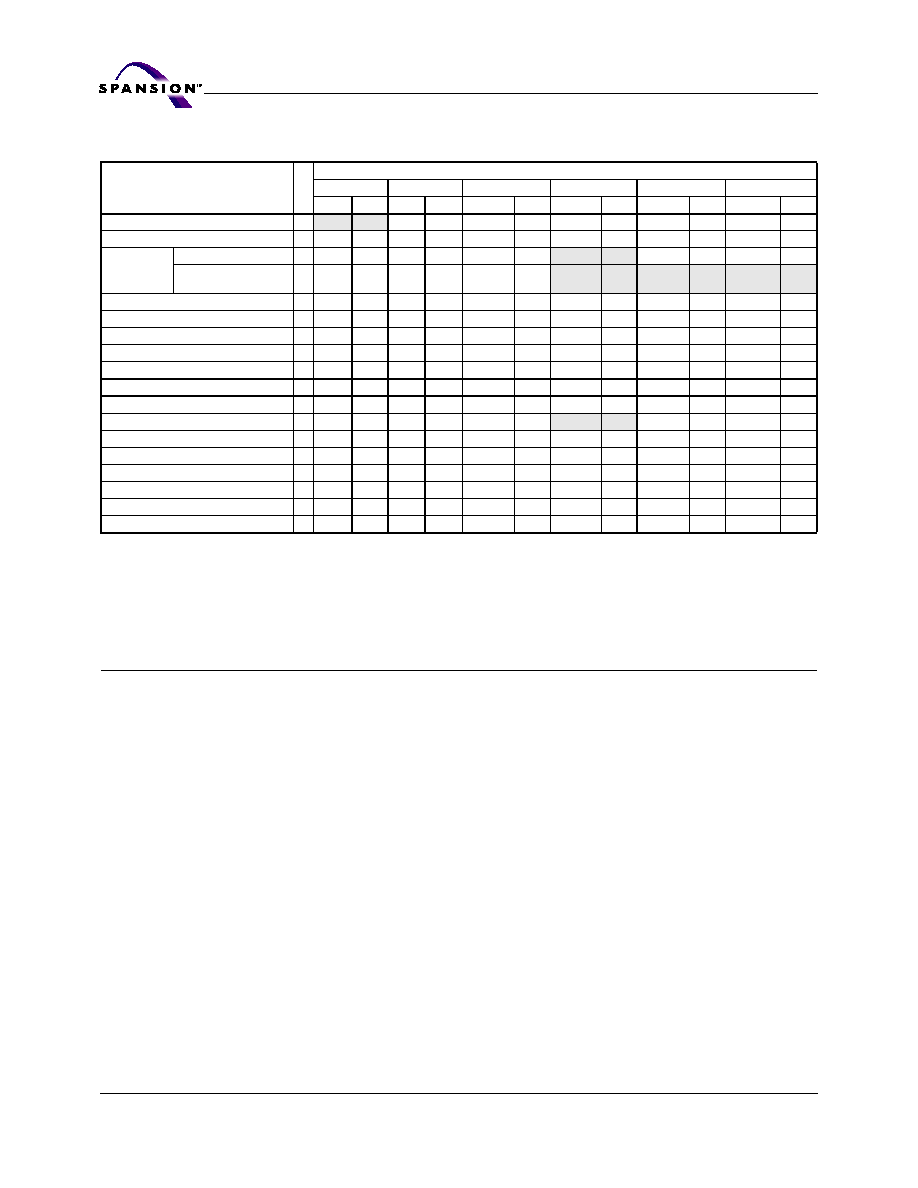
58
S29CD016G
S29CD016_00_A4 November 5, 2004
A d v a n c e I n f o r m a t i o n
Table 19. Memory Array Command Definitions (x32 Mode)
Command (Notes)
Cyc
l
e
s
Bus Cycles (Notes 1≠4)
First
Second
Third
Fourth
Fifth
Sixth
Addr Data Addr Data
Addr
Data
Addr
Data
Addr
Data
Addr
Data
Read (5)
1
RA
RD
Reset (6)
1
XXX
F0
Autoselect
(7)
Manufacturer ID
4
555
AA
2AA
55
555
90
BA+X00
01
Device ID (11)
6
555
AA
2AA
55
555
90
BA+X01
7E
BA+X0E
36
BA+X0F
00/
01
Program
4
555
AA
2AA
55
555
A0
PA
PD
Chip Erase
6
555
AA
2AA
55
555
80
555
AA
2AA
55
555
10
Sector Erase
6
555
AA
2AA
55
555
80
555
AA
2AA
55
SA
30
Program/Erase Suspend (12)
1
BA
B0
Program/Erase Resume (13)
1
BA
30
CFI Query (14, 15)
1
55
98
Accelerated Program (16)
2
XX
A0
PA
PD
Configuration Register Verify (15)
3
555
AA
2AA
55
BA+555
C6
BA+XX
RD
Configuration Register Write (17)
4
555
AA
2AA
55
555
D0
XX
WD
Unlock Bypass Entry (18)
3
555
AA
2AA
55
555
20
Unlock Bypass Program (18)
2
XX
A0
PA
PD
Unlock Bypass Erase (18)
2
XX
80
XX
10
Unlock Bypass CFI (14, 18)
1
XX
98
Unlock Bypass Reset (18)
2
XX
90
XX
00
Legend:
BA = Address of the bank that is being switched to autoselect mode,
is in bypass mode, or is being erased. Determined by A18 and A17,
see Tables 11 and 12 for more detail.
PA = Program Address (A18:A0). Addresses latch on the falling edge
of the WE# or CE# pulse, whichever happens later.
PD = Program Data (DQ31:DQ0) written to location PA. Data latches
on the rising edge of WE# or CE# pulse, whichever happens first.
RA = Read Address (A18:A0).
RD = Read Data (DQ31:DQ0) from location RA.
SA = Sector Address (A18:A11) for verifying (in autoselect mode),
erasing, or applying security commands.
WD = Write Data. See "Configuration Register" definition for specific
write data. Data latched on rising edge of WE#.
X = Don't care
Notes:
1. See
Table 1 on page 14
for description of bus operations.
2. All values are in hexadecimal.
3. Shaded cells in table denote read cycles. All other cycles are
write operations.
4. During unlock cycles, (lower address bits are 555 or 2AAh as
shown in table) address bits higher than A11 (except where BA
is required) and data bits higher than DQ7 are don't cares.
5. No unlock or command cycles required when bank is reading
array data.
6. The Reset command is required to return to the read mode (or
to the erase-suspend-read mode if previously in Erase Suspend)
when a bank is in the autoselect mode, or if DQ5 goes high
(while the bank is providing status information).
7. The fourth cycle of the autoselect command sequence is a read
cycle. The system must provide the bank address to obtain the
manufacturer ID or device ID information. See the
"Autoselect
Command" on page 44
section for more information.
8. This command cannot be executed until The Unlock Bypass
command must be executed before writing this command
sequence. The Unlock Bypass Reset command must be executed
to return to normal operation.
9. This command is ignored during any embedded program, erase
or suspended operation.
10. Valid read operations include asynchronous and burst read mode
operations.
11. The device ID must be read across the fourth, fifth, and sixth
cycles. 00h in the sixth cycle indicates ordering option 00, 01h
indicates ordering option 01.
12. The system may read and program in non-erasing sectors, or
enter the autoselect mode, when in the Program/Erase Suspend
mode. The Program/Erase Suspend command is valid only
during a sector erase operation, and requires the bank address.
13. The Program/Erase Resume command is valid only during the
Erase Suspend mode, and requires the bank address.
14. Command is valid when device is ready to read array data or
when device is in autoselect mode.
15. Asynchronous read operations.
16. ACC must be at V
ID
during the entire operation of this command.
17. Command is ignored during any Embedded Program, Embedded
Erase, or Suspend operation.
18. The Unlock Bypass Entry command is required prior to any
Unlock Bypass operation. The Unlock Bypass Reset command is
required to return to the read mode.
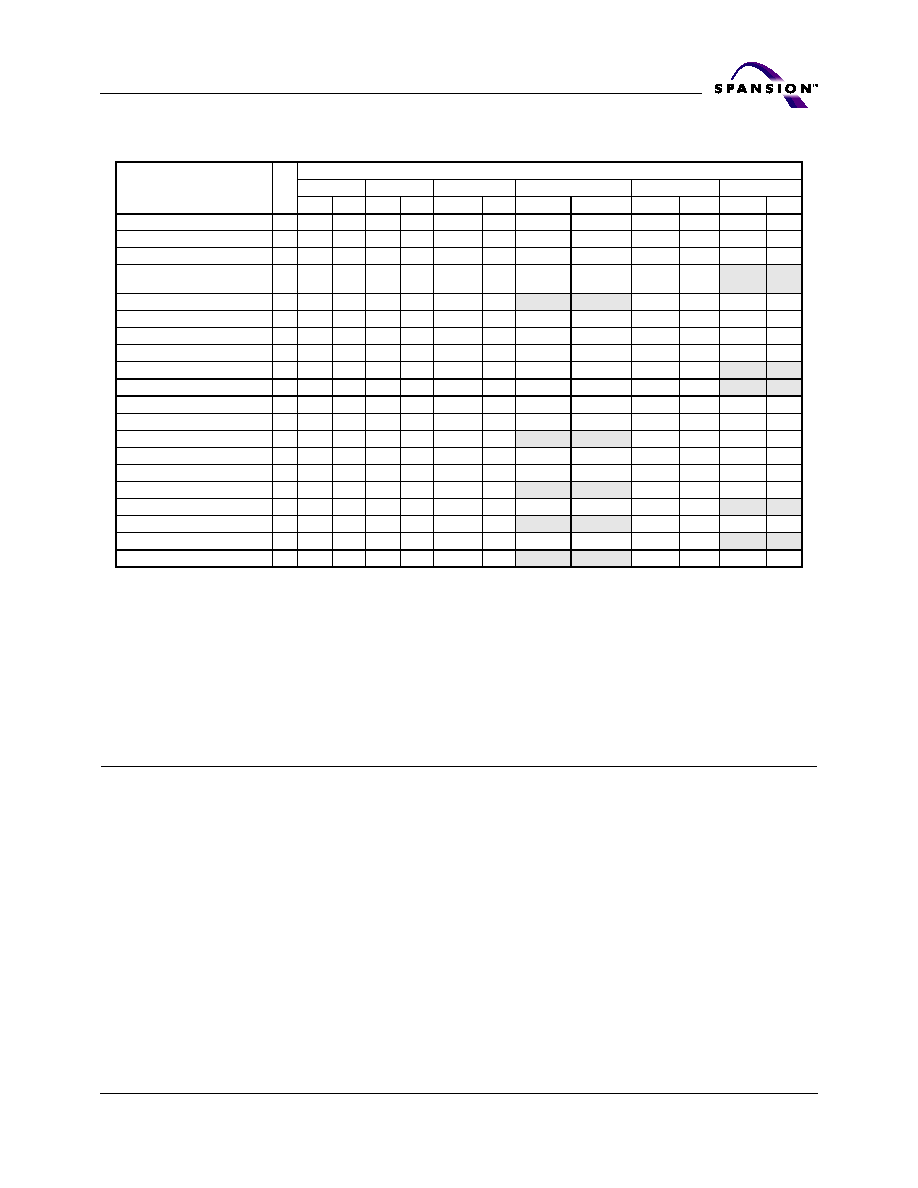
November 5, 2004 S29CD016_00_A4
S29CD016G
59
A d v a n c e I n f o r m a t i o n
Table 20. Sector Protection Command Definitions (x32 Mode)
Command (Notes)
Cyc
l
e
s
Bus Cycles (Notes 1-4)
First
Second
Third
Fourth
Fifth
Sixth
Addr Data Addr Data
Addr
Data
Addr
Data
Addr
Data
Addr
Data
Reset
1
XXX
F0
SecSi Sector Entry
3
555
AA
2AA
55
555
88
SecSi Sector Exit
4
555
AA
2AA
55
555
90
XX
00
SecSi Protection Bit Program
(5, 6)
6
555
AA
2AA
55
555
60
OW
68
OW
48
OW
RD(0)
SecSi Protection Bit Status
6
555
AA
2AA
55
555
60
OW
RD(0)
Password Program (5, 7, 8)
4
555
AA
2AA
55
555
38
PWA[0-1] PWD[0-1]
Password Verify
4
555
AA
2AA
55
555
C8
PWA[0-1] PWD[0-1]
Password Unlock (7, 8)
5
555
AA
2AA
55
555
28
PWA[0-1] PWD[0-1]
PPB Program (5, 6)
6
555
AA
2AA
55
555
60
SG+WP
68
SG+WP
48
SG+WP RD(0)
All PPB Erase (5, 9, 10)
6
555
AA
2AA
55
555
60
WP
60
WP
40
WP
RD(0)
PPB Status (11, 12)
4
555
AA
2AA
55
SG+555
90
SA+X02
00/01
PPB Lock Bit Set
3
555
AA
2AA
55
555
78
PPB Lock Bit Status
4
555
AA
2AA
55
555
58
SA
RD(1)
DYB Write (7)
4
555
AA
2AA
55
555
48
SA
X1
DYB Erase (7)
4
555
AA
2AA
55
555
48
SA
X0
DYB Status (12)
4
555
AA
2AA
55
SA+555
58
SA
RD(0)
PPMLB Program (5,6)
6
555
AA
2AA
55
555
60
PL
68
PL
48
PL
RD(0)
PPMLB Status (5)
6
555
AA
2AA
55
555
60
PL
RD(0)
SPMLB Program (5, 6)
6
555
AA
2AA
55
555
60
SL
68
SL
48
SL
RD(0)
SPMLB Status (5)
6
555
AA
2AA
55
555
60
SL
RD(0)
Legend:
DYB = Dynamic Protection Bit
OW = Address (A5≠A0) is (011X10).
PPB = Persistent Protection Bit
PWA = Password Address. A0 selects between the low and high 32-bit
portions of the 64-bit Password
PWD = Password Data. Must be written over two cycles.
PL = Password Protection Mode Lock Address (A5≠A0) is (001X10)
RD(0) = Read Data DQ0 protection indicator bit. If protected, DQ0=
1, if unprotected, DQ0 = 0.
RD(1) = Read Data DQ1 protection indicator bit. If protected, DQ1 =
1, if unprotected, DQ1 = 0.
SA = Sector Address where security command applies. Address bits
A18:A11 uniquely select any sector.
SG = Sector Group Address
BA = Bank Address
SL = Persistent Protection Mode Lock Address (A5≠A0) is (010X10)
WP = PPB Address (A5≠A0) is (111010)
X = Don't care
PPMLB = Password Protection Mode Locking Bit
SPMLB = Persistent Protection Mode Locking Bit
Notes:
1. See
Table 1 on page 14
for description of bus operations.
2. All values are in hexadecimal.
3. Shaded cells in table denote read cycles. All other cycles are
write operations.
4. During unlock cycles, (lower address bits are 555 or 2AAh as
shown in table) address bits higher than A11 (except where BA
is required) and data bits higher than DQ7 are don't cares.
5. The reset command returns the device to reading the array.
6. The fourth cycle programs the addressed locking bit. The fifth
and sixth cycles are used to validate whether the bit was fully
programmed. If DQ0 (in the sixth cycle) reads 0, the program
command must be issued and verified again.
7. Data is latched on the rising edge of WE#.
8. The entire four bus-cycle sequence must be entered for each
portion of the password.
9. The fourth cycle erases all PPBs. The fifth and sixth cycles are
used to validate whether the bits were fully erased. If DQ0 (in
the sixth cycle) reads 1, the erase command must be issued and
verified again.
10. Before issuing the erase command, all PPBs should be
programmed in order to prevent over-erasure of PPBs.
11. In the fourth cycle, 00h indicates PPB set; 01h indicates PPB not
set.
12. The status of additional PPBs and DYBs may be read (following
the fourth cycle) without reissuing the entire command
sequence.

60
S29CD016G
S29CD016_00_A4 November 5, 2004
A d v a n c e I n f o r m a t i o n
Write Operation Status
The device provides several bits to determine the status of a write operation:
DQ2, DQ3, DQ5, DQ6, DQ7, and RY/BY#.
Table 21 on page 65
and the following
subsections describe the functions of these bits. DQ7, RY/BY#, and DQ6 each
offer a method for determining whether a program or erase operation is complete
or in progress. These three bits are discussed first.
DQ7: Data# Polling
The device features a Data# polling flag as a method to indicate to the host sys-
tem whether the embedded algorithms are in progress or are complete. During
the Embedded Program Algorithm an attempt to read the bank in which program-
ming was initiated produces the complement of the data last written to DQ7.
Upon completion of the Embedded Program Algorithm, an attempt to read the de-
vice produces the true last data written to DQ7. Note that DATA# polling returns
invalid data for the address being programmed or erased.
For example, the data read for an address programmed as 0000 0000 1000
0000b returns XXXX XXXX 0XXX XXXXb during an Embedded Program operation.
Once the Embedded Program Algorithm is complete, the true data is read back
on DQ7. Note that at the instant when DQ7 switches to true data, the other bits
may not yet be true. However, they will all be true data on the next read from the
device. Please note that Data# polling may give misleading status when an at-
tempt is made to write to a protected sector.
For chip erase, the Data# polling flag is valid after the rising edge of the sixth
WE# pulse in the six write pulse sequence. For sector erase, the Data# polling is
valid after the last rising edge of the sector erase WE# pulse. Data# polling must
be performed at sector addresses within any of the sectors being erased and not
a sector that is a protected sector. Otherwise, the status may not be valid. DQ7
= 0 during an Embedded Erase Algorithm (chip erase or sector erase operation)
but returns a "1" after the operation completes because it drops back into read
mode.
In asynchronous mode, just prior to the completion of the Embedded Algorithm
operations, DQ7 may change asynchronously while OE# is asserted low. (In syn-
chronous mode, ADV# exhibits this behavior.) The status information may be
invalid during the instance of transition from status information to array (mem-
ory) data. An extra validity check is therefore specified in the data polling
algorithm. The valid array data on DQ31≠DQ0 is available for reading on the next
successive read attempt.
The Data# polling feature is only active during the Embedded Programming Al-
gorithm, Embedded Erase Algorithm, Erase Suspend, Erase Suspend-Program
mode, or sector erase time-out.
If the user attempts to write to a protected sector, Data# polling is activated for
about 1 µs: the device then returns to read mode, with the data from the pro-
tected sector unchanged. If the user attempts to erase a protected sector, Toggle
Bit (DQ6) is activated for about 150 µs; the device then returns to read mode,
without having erased the protected sector.
Table 21 on page 65
shows the outputs for Data# Polling on DQ7.
Figure 6, on
page 61
shows the Data# Polling algorithm.
Figure 24, on page 80
shows the
timing diagram for synchronous status DQ7 data polling.
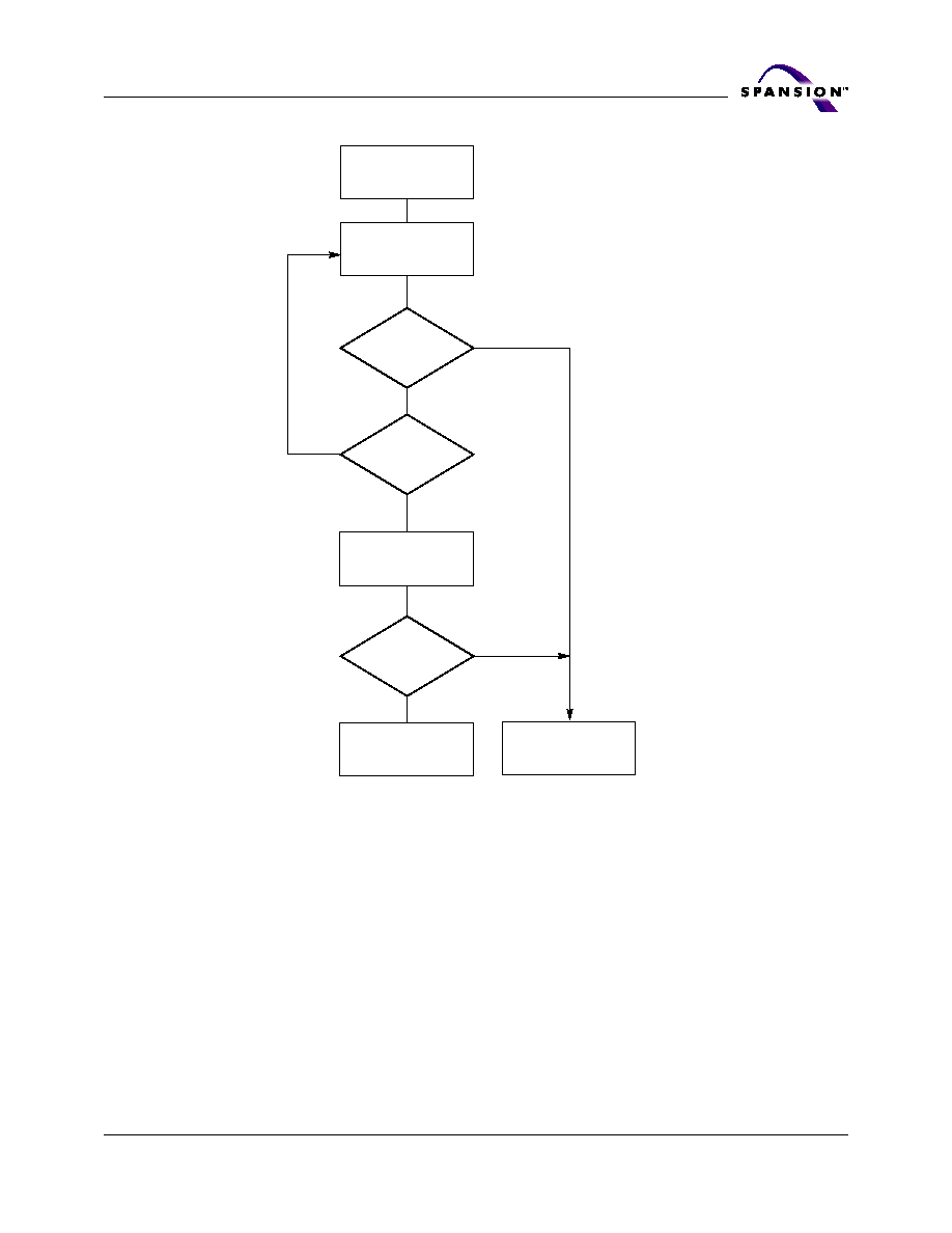
November 5, 2004 S29CD016_00_A4
S29CD016G
61
A d v a n c e I n f o r m a t i o n
DQ7 = Data?
Yes
No
No
DQ5 = 1?
No
Yes
Yes
FAIL
PASS
Read DQ7≠DQ0
Addr = VA
Read DQ7≠DQ0
Addr = VA
DQ7 = Data?
START
Notes:
1. VA = Valid address for programming. During a sector erase operation, a valid address is an address within any sector
selected for erasure. During chip erase, a valid address is any non-protected sector address.
2. DQ7 should be rechecked even if DQ5 = "1" because DQ7 may change simultaneously with DQ5.
Figure 6. Data# Polling Algorithm

62
S29CD016G
S29CD016_00_A4 November 5, 2004
A d v a n c e I n f o r m a t i o n
RY/BY#: Ready/Busy#
The device provides a RY/BY# open drain output pin as a way to indicate to the
host system that the Embedded Algorithms are either in progress or are com-
pleted. If the output is low, the device is busy with either a program, erase, or
reset operation. If the output is floating, the device is ready to accept any read/
write or erase operation. When the RY/BY# pin is low, the device does not accept
any additional program or erase commands with the exception of the Erase sus-
pend command. If the device enters Erase Suspend mode, the RY/BY# output is
floating. For programming, the RY/BY# is valid (RY/BY# = 0) after the rising edge
of the fourth WE# pulse in the four write pulse sequence. For chip erase, the RY/
BY# is valid after the rising edge of the sixth WE# pulse in the six write pulse
sequence. For sector erase, the RY/BY# is also valid after the rising edge of the
sixth WE# pulse.
If RESET# is asserted during a program or erase operation, the RY/BY# pin re-
mains a "0" (busy) until the internal reset operation is complete, which requires
a time of t
READY
(during Embedded Algorithms). The system can thus monitor RY/
BY# to determine whether the reset operation is complete. If RESET# is asserted
when a program or erase operation is not executing (RY/BY# pin is "floating"),
the reset operation is completed in a time of t
READY
(not during Embedded Algo-
rithms). The system can read data t
RH
after the RESET# pin returns to V
IH
.
Since the RY/BY# pin is an open-drain output, several RY/BY# pins can be tied
together in parallel with a pull-up resistor to V
CC
. An external pull-up resistor is
required to take RY/BY# to a V
IH
level since the output is an open drain.
Table 21 on page 65
shows the outputs for RY/BY#.
Figure 16, on page 73
,
Figure 19, on page 75
,
Figure 21, on page 78
and
Figure 23, on page 79
shows
RY/BY# for read, reset, program, and erase operations, respectively.
DQ6: Toggle Bit I
Toggle Bit I on DQ6 indicates whether an Embedded Program or Erase algorithm
is in progress or completed, or whether the device entered the Erase Suspend
mode. Toggle Bit I may be read at any address, and is valid after the rising edge
of the final WE# pulse in the command sequence (prior to the program or erase
operation), and during the sector erase time-out.
During an Embedded Program or Erase algorithm operation, two immediately
consecutive read cycles to any address cause DQ6 to toggle. When the operation
is complete, DQ6 stops toggling. For asynchronous mode, either OE# or CE# can
be used to control the read cycles. For synchronous mode, the rising edge of
ADV# is used or the rising edge of clock while ADV# is Low.
After an erase command sequence is written, if all sectors selected for erasing
are protected, DQ6 toggles for approximately 100 µs, then returns to reading
array data. If not all selected sectors are protected, the Embedded Erase algo-
rithm erases the unprotected sectors, and ignores the selected sectors that are
protected.
The system can use DQ6 and DQ2 together to determine whether a sector is ac-
tively erasing or is erase-suspended. When the device is actively erasing (that is,
the Embedded Erase algorithm is in progress), DQ6 toggles. When the device en-
ters the Erase Suspend mode, DQ6 stops toggling. However, the system must
also use DQ2 to determine which sectors are erasing or erase-suspended. Alter-
natively, the system can use DQ7 (see the subsection on
"DQ7: Data# Polling"
on page 60
).

November 5, 2004 S29CD016_00_A4
S29CD016G
63
A d v a n c e I n f o r m a t i o n
If a program address falls within a protected sector, DQ6 toggles for approxi-
mately 1 µs after the program command sequence is written, then returns to
reading array data.
DQ6 also toggles during the erase-suspend-program mode, and stops toggling
once the Embedded Program algorithm is complete.
Table 21 on page 65
shows the outputs for Toggle Bit I on DQ6.
Figure 7, on
page 64
shows the toggle bit algorithm in flowchart form, and the section
"Read-
ing Toggle Bits DQ6/DQ2" on page 63
explains the algorithm.
Figure 25, on
page 80
shows the toggle bit timing diagrams.
Figure 25, on page 80
shows the
differences between DQ2 and DQ6 in graphical form. See also the subsection on
"DQ2: Toggle Bit II"
.
Figure 25, on page 80
shows the timing diagram for syn-
chronous toggle bit status.
DQ2: Toggle Bit II
The "Toggle Bit II" on DQ2, when used with DQ6, indicates whether a particular
sector is actively erasing (that is, the Embedded Erase algorithm is in progress),
or whether that sector is erase-suspended. Toggle Bit II is valid after the rising
edge of the final WE# pulse in the command sequence.
DQ2 toggles when the system performs two immediately consecutive reads at
addresses within those sectors that were selected for erasure. (For asynchronous
mode, either OE# or CE# can be used to control the read cycles. For synchronous
mode, ADV# is used.) But DQ2 cannot distinguish whether the sector is actively
erasing or is erase-suspended. DQ6, by comparison, indicates whether the device
is actively erasing, or is in Erase Suspend, but cannot distinguish which sectors
are selected for erasure. Thus, both status bits are required for sector and mode
information. Refer to
Table 21 on page 65
to compare outputs for DQ2 and DQ6.
Figure 7, on page 64
shows the toggle bit algorithm in flowchart form, and the
section
"Reading Toggle Bits DQ6/DQ2" on page 63
explains the algorithm. See
also the
"DQ6: Toggle Bit I" on page 62
subsection.
Figure 25, on page 80
shows
the toggle bit timing diagram.
Figure 26, on page 81
shows the differences be-
tween DQ2 and DQ6 in graphical form.
Figure 27, on page 81
shows the timing
diagram for synchronous DQ2 toggle bit status.
Reading Toggle Bits DQ6/DQ2
Refer to
Figure 26, on page 81
for the following discussion. Whenever the sys-
tem initially begins reading toggle bit status, it must perform two immediately
consecutive reads of DQ7≠DQ0 to determine whether a toggle bit is toggling. Typ-
ically, the system would note and store the value of the toggle bit after the first
read. After the second read, the system would compare the new value of the tog-
gle bit with the first. If the toggle bit is not toggling, the device completed the
program or erase operation. The system can read array data on DQ7≠DQ0 on the
following read cycle.
However, if after the initial two immediately consecutive read cycles, the system
determines that the toggle bit is still toggling, the system also should note
whether the value of DQ5 is high (see the section on DQ5). If it is, the system
should then determine again whether the toggle bit is toggling, since the toggle
bit may have stopped toggling just as DQ5 went high. If the toggle bit is no longer
toggling, the device successfully completed the program or erase operation. If it
is still toggling, the device did not complete the operation successfully, and the
system must write the reset command to return to reading array data.

64
S29CD016G
S29CD016_00_A4 November 5, 2004
A d v a n c e I n f o r m a t i o n
The remaining scenario is that the system initially determines that the toggle bit
is toggling and DQ5 has not gone high. The system may continue to monitor the
toggle bit and DQ5 through successive read cycles, determining the status as de-
scribed in the previous paragraph. Alternatively, it may choose to perform other
system tasks. In this case, the system must start at the beginning of the algo-
rithm when it returns to determine the status of the operation (top of
Figure 7
).
START
No
Yes
Yes
DQ5 = 1?
No
Yes
DQ6 = Toggle?
No
Read Byte
(DQ0-DQ7)
Address = VA
DQ6 = Toggle?
Read Byte Twice
(DQ 0-DQ7)
Adrdess = VA
Read Byte
(DQ0-DQ7)
Address = VA
FAIL
PASS
Notes:
1. Read toggle bit with two immediately consecutive reads to determine whether or not it is toggling. See text.
2. Recheck toggle bit because it may stop toggling as DQ5 changes to "1". See text.
Figure 7. Toggle Bit Algorithm
(Note 1)
(Notes
1, 2)
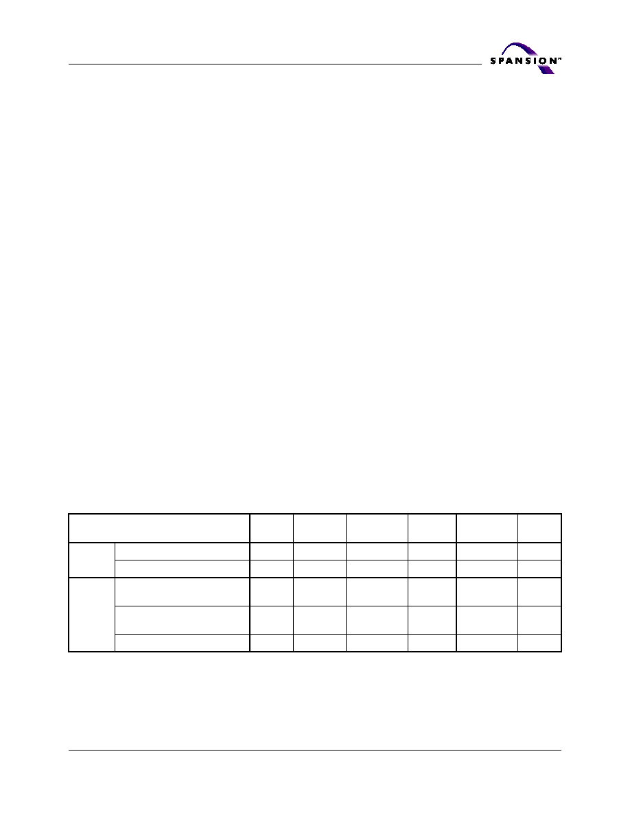
November 5, 2004 S29CD016_00_A4
S29CD016G
65
A d v a n c e I n f o r m a t i o n
DQ5: Exceeded Timing Limits
DQ5 indicates whether the program or erase time exceeded a specified internal
pulse count limit. Under these conditions DQ5 produces a "1." This is a failure
condition that indicates the program or erase cycle was not successfully
completed.
The DQ5 failure condition may appear if the system tries to program a "1" to a
location that is previously programmed to "0." Only an erase operation can
change a "0" back to a "1." Under this condition, the device halts the opera-
tion, and when the operation exceeds the timing limits, DQ5 produces a "1."
Under both these conditions, the system must issue the reset command to return
the device to reading array data.
DQ3: Sector Erase Timer
After writing a sector erase command sequence, the system may read DQ3 to de-
termine whether or not an erase operation started. (The sector erase timer does
not apply to the chip erase command.) If additional sectors are selected for era-
sure, the entire time-out also applies after each additional sector erase
command. When the time-out is complete, DQ3 switches from "0" to "1." The
system may ignore DQ3 if the system can guarantee that the time between ad-
ditional sector erase commands is always less than 50 µs. See also
"Sector
Erase Command" on page 48
.
After the sector erase command sequence is written, the system should read the
status on DQ7 (Data# Polling) or DQ6 (Toggle Bit I) to ensure the device accepted
the command sequence, and then read DQ3. If DQ3 is "1", the internally con-
trolled erase cycle started; all further commands (other than Erase Suspend) are
ignored until the erase operation is complete. If DQ3 is "0", the device accepts
additional sector erase commands. To ensure the command was accepted, the
system software should check the status of DQ3 prior to and following each sub-
sequent sector erase command. If DQ3 is high on the second status check, the
last command might not have been accepted.
Table 21 on page 65
shows the
outputs for DQ3.
Table 21. Write Operation Status
Notes:
1. DQ5 switches to `1' when an Embedded Program or Embedded Erase operation exceeds the maximum timing limits.
See
"DQ5: Exceeded Timing Limits" on page 65
for more information.
2. DQ7 and DQ2 require a valid address when reading status information. Refer to the appropriate subsection for further
details.
Operation
DQ7
(Note 2)
DQ6
DQ5
(Note 1)
DQ3
DQ2
(Note 2)
RY/BY#
Standard
Mode
Embedded Program Algorithm
DQ7#
Toggle
0
N/A
No toggle
0
Embedded Erase Algorithm
0
Toggle
0
1
Toggle
0
Erase
Suspend
Mode
Reading within Erase
Suspended Sector
1
No toggle
0
N/A
Toggle
1
Reading within Non-Erase
Suspended Sector
Data
Data
Data
Data
Data
1
Erase-Suspend-Program
DQ7#
Toggle
0
N/A
N/A
0
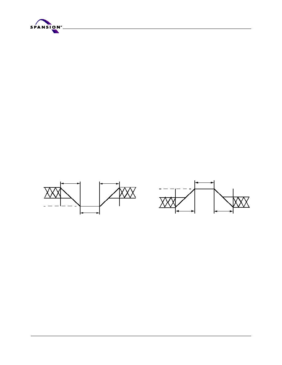
66
S29CD016G
S29CD016_00_A4 November 5, 2004
A d v a n c e I n f o r m a t i o n
Absolute Maximum Ratings
Storage Temperature, Plastic Packages. . . . . . . . . . . . . . . . ≠65∞C to +150∞C
Ambient Temperature with Power Applied . . . . . . . . . . . . . . ≠65∞C to +145∞C
V
CC
, V
IO
(Note 1) . . . . . . . . . . . . . . . . . . . . . . . . . . . . . . . ≠0.5 V to + 3.0 V
ACC, A9, OE#, and RESET# (Note 2) . . . . . . . . . . . . . . . . . ≠0.5 V to +13.0 V
Address, Data, Control Signals
(Note 1) . . . . . . . . . . . . . . . . . . . . . . . . . . . . . . . . . ≠0.5 V to 3.60 V
All other pins (Note 1) . . . . . . . . . . . . . . . . . . . . . . . ≠0.5 V to +3.60 V
Output Short Circuit Current (Note 3). . . . . . . . . . . . . . . . . . . . . . . . 200 mA
Notes:
1. Minimum DC voltage on input or I/O pins is ≠0.5 V. During voltage transitions, input at I/O pins may overshoot V
SS
to ≠2.0 V for periods of up to 20 ns. See 6. Maximum DC voltage on output and I/O pins is 3.6 V. During voltage
transitions output pins may overshoot to V
CC
+ 2.0 V for periods up to 20 ns. See Figure 6.
2. Minimum DC input voltage on pins ACC, A9, OE#, and RESET# is -0.5 V. During voltage transitions, A9, OE#, and
RESET# may overshoot V
SS
to ≠2.0 V for periods of up to 20 ns. See Figure 5. Maximum DC input voltage on pin
A9 and OE# is +13.0 V which may overshoot to 14.0 V for periods up to 20 ns.
3. No more than one output may be shorted to ground at a time. Duration of the short circuit should not be greater
than one second.
4. Stresses above those listed under "Absolute Maximum Ratings" may cause permanent damage to the device. This is
a stress rating only; functional operation of the device at these or any other conditions above those indicated in the
operational sections of this data sheet is not implied. Exposure of the device to absolute maximum rating conditions
for extended periods may affect device reliability.
Operating Ranges
Industrial (I) Devices
Ambient Temperature (T
A
) . . . . . . . . . . . . . . . . . . . . . . . . . ≠40∞C to +85∞C
Extended (E) Devices
Ambient Temperature (T
A
) . . . . . . . . . . . . . . . . . . . . . . . . ≠40∞C to +125∞C
V
CC
Supply Voltages
V
CC
for regulated voltage range . . . . . . . . . . . . . . . . . . . . . . . 2.5 V to 2.75 V
V
IO
Supply Voltages
V
IO
. . . . . . . . . . . . . . . . . . . . . . . . . . . . . . . . . . . . . . . 1.65 V to 2.75 V
Operating ranges define those limits between which the functionality of the device is guaranteed.
Figure 8. Maximum Negative Overshoot
Waveform
Figure 9. Maximum Positive Overshoot Waveform
20 ns
20 ns
+0.8 V
≠0.5 V
20 ns
≠2.0 V
20 ns
20 ns
V
CC
+2.0 V
V
CC
+0.5 V
20 ns
2.0 V
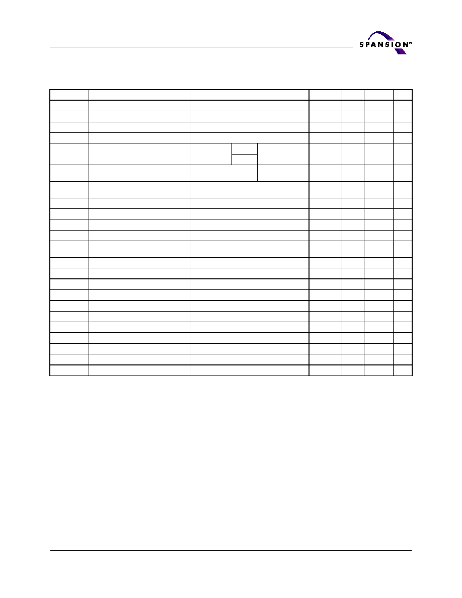
November 5, 2004 S29CD016_00_A4
S29CD016G
67
A d v a n c e I n f o r m a t i o n
DC Characteristics
Notes:
1. The I
CC
current listed includes both the DC operating current and the frequency dependent component.
2. I
CC
active while Embedded Erase or Embedded Program is in progress.
3. Not 100% tested.
4. Maximum I
CC
specifications are tested with V
CC
= V
CCmax
.
5. Current maximum was increased significantly from data sheet Revision B+4, Dated April 8, 2003.
6. Pull-up 6resistor is required.
Table 22. CMOS Compatible
Parameter
Description
Test Conditions
Min
Typ
Max
Unit
I
LI
Input Load Current
V
IN
= V
SS
to V
IO
, V
IO
= V
IO
max
±1.0
µA
I
LIWP
WP# Input Load Current
V
IN
= V
SS
to V
IO
, V
IO
= V
IO
max
≠25
µA
I
LIT
A9, ACC Input Load Current
V
CC
= V
CCmax
; A9 = 12.5 V
35
µA
I
LO
Output Leakage Current
V
OUT
= V
SS
to V
CC
, V
CC
= V
CC max
±1.0
µA
I
CCB
V
CC
Active Burst Read Current
(Note 1)
CE# = V
IL
,
OE# =
V
IL
56 MHz
8 Double-Word
70
90
mA
66 MHz
I
CC1
V
CC
Active Asynchronous Read Current
(Note 1)
CE# = V
IL
,
OE# =
V
IL
1 MHz
10
mA
I
CC3
V
CC
Active Program Current
(Notes 2, 4)
CE# = V
IL
,
OE# = V
IH
, ACC = V
IH
40
50
mA
I
CC4
V
CC
Active Erase Current (Notes 2, 4)
CE# = V
IL
,
OE# = V
IH
, ACC = V
IH
20
50
mA
I
CC5
V
CC
Standby Current (CMOS) (Note 5) V
CC
= V
CC max
, CE# = V
CC
± 0.3 V
60
µA
I
CC6
V
CC
Active Current (Read While Write) CE# = V
IL
,
OE# = V
IL
30
90
mA
I
CC7
V
CC
Reset Current (Note 5)
RESET# = V
IL
60
µA
I
CC8
Automatic Sleep Mode Current (Note
5)
V
IH
= V
CC
± 0.3 V, V
IL
= V
SS
± 0.3 V
60
µA
I
ACC
V
ACC
Acceleration Current
ACC = V
HH
20
mA
V
IL
Input Low Voltage
≠0.5
0.3 x V
IO
V
V
IH
Input High Voltage
0.7 x V
IO
3.6
V
V
ILCLK
CLK Input Low Voltage
≠0.2
0.3 x V
IO
V
V
IHCLK
CLK Input High Voltage
0.7 x V
CC
2.75
V
V
ID
Voltage for Autoselect
V
CC
= 2.5 V
11.5
12.5
V
V
OL
Output Low Voltage
I
OL
= 4.0 mA, V
CC
= V
CC min
0.4
V
I
OLRB
RY/BY#, Output Low Current (Note 6) V
OL
= 0.4 V
1
mA
V
HH
Accelerated (ACC pin) High Voltage
V
CC
= V
CC min
11.5
12.5
V
V
OH
Output High Voltage
I
OH
= ≠100 µA, V
CC
= V
CC min
V
IO
≠0.4
V
V
LKO
Low V
CC
Lock-Out Voltage (Note 3)
1.6
2.0
V
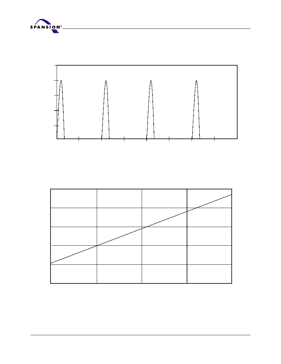
68
S29CD016G
S29CD016_00_A4 November 5, 2004
A d v a n c e I n f o r m a t i o n
DC Characteristics (continued)
Zero Power Flash
Note: Addresses are switching at 1 MHz
Figure 10. I
CC1
Current vs. Time (Showing Active and Automatic Sleep Currents)
5
4
3
2
1
0
0
500
1000
1500
2000
2500
3000
3500
4000
S
u
p
p
ly
C
u
r
r
en
t
in
mA
Time in ns
20
16
4
0
1
2
3
4
5
Frequency in MHz
S
u
p
p
ly
C
u
r
r
en
t
in
mA
Note: T = -40 ∞C
Figure 11. Typical I
CC1
vs. Frequency
2.7 V
8
12

November 5, 2004 S29CD016_00_A4
S29CD016G
69
A d v a n c e I n f o r m a t i o n
Test Conditions
Key to Switching Waveforms
Switching Waveforms
Table 23. Test Specifications
Test Condition
40 Mhz (OJ),
56 Mhz (OM)
66 Mhz (OP)
Unit
Output Load
1 TTL gate
Output Load Capacitance, C
L
(including jig capacitance)
30
100
pF
Input Rise and Fall Times
5
ns
Input Pulse Levels
0.0 V ≠ V
IO
V
Input timing measurement reference levels
V
IO
/2
V
Output timing measurement reference levels
V
IO
/2
V
Figure 12. Test Setup
Note: Diodes are IN3064 or equivalent
CL
Device
Under
Test
Waveform
Inputs
Outputs
Steady
Changing from H to L
Changing from L to H
Don't Care, Any Change Permitted
Changing, State Unknown
Does Not Apply
Center Line is High Impedance State (High Z)
V
IO
V
SS
V
IO
/2 V
IO
/2
Output
Measurement Level
In
Figure 13. Input Waveforms and Measurement Levels
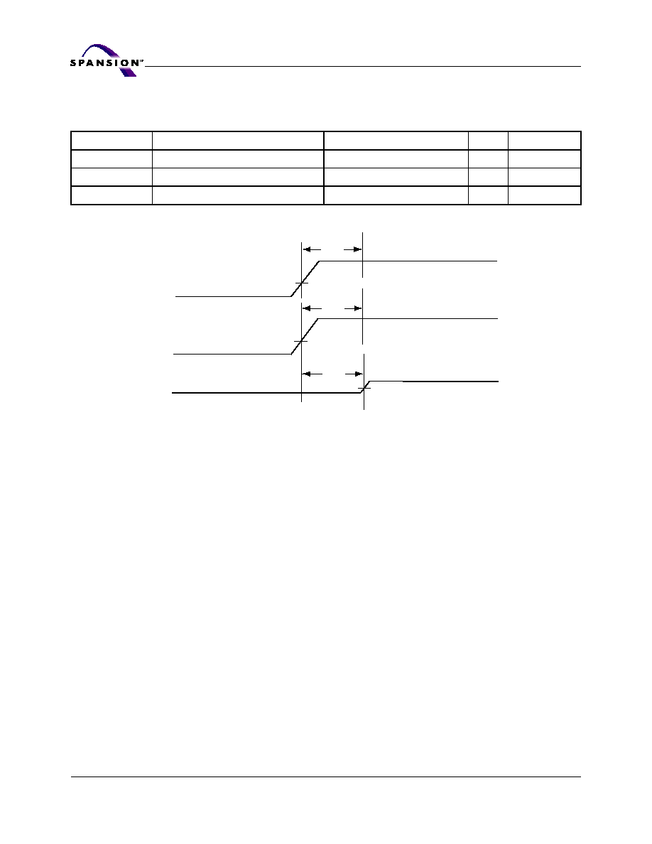
70
S29CD016G
S29CD016_00_A4 November 5, 2004
A d v a n c e I n f o r m a t i o n
AC Characteristics
V
CC
and V
IO
Power-up
Figure 14. V
CC
and V
IO
Power-up Diagram
Parameter
Description
Test Setup
Speed
Unit
t
VCS
V
CC
Setup Time
Min
50
µs
t
VIOS
V
IO
Setup Time
Min
50
µs
t
RSTH
RESET# Low Hold Time
Min
50
µs
V
CC
V
IOP
RESET#
t
VCS
t
RSTH
t
VIOS
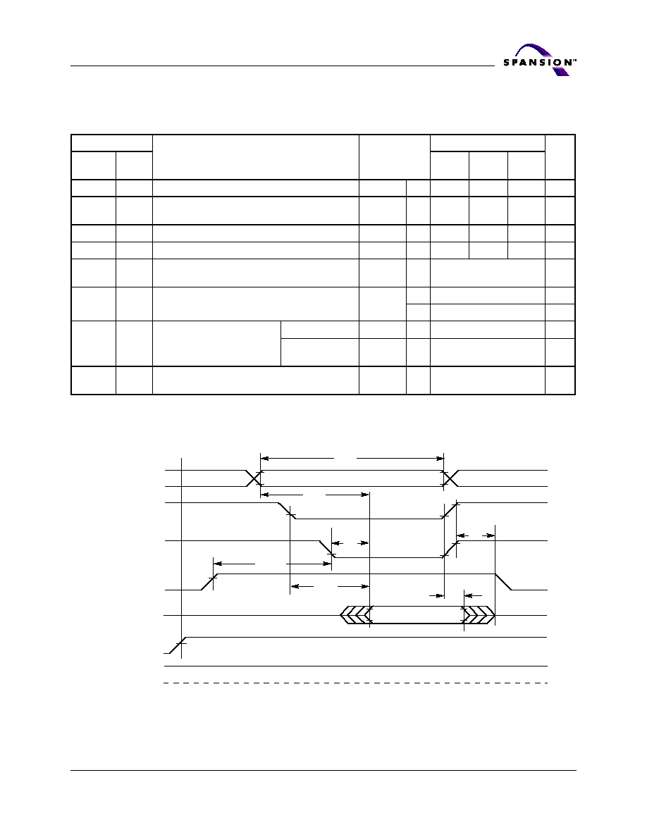
November 5, 2004 S29CD016_00_A4
S29CD016G
71
A d v a n c e I n f o r m a t i o n
AC Characteristics
Table 24. Asynchronous Read Operations
Notes:
1. Not 100% tested.
2. See
Figure 12, on page 69
and
Table 23 on page 69
for test specifications
Figure 15. Conventional Read Operations Timings
Parameter
Description
Test Setup
Speed Options
Unit
JEDEC
Std.
66 Mhz
(OP)
55 Mhz
(OM)
40 Mhz
(OJ)
t
AVAV
t
RC
Read Cycle Time (Note 1)
Max
54
64
67
ns
t
AVQV
t
ACC
Address to Output Delay
CE# = V
IL
OE# = V
IL
Max
54
64
67
ns
t
ELQV
t
CE
Chip Enable to Output Delay
OE# = V
IL
Max
58
69
71
ns
t
GLQV
t
OE
Output Enable to Output Delay
Max
20
20
28
ns
t
EHQZ
t
DF
Chip Enable to Output High Z
(Note 1)
Max
10
ns
t
GHQZ
t
DF
Output Enable to Output High Z (Note 1)
Min
2
ns
Max
10
ns
t
OEH
Output Enable
Hold Time (Note 1)
Read
Min
0
ns
Toggle and
Data# Polling
Min
10
ns
t
AXQX
t
OH
Output Hold Time From Addresses, CE# or OE#,
Whichever Occurs First (Note 1)
Min
2
ns
t
CE
Outputs
WE#
Addresses
CE#
OE#
HIGH Z
Output Valid
HIGH Z
Addresses Stable
t
RC
t
ACC
t
OEH
t
OE
0 V
RY/BY#
RESET#
t
DF
t
OH

72
S29CD016G
S29CD016_00_A4 November 5, 2004
A d v a n c e I n f o r m a t i o n
AC Characteristics
Table 25. Burst Mode Read
Parameter
Description
Speed Options
Unit
JEDEC
Std.
66 Mhz (0P)
56 Mhz
(0M)
40 Mhz
(0J)
t
BACC
Burst Access Time Valid Clock to Output Delay
Max
9 FBGA
9.5 PQFP
10 FBGA
10 PQFP
17
ns
t
ADVCS
ADV# Setup Time to Rising Edge of CLK
Min
6
ns
t
ADVCH
ADV# Hold Time from Rising Edge of CLK
Min
1.5
1.5
1.5
ns
t
ADVP
ADV# Pulse Width
Min
13
15
22
ns
t
DVCH
Valid Data Hold from CLK
Min
2
3
3
ns
t
DIND
CLK to Valid IND/WAIT#
Max
9 FBGA
9.5 PQFP
10 FBGA
10 PQFP
17
ns
t
INDH
IND/WAIT# Hold from CLK
Min
2
3
3
ns
t
IACC
CLK to Valid Data Out, Initial Burst Access
Max
54.45
63.55
67
ns
t
CLK
CLK Period
Min
15.15
17.85
25
ns
Max
60
3
3
t
CR
CLK Rise Time
Max
ns
t
CF
CLK Fall Time
Max
ns
t
CH
CLK High Time
Min
2.5
2.5
3
ns
t
CL
CLK Low Time
Min
2.5
2.5
3
ns
t
DS
Data Setup to WE# Rising Edge
Min
18
ns
t
DH
Data Hold from WE# Rising Edge
Min
2
ns
t
AS
Address Setup to Falling Edge of WE#
Min
0
ns
t
AH
Address Hold from Falling Edge of WE#
Min
22
23
24
ns
t
CS
CE# Setup Time
Min
4
ns
t
CH
CE# Hold Time
Min
3
ns
t
ACS
Address Setup Time to CLK
Min
6
ns
t
ACH
Address Hold Time from ADV# Rising Edge of CLK
while ADV# is Low
Min
5
ns
t
OE
Output Enable to Output Valid
Max
20
20
28
ns
t
DF
t
OEZ
Output Enable to Output High Z
Min
2
3
3
ns
Max
10
15
17
t
EHQZ
t
CEZ
Chip Enable to Output High Z
Max
10
15
17
ns
t
CES
CE# Setup Time to Clock
Min
6
ns
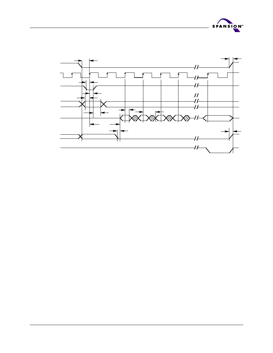
November 5, 2004 S29CD016_00_A4
S29CD016G
73
A d v a n c e I n f o r m a t i o n
AC Characteristics
Figure 16. Burst Mode Read (x32 Mode)
Da
Da + 2
Da + 3
Da + 31
OE#*
Data
Addresses
Aa
IND#
ADV#
CLK
CE#
t
CES
t
ACS
t
ADVCS
t
ADVCH
t
ACH
t
OE
t
BACC
t
BDH
t
OEZ
t
CEZ
t
IACC
Da + 1
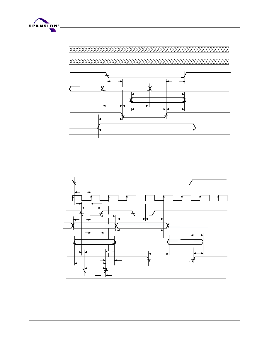
74
S29CD016G
S29CD016_00_A4 November 5, 2004
A d v a n c e I n f o r m a t i o n
AC Characteristics
Figure 17. Asynchronous Command Write Timing
Note: All commands have the same number of cycles in both asynchronous and synchronous modes, including the
READ/RESET command. Only a single array access occurs after the F0h command is entered. All subsequent accesses
are burst mode when the burst mode option is enabled in the Configuration Register.
Figure 18. Synchronous Command Write/Read Timing
Note: All commands have the same number of cycles in both asynchronous and synchronous modes, including the
READ/RESET command. Only a single array access occurs after the F0h command is entered. All subsequent accesses
are burst mode when the burst mode option is enabled in the Configuration Register.
ADV#
CE#
Valid Data
Addresses
Data
WE#
OE#
IND/WAIT#
CLK
Stable Address
t
CS
t
CH
t
AS
t
AH
t
OEH
t
DS
t
DH
t
WPH
t
WC
t
AS
CLK
ADV#
Data In
Addresses
Data
OE#
Data Out
WE#
IND/WAIT#
CE#
Valid Address
t
DS
t
WP
t
CES
t
ADVP
t
ADVCS
t
OE
t
ACS
t
ACS
t
DF
t
EHQZ
t
DH
t
WADVH
t
ADVCH
tWADVH2
t
ACH
t
WC
t
AP
t
WCKS
Valid
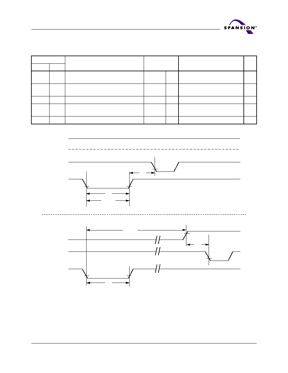
November 5, 2004 S29CD016_00_A4
S29CD016G
75
A d v a n c e I n f o r m a t i o n
AC Characteristics
Note: Not 100% tested.
Table 26. Hardware Reset (RESET#)
Parameter
Description
All Speed Options
JEDEC
Std.
Test Setup
Unit
t
READY
RESET# Pin Low (During Embedded
Algorithms) to Read or Write (See Note)
Max
11
µs
t
READY
RESET# Pin Low (NOT During Embedded
Algorithms) to Read or Write (See Note)
Max
500
ns
t
RP
RESET# Pulse Width
Min
500
ns
t
RH
RESET# High Time Before Read (See
Note)
Min
50
ns
t
RPD
RESET# Low to Standby Mode
Min
20
µs
RESET#
RY/BY#
RY/BY#
t
RP
t
Ready
Reset Timing to Bank NOT Executing Embedded Algorithm
t
Ready
CE#, OE#
t
RH
CE#, OE#
Reset Timing to Bank Executing Embedded Algorithm
RESET#
t
RP
t
RB
Figure 19. RESET# Timings
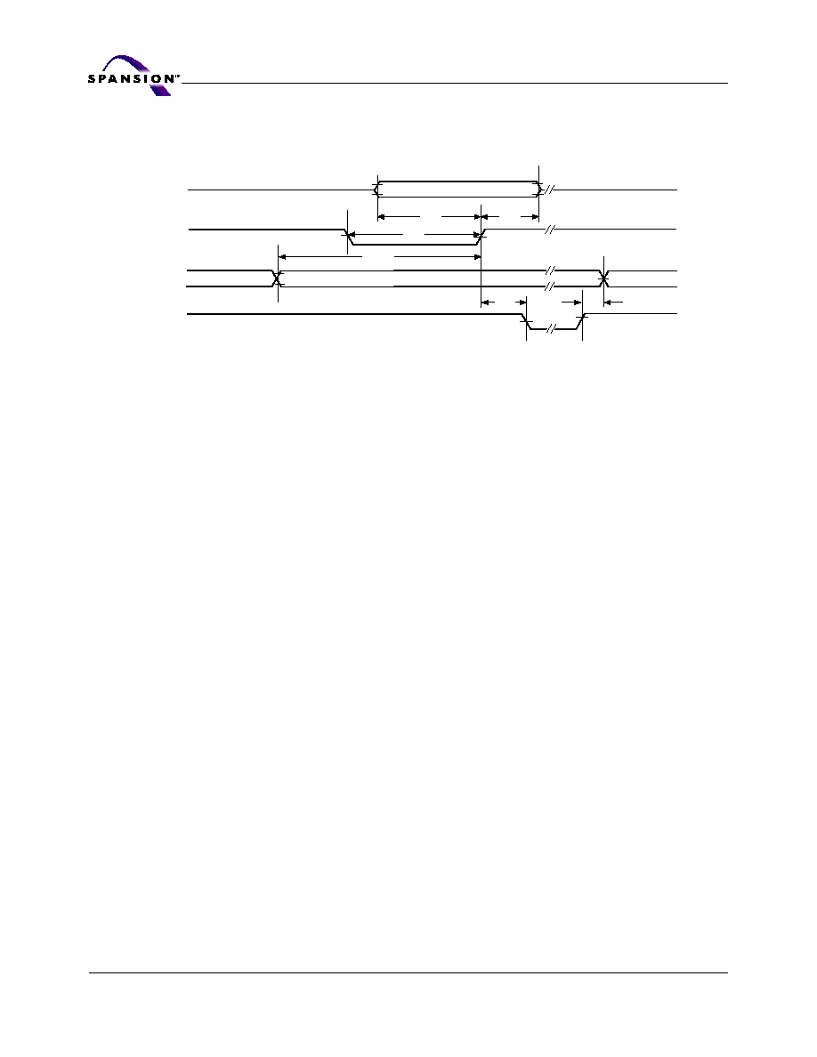
76
S29CD016G
S29CD016_00_A4 November 5, 2004
A d v a n c e I n f o r m a t i o n
AC Characteristics
Figure 20. WP# Timing
Program/Erase Command
WP#
Data
Valid WP#
t
CH
t
DS
t
DH
WE#
RY/BY#
t
WPWS
t
WPRH
t
WP
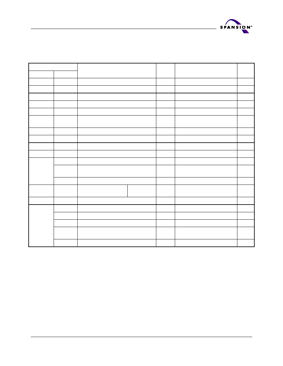
November 5, 2004 S29CD016_00_A4
S29CD016G
77
A d v a n c e I n f o r m a t i o n
AC Characteristics
Erase/Program Operations
Notes:
1. Not 100% tested.
2. See
Table 29 on page 85
for more information.
Table 27. Erase/Program Operations
Parameter
All Speed Options
JEDEC
Std.
Description
Unit
t
AVAV
t
WC
Write Cycle Time (Note 1)
Min
60
ns
t
AVWL
t
AS
Address Setup Time
Min
0
ns
t
WLAX
t
AH
Address Hold Time
Min
25
ns
t
DVWH
t
DS
Data Setup to WE# Rising Edge
Min
15
ns
t
WHDX
t
DH
Data Hold from WE# Rising Edge
Min
2
ns
t
GHWL
t
GHWL
Read Recovery Time Before Write
(OE# High to WE# Low)
Min
0
ns
t
ELWL
t
CS
CE# Setup Time
Min
0
ns
t
WHEH
t
CH
CE# Hold Time
Min
2
ns
t
WLWH
t
WP
WE# Width
Min
25
ns
t
WHWL
t
WPH
Write Pulse Width High
Min
30
ns
t
WADVH1
WE# Falling Edge After ADV# Falling Edge
Min
0
ns
t
WADVH2
WE# Rising Edge After ADV# Rising
Edge
Min
10
ns
t
WCKS
WE# Rising Edge Setup to CLK Rising Edge
Min
5
ns
t
WHWH1
t
WHWH1
Programming Operation
(Note 2)
Double-Word
Typ
18
µs
t
WHWH2
t
WHWH2
Sector Erase Operation (Note 2)
Typ
1.0
sec.
t
VCS
V
CC
Setup Time (Note 1)
Min
50
µs
t
RB
Recovery Time from RY/BY#
Min
0
ns
t
BUSY
RY/BY# Delay After WE# Rising Edge
Max
90
ns
t
WPWS
WP# Setup to WE# Rising Edge with
Command
Min
20
ns
t
WPRH
WP# Hold after RY/BY# Rising Edge
Max
2
ns
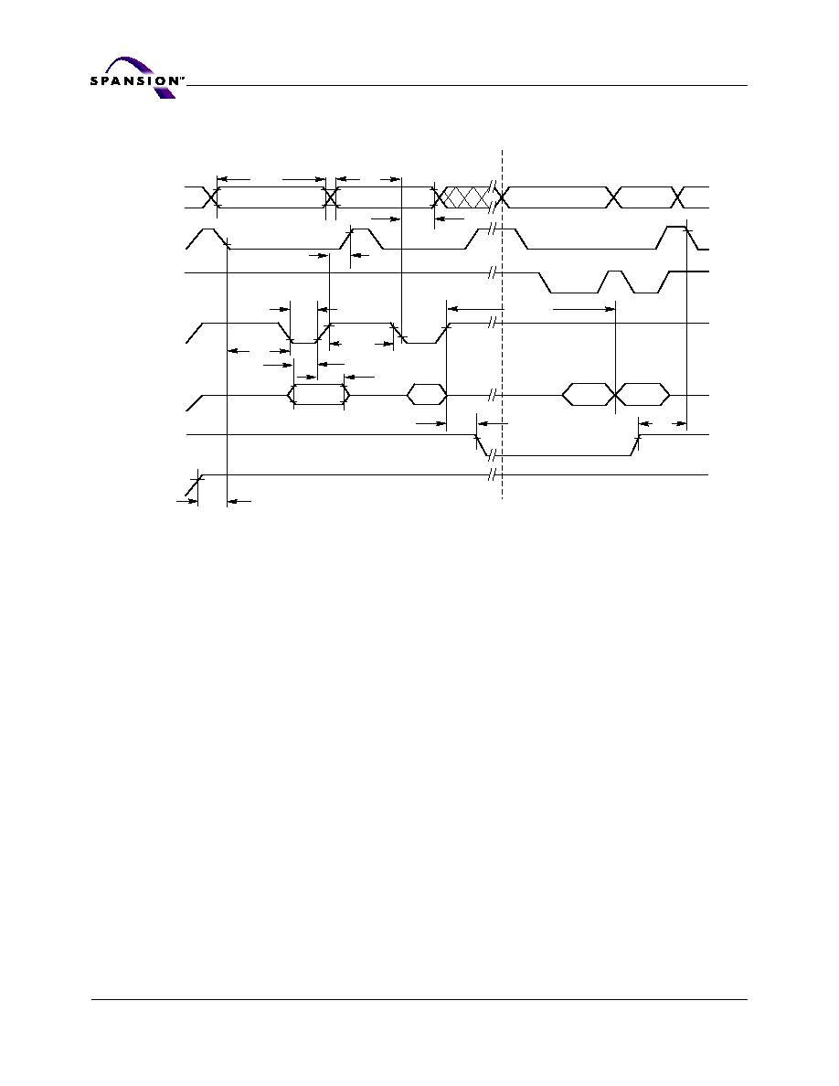
78
S29CD016G
S29CD016_00_A4 November 5, 2004
A d v a n c e I n f o r m a t i o n
AC Characteristics
Notes: PA = program address, PD = program data, D
OUT
is the true data at the program address.
Figure 21. Program Operation Timings
OE#
WE#
CE#
V
CC
Data
Addresses
t
DS
t
AH
t
DH
t
WP
PD
t
WHWH1
t
WC
t
AS
t
WPH
t
VCS
555h
PA
PA
Read Status Data (last two cycles)
A0h
t
CS
Statu
D
OUT
Program Command Sequence (last two cycles)
RY/BY#
t
RB
t
BUSY
t
CH
PA
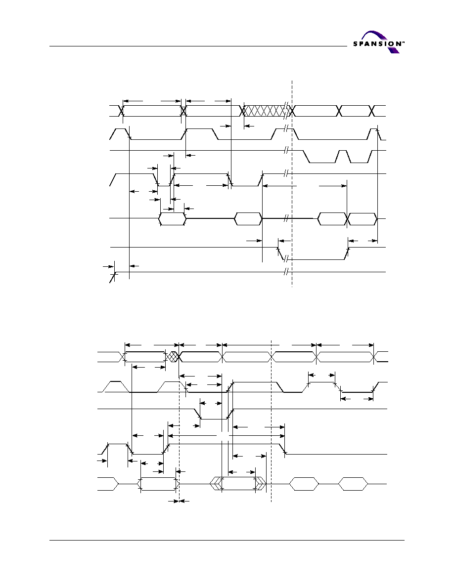
November 5, 2004 S29CD016_00_A4
S29CD016G
79
A d v a n c e I n f o r m a t i o n
AC Characteristics
Note: SA = sector address (for Sector Erase), VA = Valid Address for reading status data (see
Table 21 on page 65
).
Figure 22. Chip/Sector Erase Operation Timings
Figure 23. Back-to-back Cycle Timings
OE#
CE#
Addresses
V
CC
WE#
Data
2AAh
SA
t
AH
t
WP
t
WC
t
AS
t
WPH
555h for chip erase
10 for Chip Erase
t
DS
t
VCS
t
CS
t
DH
t
CH
t
WHWH2
VA
VA
Erase Command Sequence (last two cycles)
Read Status Data
RY/BY#
t
RB
t
BUSY
55h
30h
In
Progress
Complete
OE#
CE#
WE#
Addresses
t
OH
Data
Valid
In
Valid
In
Valid PA
Valid RA
t
WC
t
WPH
t
AH
t
WP
t
DS
t
DH
t
RC
t
CE
Valid
Out
t
OE
t
ACC
t
OEH
t
GHWL
t
DF
Valid
In
CE# Controlled Write Cycles
WE# Controlled Write Cycle
Valid PA
Valid PA
t
CP
t
CPH
t
WC
t
WC
Read Cycle
t
SR/W
t
WPH
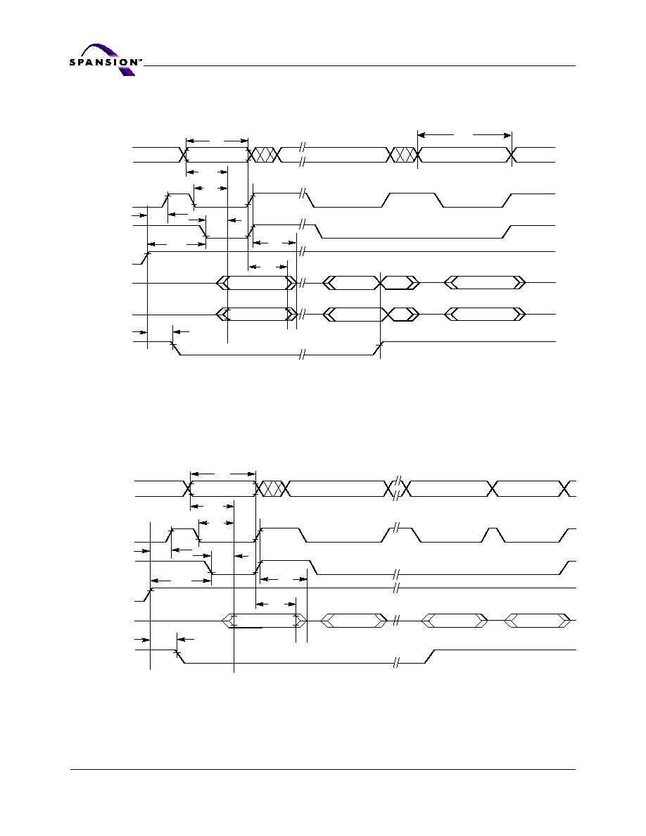
80
S29CD016G
S29CD016_00_A4 November 5, 2004
A d v a n c e I n f o r m a t i o n
AC Characteristics
WE#
CE#
OE#
High Z
t
OE
High Z
DQ7
Data
RY/BY#
t
BUSY
Complement
True
Addresses
VA
t
OEH
t
CE
t
CH
t
OH
t
DF
VA
VA
Status Data
Complement
Status Data
True
Valid Data
Valid Data
t
ACC
t
RC
t
WC
Note: VA = Valid address. Illustration shows first status cycle after command sequence, last status read cycle, and array
data read cycle.
Figure 24. Data# Polling Timings
(During Embedded Algorithms)
WE#
CE#
OE#
High Z
t
OE
DQ6/DQ2
RY/BY#
t
BUSY
Addresses
VA
t
OEH
t
CE
t
CH
t
OH
t
DF
VA
VA
t
ACC
t
RC
Valid Data
Valid Status
Valid Status
(first read)
(second read)
(stops toggling)
Valid Status
VA
Note: VA = Valid address; not required for DQ6. Illustration shows first two status cycle after command sequence, last
status read cycle, and array data read cycle.
Figure 25. Toggle Bit Timings
(During Embedded Algorithms)
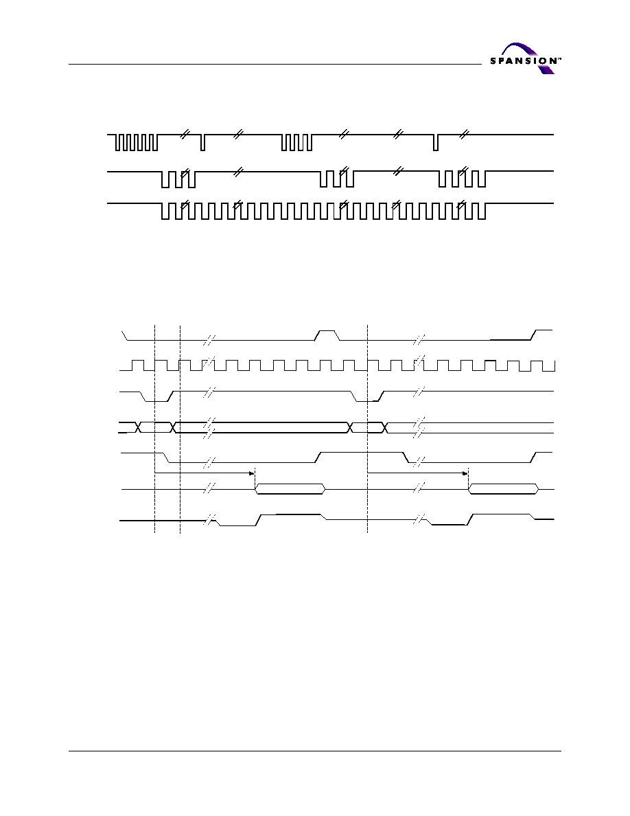
November 5, 2004 S29CD016_00_A4
S29CD016G
81
A d v a n c e I n f o r m a t i o n
AC Characteristics
Note: The system may use CE# or OE# to toggle DQ2 and DQ6. DQ2 toggles only when read at an address within an
erase-suspended sector.
Figure 26. DQ2 vs. DQ6 for Erase/Erase Suspend Operations
Enter
Erase
Erase
Erase
Enter Erase
Suspend Program
Erase Suspend
Read
Erase Suspend
Read
Erase
WE#
DQ6
DQ2
Erase
Complete
Erase
Suspend
Suspend
Program
Resume
Embedded
Erasing
CE#
CLK
AVD#
Addresses
OE#
Data
RDY
Status Data
Status Data
V A
V A
t
OE
t
OE
Notes:
1. The timings are similar to synchronous read timings and asynchronous data polling Timings/Toggle bit Timing.
2. VA = Valid Address. Two read cycles are required to determine status. When the Embedded Algorithm operation
is complete, the toggle bits stops toggling.
3. RDY is active with data (A18 = 0 in the Configuration Register). When A18 = 1 in the Configuration Register, RDY
is active one clock cycle before data.
4. Data polling requires burst access time delay.
Figure 27. Synchronous Data Polling Timing/Toggle Bit Timings

82
S29CD016G
S29CD016_00_A4 November 5, 2004
A d v a n c e I n f o r m a t i o n
AC Characteristics
Sector Protect: 150 µs
Sector Unprotect: 15 ms
1 µs
RESET#
SA, A6,
A1, A0
Data
CE#
WE#
OE#
60h
60h/68h**
40h/48h***
Valid*
Valid*
Valid*
Status
Sector Protect/Unprotect
Verify
V
IH
* Valid address for sector protect: A[7:0] = 3Ah. Valid address for sector unprotect: A[7:0] = 3Ah.
** Command for sector protect is 68h. Command for sector unprotect is 60h.
*** Command for sector protect verify is 48h. Command for sector unprotect verify is 40h.
Figure 28. Sector Protect/Unprotect Timing Diagram

November 5, 2004 S29CD016_00_A4
S29CD016G
83
A d v a n c e I n f o r m a t i o n
AC Characteristics
Table 28. Alternate CE# Controlled Erase/Program Operations
Notes:
1. Not 100% tested.
2. See the section for more information.
Parameter
All Speed Options
JEDEC
Std.
Description
Unit
t
AVAV
t
WC
Write Cycle Time (Note 1)
Min
65
ns
t
AVEL
t
AS
Address Setup Time
Min
0
ns
t
ELAX
t
AH
Address Hold Time
Min
45
ns
t
DVEH
t
DS
Data Setup Time
Min
35
ns
t
EHDX
t
DH
Data Hold Time
Min
2
ns
t
OES
Output Enable Setup Time
Min
0
ns
t
GHEL
t
GHEL
Read Recovery Time Before Write
(OE# High to WE# Low)
Min
0
ns
t
WLEL
t
WS
WE# Setup Time
Min
0
ns
t
EHWH
t
WH
WE# Hold Time
Min
0
ns
t
WP
WE# Width
Min
32
ns
t
WPH
Write Pulse Width High
Min
40
ns
t
WADVH
WE# Falling Edge After
Min
0
ns
t
WCKS
WE# Rising Edge Setup to Clk Rising Edge
Min
5
ns
t
ELEH
t
CP
CE# Pulse Width
Min
16
ns
t
EHEL
t
CPH
CE# Pulse Width High
Min
30
ns
t
WHWsH1
t
WHWH1
Programming Operation
(Note 2)
Double-Word
Typ
18
µs
t
WHWH2
t
WHWH2
Sector Erase Operation (Note 2)
Typ
1.0
sec.
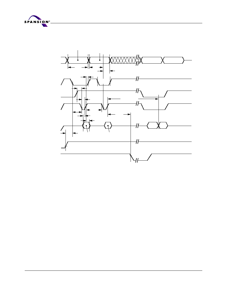
84
S29CD016G
S29CD016_00_A4 November 5, 2004
A d v a n c e I n f o r m a t i o n
AC Characteristics
t
GHEL
t
WS
OE#
CE#
WE#
RESET#
t
DS
Data
t
AH
Addresses
t
DH
t
CP
DQ7#
D
OUT
t
WC
t
AS
t
CPH
PA
Data# Polling
A0 for program
55 for erase
t
RH
t
WHWH1 or 2
RY/BY#
t
WH
PD for program
30 for sector erase
10 for chip erase
555 for program
2AA for erase
PA for program
SA for sector erase
555 for chip erase
t
BUSY
t
WPH
t
WP
Notes:
1. PA = program address, PD = program data, DQ7# = complement of the data written to the device, D
OUT
= data
written to the device.
2. The figure indicates the last two bus cycles of the command sequence.
Figure 29. Alternate CE# Controlled Write Operation Timings

November 5, 2004 S29CD016_00_A4
S29CD016G
85
A d v a n c e I n f o r m a t i o n
Table 29. Erase and Programming Performance
Notes:
1. Typical program and erase times assume the following conditions: 25
∞
C, 2.5 V V
CC
, 100,000 cycles. Additionally,
programming typicals assume checkerboard pattern.
2. Under worst case conditions of 145∞C, V
CC
= 2.5 V, 1,000,000 cycles.
3. The typical chip programming time is considerably less than the maximum chip programming time listed.
4. In the pre-programming step of the Embedded Erase algorithm, all bytes are programmed to 00h before erasure.
5. System-level overhead is the time required to execute the two- or four-bus-cycle sequence for the program
command. See
Table 19 on page 58
and
Table 20 on page 59
for further information on command definitions.
6. PPBs have a program/erase cycle endurance of 100 cycles.
Table 30. PQFP and Fortified BGA Pin Capacitance
Notes:
1. Sampled, not 100% tested.
2. Test conditions T
A
= 25∞C, f = 1.0 MHz.
Parameter
Typ (Note 1)
Max (Note 2)
Unit
Comments
Sector Erase Time
1.0
5
s
Excludes 00h programming
prior to erasure (Note 4)
Chip Erase Time
46
230
s
Double Word Program Time
18
250
µs
Excludes system level
overhead (Note 5)
Accelerated Double Word Program Time
8
130
µs
Accelerated Chip Program Time
5
50
s
Chip Program Time
(Note 3)
x32
12
120
s
Parameter
Symbol
Parameter Description
Test Setup
Typ
Max
Unit
C
IN
Input Capacitance
V
IN
= 0
6
7.5
pF
C
OUT
Output Capacitance
V
OUT
= 0
8.5
12
pF
C
IN2
Control Pin Capacitance
V
IN
= 0
7.5
9
pF

86
S29CD016G
S29CD016_00_A4 November 5, 2004
A d v a n c e I n f o r m a t i o n
Physical Dimensions
PRQ080≠80-Lead Plastic Quad Flat Package
3213\38.4C
PACKAGE
PQR 080
JEDEC
MO-108(B)CB-1
NOTES
SYMBOL
MIN
NOM
MAX
A
--
--
3.35
A1
0.25
--
--
A2
2.70
2.80
2.90
b
0.30
--
0.45
SEE NOTE 4
c
0.15
--
0.23
D
17.00
17.20
17.40
D1
13.90
14.00
14.10
SEE NOTE 3
D3
--
12.0
--
REFERENCE
e
--
0.80
--
BASIC, SEE NOTE 7
E
23.00
23.20
23.40
E1
19.90
20.00
20.10
SEE NOTE 3
E3
--
18.40
--
REFERENCE
aaa
---
0.20
---
ccc
0.10
L
0.73
0.88
1.03
P
24
Q
40
R
64
S
80
NOTES:
1.
ALL DIMENSIONS AND TOLERANCES CONFORM TO
ANSI Y14.5M-1982.
2.
DATUM PLANE -A- IS LOCATED AT THE MOLD PARTING LINE
AND IS COINCIDENT WITH THE BOTTOM OF THE LEAD WHERE
THE LEAD EXITS THE PLASTIC BODY.
3.
DIMENSIONS "D1" AND "E1" DO NOT INCLUD MOLD PROTRUSION.
ALLOWABLE PROTRUSION IS 0.25 mm PER SIDE.
DIMENSIONS "D1" AND "E1" INCLUDE MOLD MISMATCH AND
ARE DETERMINED AT DATUM PLANE -A-
4.
DIMENSION "B" DOES NOT INCLUDE DAMBAR PROTRUSION.
5.
CONTROLLING DIMENSIONS: MILLIMETER.
6.
DIMENSIONS "D" AND "E" ARE MEASURED FROM BOTH
INNERMOST AND OUTERMOST POINTS.
7.
DEVIATION FROM LEAD-TIP TRUE POSITION SHALL BE WITHIN
±0.0076 mm FOR PITCH > 0.5 mm AND WITHIN ±0.04 FOR
PITCH < 0.5 mm.
8.
LEAD COPLANARITY SHALL BE WITHIN: (REFER TO 06-500)
1 - 0.10 mm FOR DEVICES WITH LEAD PITCH OF 0.65 - 0.80 mm
2 - 0.076 mm FOR DEVICES WITH LEAD PITCH OF 0.50 mm.
COPLANARITY IS MEASURED PER SPECIFICATION 06-500.
9.
HALF SPAN (CENTER OF PACKAGE TO LEAD TIP) SHALL BE
WITHIN ±0.0085".
b
c
SECTION S-S
6
3
3
6
-B-
PIN R
PIN S
-A-
PIN ONE I.D.
D1
D
D3
PIN Q
-D-
PIN P
E
E1
E3
SEE NOTE 3
A
A1
A2
-C-
-A-
SEATING PLANE
2
e BASIC
SEE DETAIL X
S
S
DETAIL X
0.25
A
C
ccc
S D S
4
C A B
M
a
a
b
0∞-7∞
a
0∞MIN.
L
GAGE
PLANE
7∞
TYP.
0.30 ± 0.05 R
7∞
TYP.
0.20 MIN. FLAT SHOULDER

November 5, 2004 S29CD016_00_A4
S29CD016G
87
A d v a n c e I n f o r m a t i o n
Physical Dimensions
LAA080≠80-ball Fortified Ball Grid Array (13 x 11 mm)
3214\38.12C
PACKAGE
LAA 080
JEDEC
N/A
13.00 x 11.00 mm
NOTE
PACKAGE
SYMBOL
MIN
NOM
MAX
A
--
--
1.40
PROFILE HEIGHT
A1
0.40
--
--
STANDOFF
A2
0.60
--
--
BODY THICKNESS
D
13.00 BSC.
BODY SIZE
E
11.00 BSC.
BODY SIZE
D1
9.00 BSC.
MATRIX FOOTPRINT
E1
7.00 BSC.
MATRIX FOOTPRINT
MD
10
MATRIX SIZE D DIRECTION
ME
8
MATRIX SIZE E DIRECTION
N
80
BALL COUNT
b
0.50
0.60
0.70
BALL DIAMETER
eD
1.00 BSC.
BALL PITCH - D DIRECTION
eE
1.00 BSC.
BALL PITCH - E DIRECTION
SD/SE
0.50 BSC
SOLDER BALL PLACEMENT
NOTES:
1.
DIMENSIONING AND TOLERANCING METHODS PER
ASME Y14.5M-1994.
2.
ALL DIMENSIONS ARE IN MILLIMETERS.
3.
BALL POSITION DESIGNATION PER JESD 95-1, SPP-010
(EXCEPT AS NOTED).
4.
e REPRESENTS THE SOLDER BALL GRID PITCH.
5.
SYMBOL "MD" IS THE BALL ROW MATRIX SIZE IN THE "D"
DIRECTION. SYMBOL "ME" IS THE BALL COLUMN MATRIX
SIZE IN THE "E" DIRECTION. N IS THE TOTAL NUMBER OF
SOLDER BALLS.
6
DIMENSION "b" IS MEASURED AT THE MAXIMUM BALL
DIAMETER IN A PLANE PARALLEL TO DATUM C.
7
SD AND SE ARE MEASURED WITH RESPECT TO DATUMS A
AND B AND DEFINE THE POSITION OF THE CENTER SOLDER
BALL IN THE OUTER ROW. WHEN THERE IS AN ODD NUMBER
OF SOLDER BALLS IN THE OUTER ROW PARALLEL TO THE D
OR E DIMENSION, RESPECTIVELY, SD OR SE = 0.000.
WHEN THERE IS AN EVEN NUMBER OF SOLDER BALLS IN THE
OUTER ROW , SD OR SE = e/2
8.
N/A
9.
"+" INDICATES THE THEORETICAL CENTER OF DEPOPULATED
BALLS.
BOTTOM VIEW
SIDE VIEW
TOP VIEW
2X
2X
C
0.20
C
0.20
6
7
7
A
C
C
0.10
0.25 M
M
B
C
0.25
0.15 C
A
B
C
SEATING PLANE
J
K
eD
(INK OR LASER)
CORNER
A1
A2
D
E
0.50
A1 CORNER ID.
1.00±0.5
1.00±0.5
A
A1
CORNER
A1
NX
b
SD
SE
eE
E1
D1
1
2
3
4
5
6
7
8
A
C
B
D
F
E
G
H

88
S29CD016G
S29CD016_00_A4 November 5, 2004
A d v a n c e I n f o r m a t i o n
Revision Summary
Revision A1 (March 22, 2004)
Performance Characteristics
Burst Mode Read: changed to 66-MHz.
Ordering Information
Changed device number/description call out to show the two 16-Mbit
configurations.
Table 12 and Table 13
Corrected which sectors report to which bank.
Asynchronous Read Operations Table
Removed the OR Speed option.
Revision A2 (May 24, 2004)
"Spansion" logo
Replaces AMD in bullet seven, first column.
Fujitsu MBM29LV and MBM129F
Added to bullet ten, first column.
Ultra Low Power Consumption Bullet
"capable of..." deleted from first bullet, second column.
Block diagram
Reset# moved, RY/BY added.
Simultaneous Read/Write Circuit Block Diagram
RY/BY added; Bank 1 added; Bank 0 added.
Pin Configuration
"A pull-up resistor of 10k..." added to RY/BY#.
Ordering Information
Additional ordering options updated to "protects sectors 44 and 45".
Device Number/Description
Bit description altered.
Simultaneous Read/Write Operation With Zero Latency
Table 3 and 4 Bank # change.
Auto Select Mode
Table 5: Manufacturer ID Row updated (A3, A2).
Table 5: DQ7 to DQ0 Column updated.
Linear Burst Read Operations
Table 6: "(x16)" removed from header row.
IND/Wait# Operation in Linear Mode
Figure 2 - "Address 2" removed.
Initial Burst Access Delay Control
Figure 3 - Valid Address line changed.
Notes - Clock cycles updated.

November 5, 2004 S29CD016_00_A4
S29CD016G
89
A d v a n c e I n f o r m a t i o n
Configuration Register
Table 9: CR14 reserve bit assigned ASD.
Table 9: Speed options changed.
Table 10: CR14 reserve changed to ASD.
Table12. Sector Addresses for Ordering Option 00
Bank changed to 0.
Bank changed to 1.
Table 13. Sector Addresses for Ordering Option 01
Bank changed to 0.
Bank changed to 1.
Table 16. Device Geometry Definition
0005 = supports x16 and x32 via WORD#..." Removed.
Unlock Bypass Command Sequence
Table "18" replaced with "19" in text.
Table 19. Memory Array Command Definitions (x32 Mode)
Autoselect (7) - Device ID (11); Fifth/Data changed to "36".
Table 20. Sector Protection Command Definitions (x32 Mode)
PBB Status (11,12) Third/Addr changed to "SG". PPB Lock Bit Status; Third/Addr
"BA" removed. DYB Status; Third/Addr changed to "SA".
Absolute Maximum Ratings
Address, Data... changed to 3.6v.
Table 22 CMOS Compatible
Input High Voltage Max changed to 3.6. RY/BY#, OUtput Low Current Min re-
moved, Max added (8).
Table 23. Test Specifications
Test conditions changed to OJ,OM,OP.
AC Characteristics
Figure 14 updated RESET#.
Table number 24. Asynchronous Read Operations
OM speed options; Output Enable to Output Delay "20" added.
Table 26. Hardware Reset
Last row deleted.
Erase/Program Operations
TWADVH row added. TWCKS row added.
Table 27. Alternate CE# Controlled Erase/Program Operations
TWPH row added, TWADVH row added, TWCKS row added.
Physical Dimensions
Latchup characteristics deleted.
Pin Description
"WAIT# Provides data valid feedback only when the burst length is set to
continuous." Removed from document.

90
S29CD016G
S29CD016_00_A4 November 5, 2004
A d v a n c e I n f o r m a t i o n
Revision A3 (May 26, 2004)
Block Diagram on page 6
Moved RESET# to point to the State Control/Command Register.
Figure 2, on page 22
Updated note added "Double-Word" to figure title.
Table 9, "Configuration Register Definitions," on page 24
Added "CR14 = Automatic Sleep Mode..." configurations.
Table 1, "Sector Addresses for Ordering Option 00," on page 33
Re-inserted previously missing data.
Removed "Note 1" from Sector SA1.
Added "Note 3" to Sector SA44 and SA45.
Moved Sectors SA15 - SA30 to Bank 1.
Table on page 35
Added "Note 3" to Sector SA45.
Revision A4 (November 5, 2004)
Global
Added reference links
Added Colophon
Updated Trademark
Product Selector Guide
Removed note from Product Selector Guide table
Block Diagram
Changed text on Input/Output buffers to show DQ0 to DQ31
Pin Configuration
Changed text in ACC description
Accelerated Program and Erase Operations
Changed text in this paragraph
Table 5
Change Address text column.
SecSI Sector Entry Command
Changed address text in this paragraph
Figure 18
Changed time spec call out from 10 ns to
t
WADVH2
Table 27
Added new row for
t
WADVH2

November 5, 2004 S29CD016_00_A4
S29CD016G
91
A d v a n c e I n f o r m a t i o n
Colophon
The products described in this document are designed, developed and manufactured as contemplated for general use, including without limitation, ordinary industrial use, general
office use, personal use, and household use, but are not designed, developed and manufactured as contemplated (1) for
any
use
that includes
fatal risks or dangers that, unless
extremely high safety is secured, could have a serious effect to the public, and could lead directly to death, personal injury, severe physical damage or other loss (i.e., nuclear reaction
control in nuclear facility, aircraft flight control, air traffic control, mass transport control, medical life support system, missile launch control in weapon system), or (2)
for any use
where chance of failure is intolerable
(i.e., submersible repeater and artificial satellite). Please note that Spansion LLC will not be liable
to
you and/or any third party for any claims
or damages arising in connection with above-mentioned uses of the products. Any semiconductor devices have an inherent chance of failure. You must protect against injury, damage
or loss from such failures by incorporating safety design measures into your facility and equipment such as redundancy, fire protection, and prevention of over-current levels and
other abnormal operating conditions. If any products described in this document represent goods or technologies subject to certain restrictions on export under the Foreign Ex-
change and Foreign Trade Law of Japan
, the US Export Administration Regulations or the applicable laws of any other country,
the prior authorization by
the respective government
entity
will be required for export of those products.
Trademarks and Notice
The contents of this document are subject to change without notice. This document may contain information on a Spansion LLC product under development by Spansion LLC.
Spansion LLC reserves the right to change or discontinue work on any product without notice. The information in this document is provided as is without warranty or guarantee
of any kind as to its accuracy, completeness, operability, fitness for particular purpose, merchantability, non-infringement of third-party rights, or any other warranty, express, implied,
or statutory. Spansion LLC assumes no liability for any damages of any kind arising out of the use of the information in this document.
Copyright ©2004 Spansion LLC. All rights reserved. Spansion, the Spansion logo, and MirrorBit are trademarks of Spansion LLC. Other company and product names used in this
publication are for identification purposes only and may be trademarks of their respective companies.