
This document contains information on a product under development at FASL LLC. The information is intended to help you evaluate this product. FASL LLC reserves the
right to change or discontinue work on this proposed product without notice.
Publication Number S29JL064H Revision A Amendment 1 Issue Date March 26, 2004
PRELIMINARY
S29JL064H
64 Megabit (8 M x 8-Bit/4 M x 16-Bit)
CMOS 3.0 Volt-only, Simultaneous Read/Write
Flash Memory
Distinctive Characteristics
Architectural Advantages
Simultaneous Read/Write operations
-- Data can be continuously read from one bank while
executing erase/program functions in another bank.
-- Zero latency between read and write operations
Flexible Bank architecture
-- Read may occur in any of the three banks not being
written or erased.
-- Four banks may be grouped by customer to achieve
desired bank divisions.
Boot Sectors
-- Top and bottom boot sectors in the same device
-- Any combination of sectors can be erased
Manufactured on 0.13 µm process technology
SecSiTM (Secured Silicon) Sector: Extra 256 Byte
sector
-- Factory locked and identifiable: 16 bytes available for
secure, random factory Electronic Serial Number;
verifiable as factory locked through autoselect
function.
-- Customer lockable: One-time programmable only.
Once locked, data cannot be changed
Zero Power Operation
-- Sophisticated power management circuits reduce
power consumed during inactive periods to nearly
zero.
Compatible with JEDEC standards
-- Pinout and software compatible with single-power-
supply flash standard
Package options
63-ball Fine Pitch BGA
48-pin TSOP
Performance Characteristics
High performance
-- Access time as fast as 55 ns
-- Program time: 4 µs/word typical using accelerated
programming function
Ultra low power consumption (typical values)
-- 2 mA active read current at 1 MHz
-- 10 mA active read current at 5 MHz
-- 200 nA in standby or automatic sleep mode
Cycling Endurance: 1 million cycles per sector
typical
Data Retention: 20 years typical
Software Features
Supports Common Flash Memory Interface (CFI)
Erase Suspend/Erase Resume
-- Suspends erase operations to read data from, or
program data to, a sector that is not being erased,
then resumes the erase operation.
Data# Polling and Toggle Bits
-- Provides a software method of detecting the status of
program or erase cycles
Unlock Bypass Program command
-- Reduces overall programming time when issuing
multiple program command sequences
Hardware Features
Ready/Busy# output (RY/BY#)
-- Hardware method for detecting program or erase
cycle completion
Hardware reset pin (RESET#)
-- Hardware method of resetting the internal state
machine to the read mode
WP#/ACC input pin
-- Write protect (WP#) function protects sectors 0, 1,
140, and 141, regardless of sector protect status
-- Acceleration (ACC) function accelerates program
timing
Sector protection
-- Hardware method to prevent any program or erase
operation within a sector
-- Temporary Sector Unprotect allows changing data in
protected sectors in-system
2
S29JL064H
S29JL064HA1 March 26, 2004
P r e l i m i n a r y
General Description
The S29JL064H is a 64 megabit, 3.0 volt-only flash memory device, organized as
4,194,304 words of 16 bits each or 8,388,608 bytes of 8 bits each. Word mode
data appears on DQ15≠DQ0; byte mode data appears on DQ7≠DQ0. The device
is designed to be programmed in-system with the standard 3.0 volt V
CC
supply,
and can also be programmed in standard EPROM programmers.
The device is available with an access time of 55, 60, 70, or 90 ns and is offered
in 48-pin TSOP and 63-ball Fine Pitch BGA packages. Standard control pins--chip
enable (CE#), write enable (WE#), and output enable (OE#)--control normal
read and write operations, and avoid bus contention issues.
The device requires only a single 3.0 volt power supply for both read and write
functions. Internally generated and regulated voltages are provided for the pro-
gram and erase operations.
Simultaneous Read/Write Operations with Zero Latency
The Simultaneous Read/Write architecture provides simultaneous operation
by dividing the memory space into four banks, two 8 Mb banks with small and
large sectors, and two 24 Mb banks of large sectors. Sector addresses are fixed,
system software can be used to form user-defined bank groups.
During an Erase/Program operation, any of the three non-busy banks may be
read from. Note that only two banks can operate simultaneously. The device can
improve overall system performance by allowing a host system to program or
erase in one bank, then immediately and simultaneously read from the other
bank, with zero latency. This releases the system from waiting for the completion
of program or erase operations.
The S29JL064H can be organized as both a top and bottom boot sector
configuration.
S29JL064H Features
The SecSiTM (Secured Silicon) Sector is an extra 256 byte sector capable of
being permanently locked by FASL or customers. The SecSi Customer Indicator
Bit (DQ6) is permanently set to 1 if the part has been customer locked, perma-
nently set to 0 if the part has been factory locked, and is 0 if customer lockable.
This way, customer lockable parts can never be used to replace a factory locked
part.
Factory locked parts provide several options. The SecSi Sector may store a se-
cure, random 16 byte ESN (Electronic Serial Number), customer code
(programmed through Spansion programming services), or both. Customer Lock-
able parts may utilize the SecSi Sector as bonus space, reading and writing like
any other flash sector, or may permanently lock their own code there.
Bank
Megabits
Sector Sizes
Bank 1
8 Mb
Eight 8 Kbyte/4 Kword,
Fifteen 64 Kbyte/32 Kword
Bank 2
24 Mb
Forty-eight 64 Kbyte/32 Kword
Bank 3
24 Mb
Forty-eight 64 Kbyte/32 Kword
Bank 4
8 Mb
Eight 8 Kbyte/4 Kword,
Fifteen 64 Kbyte/32 Kword

March 26, 2004 S29JL064HA1
S29JL064H
3
P r e l i m i n a r y
DMS (Data Management Software) allows systems to easily take advantage
of the advanced architecture of the simultaneous read/write product line by al-
lowing removal of EEPROM devices. DMS will also allow the system software to
be simplified, as it will perform all functions necessary to modify data in file struc-
tures, as opposed to single-byte modifications. To write or update a particular
piece of data (a phone number or configuration data, for example), the user only
needs to state which piece of data is to be updated, and where the updated data
is located in the system. This is an advantage compared to systems where user-
written software must keep track of the old data location, status, logical to phys-
ical translation of the data onto the Flash memory device (or memory devices),
and more. Using DMS, user-written software does not need to interface with the
Flash memory directly. Instead, the user's software accesses the Flash memory
by calling one of only six functions.
The device offers complete compatibility with the JEDEC 42.4 sin-
gle-power-supply Flash command set standard. Commands are written to
the command register using standard microprocessor write timings. Reading data
out of the device is similar to reading from other Flash or EPROM devices.
The host system can detect whether a program or erase operation is complete by
using the device status bits: RY/BY# pin, DQ7 (Data# Polling) and DQ6/DQ2
(toggle bits). After a program or erase cycle has been completed, the device au-
tomatically returns to the read mode.
The sector erase architecture allows memory sectors to be erased and repro-
grammed without affecting the data contents of other sectors. The device is fully
erased when shipped from the factory.
Hardware data protection measures include a low V
CC
detector that automat-
ically inhibits write operations during power transitions. The hardware sector
protection feature disables both program and erase operations in any combina-
tion of the sectors of memory. This can be achieved in-system or via
programming equipment.
The device offers two power-saving features. When addresses have been stable
for a specified amount of time, the device enters the automatic sleep mode.
The system can also place the device into the standby mode. Power consump-
tion is greatly reduced in both modes.

4
S29JL064H
S29JL064HA1 March 26, 2004
P r e l i m i n a r y
Table Of Contents
Product Selector Guide . . . . . . . . . . . . . . . . . . . . . .5
Block Diagram . . . . . . . . . . . . . . . . . . . . . . . . . . . . 5
Connection Diagrams . . . . . . . . . . . . . . . . . . . . . . .6
Pin Description . . . . . . . . . . . . . . . . . . . . . . . . . . . . .7
Logic Symbol . . . . . . . . . . . . . . . . . . . . . . . . . . . . . . .7
Ordering Information . . . . . . . . . . . . . . . . . . . . . . . .8
Device Bus Operations . . . . . . . . . . . . . . . . . . . . . . 10
Table 1. S29JL064H Device Bus Operations ..........................10
Requirements for Reading Array Data ............................................11
Writing Commands/Command Sequences .................................... 11
Accelerated Program Operation ...................................................... 12
Autoselect Functions ............................................................................ 12
Simultaneous Read/Write Operations with Zero Latency ....... 12
Automatic Sleep Mode ......................................................................... 13
RESET#: Hardware Reset Pin ............................................................ 13
Output Disable Mode ........................................................................... 14
Table 2. S29JL064H Sector Architecture ...............................15
Table 3. Bank Address .......................................................18
Autoselect Mode ...................................................................................18
Table 5. S29JL064H Autoselect Codes, (High Voltage
Method) .........................................................................19
Sector/Sector Block Protection and Unprotection .................... 19
Table 6. S29JL064H Boot Sector/Sector Block Addresses for
Protection/Unprotection .....................................................20
Write Protect (WP#) ........................................................................... 21
Table 7. WP#/ACC Modes ..................................................21
Temporary Sector Unprotect ........................................................... 21
Figure 1. Temporary Sector Unprotect Operation................... 22
Figure 2. In-System Sector Protect/Unprotect Algorithms ....... 23
SecSiTM (Secured Silicon) Sector
Flash Memory Region .......................................................................... 24
Figure 3. SecSi Sector Protect Verify ................................... 25
Hardware Data Protection ................................................................ 25
Low VCC Write Inhibit ...................................................................... 25
Write Pulse "Glitch" Protection ...................................................... 26
Logical Inhibit ......................................................................................... 26
Power-Up Write Inhibit ..................................................................... 26
Common Flash Memory Interface (CFI) . . . . . . .26
Command Definitions . . . . . . . . . . . . . . . . . . . . . .30
Reading Array Data ............................................................................. 30
Reset Command ................................................................................... 30
Autoselect Command Sequence ....................................................... 31
Enter SecSiTM Sector/Exit SecSi Sector
Command Sequence ............................................................................. 31
Byte/Word Program Command Sequence .................................... 31
Unlock Bypass Command Sequence ............................................... 32
Figure 4. Program Operation .............................................. 33
Chip Erase Command Sequence .......................................................33
Sector Erase Command Sequence .................................................. 34
Figure 5. Erase Operation .................................................. 35
Erase Suspend/Erase Resume Commands .....................................35
Write Operation Status . . . . . . . . . . . . . . . . . . . . .38
DQ7: Data# Polling .............................................................................. 38
Figure 6. Data# Polling Algorithm ....................................... 39
DQ6: Toggle Bit I ..................................................................................40
Figure 7. Toggle Bit Algorithm ............................................ 41
DQ2: Toggle Bit II ................................................................................. 41
Reading Toggle Bits DQ6/DQ2 ........................................................ 42
DQ5: Exceeded Timing Limits .......................................................... 42
DQ3: Sector Erase Timer .................................................................. 42
Table 9. Write Operation Status ......................................... 43
Absolute Maximum Ratings . . . . . . . . . . . . . . . . . 44
Figure 8. Maximum Negative Overshoot Waveform................ 44
Figure 9. Maximum Positive Overshoot Waveform ................. 44
Operating Ranges . . . . . . . . . . . . . . . . . . . . . . . . . .44
Industrial (I) Devices ............................................................................ 44
Extended (N) Devices ......................................................................... 44
V
CC
Supply Voltages ............................................................................ 44
DC Characteristics . . . . . . . . . . . . . . . . . . . . . . . . . 45
CMOS Compatible ............................................................................... 45
Figure 10. I
CC1
Current vs. Time (Showing Active and
Automatic Sleep Currents) ................................................. 46
Figure 11. Typical I
CC1
vs. Frequency .................................. 46
Test Conditions . . . . . . . . . . . . . . . . . . . . . . . . . . . 47
Figure 12. Test Setup ....................................................... 47
Key To Switching Waveforms . . . . . . . . . . . . . . . .47
Figure 13. Input Waveforms and Measurement Levels............ 47
AC Characteristics . . . . . . . . . . . . . . . . . . . . . . . . .48
Read-Only Operations ......................................................................48
Figure 14. Read Operation Timings...................................... 48
Hardware Reset (RESET#) ................................................................49
Figure 15. Reset Timings ................................................... 49
Word/Byte Configuration (BYTE#) ................................................ 50
Figure 16. BYTE# Timings for Read Operations ..................... 51
Figure 17. BYTE# Timings for Write Operations..................... 51
Erase and Program Operations ........................................................ 52
Figure 18. Program Operation Timings ................................. 53
Figure 19. Accelerated Program Timing Diagram ................... 53
Figure 20. Chip/Sector Erase Operation Timings.................... 54
Figure 21. Back-to-back Read/Write Cycle Timings ................ 55
Figure 22. Data# Polling Timings (During Embedded
Algorithms)...................................................................... 55
Figure 23. Toggle Bit Timings (During Embedded
Algorithms)...................................................................... 56
Figure 24. DQ2 vs. DQ6..................................................... 56
Temporary Sector Unprotect .......................................................... 57
Figure 25. Temporary Sector Unprotect Timing Diagram......... 57
Figure 26. Sector/Sector Block Protect and
Unprotect Timing Diagram ................................................. 58
Alternate CE# Controlled Erase and Program Operations .... 59
Figure 27. Alternate CE# Controlled Write (Erase/Program)
Operation Timings............................................................. 60
Erase And Programming Performance . . . . . . . . 61
TSOP & BGA Pin Capacitance . . . . . . . . . . . . . . 61
Physical Dimensions . . . . . . . . . . . . . . . . . . . . . . . . 62
FBE063--63-Ball Fine-Pitch Ball Grid Array (BGA)
12 x 11 mm package ............................................................................... 62
TS 048--48-Pin Standard TSOP ...................................................... 63
Revision Summary . . . . . . . . . . . . . . . . . . . . . . . . . 64
March 26, 2004 S29JL064HA1
S29JL064H
5
P r e l i m i n a r y
Product Selector Guide
Block Diagram
Part Number
S29JL064H
Speed Option
Standard Voltage Range: V
CC
= 2.7≠3.6 V
55
60
70
90
Max Access Time (ns), t
ACC
55
60
70
90
CE# Access (ns), t
CE
55
60
70
90
OE# Access (ns), t
OE
25
25
30
35
V
CC
V
SS
Bank 1 Address
Bank 2 Address
A21≠A0
RESET#
WE#
CE#
BYTE#
DQ0≠DQ15
WP#/ACC
STATE
CONTROL
&
COMMAND
REGISTER
RY/BY#
Bank 1
X-Decoder
OE#
BYTE#
DQ15≠DQ0
Status
Control
A21≠A0
A21≠A0
A21≠A0
A21≠A0
DQ15≠DQ0
DQ15≠DQ0
DQ15≠DQ0
DQ15≠DQ0
Mux
Mux
Mux
Bank 2
X-Decoder
Y-gate
Bank 3
X-Decoder
Bank 4
X-Decoder
Y-gate
Bank 3 Address
Bank 4 Address
6
S29JL064H
S29JL064HA1 March 26, 2004
P r e l i m i n a r y
Connection Diagrams
1
16
2
3
4
5
6
7
8
17
18
19
20
21
22
23
24
9
10
11
12
13
14
15
48
33
47
46
45
44
43
42
41
40
39
38
37
36
35
34
25
32
31
30
29
28
27
26
A15
A18
A14
A13
A12
A11
A10
A9
A8
A19
A20
WE#
RESET#
A21
WP#/ACC
RY/BY#
A1
A17
A7
A6
A5
A4
A3
A2
A16
DQ2
BYTE#
V
SS
DQ15/A-1
DQ7
DQ14
DQ6
DQ13
DQ9
DQ1
DQ8
DQ0
OE#
V
SS
CE#
A0
DQ5
DQ12
DQ4
V
CC
DQ11
DQ3
DQ10
48-Pin Standard TSOP
C2
D2
E2
F2
G2
H2
J2
K2
C3
D3
E3
F3
G3
H3
J3
K3
C4
D4
E4
F4
G4
H4
J4
K4
C5
D5
E5
F5
G5
H5
J5
K5
C6
D6
E6
F6
G6
H6
J6
K6
C7
D7
A7
B7
A8
B8
A1
B1
A2
E7
F7
G7
H7
J7
K7
L7
L8
M7
M8
L1
L2
M1
M2
NC*
NC*
NC*
NC*
NC*
NC*
NC*
NC*
NC*
NC*
NC*
NC*
NC*
NC*
NC*
DQ15/A-1
V
SS
BYTE#
A16
A15
A14
A12
A13
DQ13
DQ6
DQ14
DQ7
A11
A10
A8
A9
V
CC
DQ4
DQ12
DQ5
A19
A21
RESET#
WE#
DQ11
DQ3
DQ10
DQ2
A20
A18
WP#/ACC
RY/BY#
DQ9
DQ1
DQ8
DQ0
A5
A6
A17
A7
OE#
V
SS
CE#
A0
A1
A2
A4
A3
* Balls are shorted together via the substrate but not connected to the die.
63-Ball Fine-Pitch BGA (FBGA)
Top View, Balls Facing Down
March 26, 2004 S29JL064HA1
S29JL064H
7
P r e l i m i n a r y
Pin Description
A21≠A0
=
22 Addresses
DQ14≠DQ0
=
15 Data Inputs/Outputs (x16-only devices)
DQ15/A-1
=
DQ15 (Data Input/Output, word mode), A-1 (LSB
Address Input, byte mode)
CE#
=
Chip Enable
OE#
=
Output Enable
WE#
=
Write Enable
WP#/ACC
=
Hardware Write Protect/
Acceleration Pin
RESET#
=
Hardware Reset Pin, Active Low
BYTE#
=
Selects 8-bit or 16-bit mode
RY/BY#
=
Ready/Busy Output
V
CC
=
3.0 volt-only single power supply
(see Product Selector Guide for speed
options and voltage supply tolerances)
V
SS
=
Device Ground
NC
=
Pin Not Connected Internally
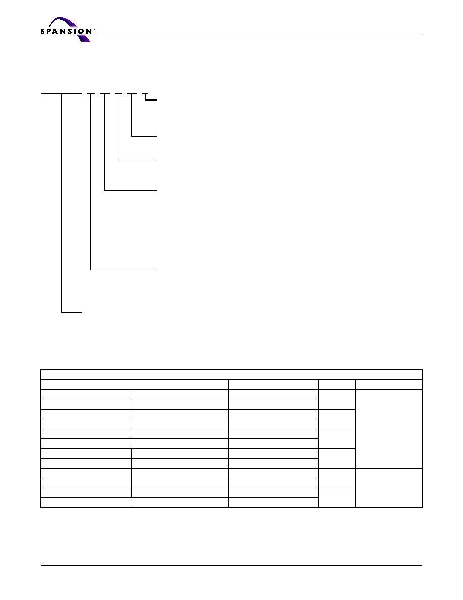
Logic Symbol
22
16 or 8
DQ15≠DQ0
(A-1)
A21≠A0
CE#
OE#
WE#
RESET#
BYTE#
RY/BY#
WP#/ACC
8
S29JL064H
S29JL064HA1 March 26, 2004
P r e l i m i n a r y
Ordering Information
The order number (Valid Combination) is formed by the following:
Valid Combinations list configurations planned to be supported in volume for this device. Consult your local sales office to con-
firm availability of specific valid combinations and to check on newly released combinations.
Note:Listed TSOP part numbers describe products based on Copper (Cu) leadframes. Contact your local sales office for
products based on Alloy-42 leadframes.
S29JL064H
55
TA
I
00
0
PACKING TYPE
0
= Tray
2
= 7- inch Tape and Reel
3
= 13-inch Tape and Reel
MODEL NUMBER (ADDITIONAL ORDERING OPTIONS)
00
= Standard Configuration
TEMPERATURE RANGE
I =
Industrial
(≠40∞C to +85∞C)
N = Extended
(≠40∞C to +125∞C)
PACKAGE TYPE
TA
= 48-Pin Thin Small Outline Package (TSOP, TS048)
Not Lead (Pb)-free, Copper Leadframe
TF
= 48-Pin Thin Small Outline Package (TSOP, TS048)
Lead (Pb)-Free, Copper Leadframe, Tin plating
BA
= 63-ball Ball Grid Array (BGA, FBE063)
0.8 mm pitch, 12 x 11 mm Package
Not Lead (Pb)-Free
BF
= 63-ball Ball Grid Array (BGA, FBE063)
0.8 mm pitch, 12 x 11 mm Package
Lead (Pb)-Free
SPEED OPTION
55
= 55 ns
60
= 60 ns
70
= 70 ns
90
= 90 ns
DEVICE FAMILY
S29JL064H
3.0 Volt-only, 64 Megabit (4 M x 16-Bit/8 M x 8-Bit) Simultaneous Read/Write Flash Memory
Manufactured on 130 nm process technology
Valid Combinations for TSOP Packages
Order Number
Package Markings
Package
Speed
Temperature Range
S29JL064H55TAI00
S29JL064H55TAI00
Not Lead (Pb)- Free
55
-40≠85 ∞C
S29JL064H55TFI00
S29JL064H55TFI00
Lead (Pb)- Free
S29JL064H60TAI00
S29JL064H60TAI00
Not Lead (Pb)- Free
60
S29JL064H60TFI00
S29JL064H60TFI00
Lead (Pb)- Free
S29JL064H70TAI00
S29JL064H70TAI00
Not Lead (Pb)- Free
70
S29JL064H70TFI00
S29JL064H70TFI00
Lead (Pb)- Free
S29JL064H90TAI00
S29JL064H90TAI00
Not Lead (Pb)- Free
90
S29JL064H90TFI00
S29JL064H90TFI00
Lead (Pb)- Free
S29JL064H70TAN00
S29JL064H70TAN00
Not Lead (Pb)- Free
70
-40≠125 ∞C
S29JL064H70TFN00
S29JL064H70TFN00
Lead (Pb)- Free
S29JL064H90TAN00
S29JL064H90TAN00
Not Lead (Pb)- Free
90
S29JL064H90TFN00
S29JL064H90TFN00
Lead (Pb)- Free
March 26, 2004 S29JL064HA1
S29JL064H
9
P r e l i m i n a r y
Valid Combinations for BGA Packages
Order Number
Package Markings
Package
Speed
Temperature Range
S29JL064H55BAI00
JL064H55BAI00
Not Lead (Pb)- Free
55
-40≠85 ∞C
S29JL064H55BFI00
JL064H55BFI00
Lead (Pb)- Free
S29JL064H60BAI00
JL064H60BAI00
Not Lead (Pb)- Free
60
S29JL064H60BFI00
JL064H60BFI00
Lead (Pb)- Free
S29JL064H70BAI00
JL064H70BAI00
Not Lead (Pb)- Free
70
S29JL064H70BFI00
JL064H70BFI00
Lead (Pb)- Free
S29JL064H90BAI00
JL064H90BAI00
Not Lead (Pb)- Free
90
S29JL064H90BFI00
JL064H90BFI00
Lead (Pb)- Free

10
S29JL064H
S29JL064HA1 March 26, 2004
P r e l i m i n a r y
Device Bus Operations
This section describes the requirements and use of the device bus operations,
which are initiated through the internal command register. The command register
itself does not occupy any addressable memory location. The register is a latch
used to store the commands, along with the address and data information
needed to execute the command. The contents of the register serve as inputs to
the internal state machine. The state machine outputs dictate the function of the
device. Table
1
lists the device bus operations, the inputs and control levels they
require, and the resulting output. The following subsections describe each of
these operations in further detail.
Table 1. S29JL064H Device Bus Operations
Legend: L = Logic Low = V
IL
, H = Logic High = V
IH
, V
ID
= 11.5≠12.5 V, V
HH
= 9.0 ± 0.5 V, X = Don't Care, SA = Sector
Address, A
IN
= Address In, D
IN
= Data In, D
OUT
= Data Out
Notes:
1. Addresses are A21:A0 in word mode (BYTE# = V
IH
), A21:A-1 in byte mode (BYTE# = V
IL
).
2. The sector protect and sector unprotect functions may also be implemented via programming equipment. See
the "Sector/Sector Block Protection and Unprotection" section.
3. If WP#/ACC = V
IL
, sectors 0, 1, 140, and 141 remain protected. If WP#/ACC = V
IH
, protection on sectors 0, 1, 140,
and 141 depends on whether they were last protected or unprotected using the method described in "Sector/Sector
Block Protection and Unprotection". If WP#/ACC = V
HH
, all sectors will be unprotected.
Operation
CE#
OE# WE# RESET# WP#/ACC
Addresses
(Note 2)
DQ15≠DQ8
DQ7≠
DQ0
BYTE#
= V
IH
BYTE#
= V
IL
Read
L
L
H
H
L/H
A
IN
D
OUT
DQ14≠DQ8 = High-
Z, DQ15 = A-1
D
OUT
Write
L
H
L
H
(Note 3)
A
IN
D
IN
D
IN
Standby
V
CC
±
0.3 V
X
X
V
CC
±
0.3 V
L/H
X
High-Z
High-Z
High-Z
Output Disable
L
H
H
H
L/H
X
High-Z
High-Z
High-Z
Reset
X
X
X
L
L/H
X
High-Z
High-Z
High-Z
Sector Protect (Note 2)
L
H
L
V
ID
L/H
SA, A6 = L,
A1 = H, A0 = L
X
X
D
IN
Sector Unprotect (Note 2)
L
H
L
V
ID
(Note 3)
SA, A6 = H,
A1 = H, A0 = L
X
X
D
IN
Temporary Sector
Unprotect
X
X
X
V
ID
(Note 3)
A
IN
D
IN
High-Z
D
IN

March 26, 2004 S29JL064HA1
S29JL064H
11
P r e l i m i n a r y
Word/Byte Configuration
The BYTE# pin controls whether the device data I/O pins operate in the byte or
word configuration. If the BYTE# pin is set at logic `1', the device is in word con-
figuration, DQ15≠DQ0 are active and controlled by CE# and OE#.
If the BYTE# pin is set at logic `0', the device is in byte configuration, and only
data I/O pins DQ7≠DQ0 are active and controlled by CE# and OE#. The data I/
O pins DQ14≠DQ8 are tri-stated, and the DQ15 pin is used as an input for the
LSB (A-1) address function.
Requirements for Reading Array Data
To read array data from the outputs, the system must drive the CE# and OE#
pins to V
IL
. CE# is the power control and selects the device. OE# is the output
control and gates array data to the output pins. WE# should remain at V
IH
. The
BYTE# pin determines whether the device outputs array data in words or bytes.
The internal state machine is set for reading array data upon device power-up,
or after a hardware reset. This ensures that no spurious alteration of the memory
content occurs during the power transition. No command is necessary in this
mode to obtain array data. Standard microprocessor read cycles that assert valid
addresses on the device address inputs produce valid data on the device data
outputs. Each bank remains enabled for read access until the command register
contents are altered.
Refer to the AC Read-Only Operations table for timing specifications and to 14 for
the timing diagram. I
CC1
in the DC Characteristics table represents the active cur-
rent specification for reading array data.
Writing Commands/Command Sequences
To write a command or command sequence (which includes programming data
to the device and erasing sectors of memory), the system must drive WE# and
CE# to V
IL
, and OE# to V
IH
.
For program operations, the BYTE# pin determines whether the device accepts
program data in bytes or words. Refer to "Word/Byte Configuration" for more
information.
The device features an Unlock Bypass mode to facilitate faster programming.
Once a bank enters the Unlock Bypass mode, only two write cycles are required
to program a word or byte, instead of four. The "Byte/Word Program Command
Sequence" section has details on programming data to the device using both
standard and Unlock Bypass command sequences.
An erase operation can erase one sector, multiple sectors, or the entire device.
Table
3
indicates the address space that each sector occupies. Similarly, a "sector
address" is the address bits required to uniquely select a sector. The "Command
Definitions" section has details on erasing a sector or the entire chip, or suspend-
ing/resuming the erase operation.
The device address space is divided into four banks. A "bank address" is the ad-
dress bits required to uniquely select a bank.
I
CC2
in the DC Characteristics table represents the active current specification for
the write mode. The AC Characteristics section contains timing specification ta-
bles and timing diagrams for write operations.

12
S29JL064H
S29JL064HA1 March 26, 2004
P r e l i m i n a r y
Accelerated Program Operation
The device offers accelerated program operations through the ACC function. This
is one of two functions provided by the WP#/ACC pin. This function is primarily
intended to allow faster manufacturing throughput at the factory.
If the system asserts V
HH
on this pin, the device automatically enters the afore-
mentioned Unlock Bypass mode, temporarily unprotects any protected sectors,
and uses the higher voltage on the pin to reduce the time required for program
operations. The system would use a two-cycle program command sequence as
required by the Unlock Bypass mode. Removing V
HH
from the WP#/ACC pin re-
turns the device to normal operation. Note that V
HH
must not be asserted on
WP#/ACC for operations other than accelerated programming, or device damage
may result. In addition, the WP#/ACC pin must not be left floating or uncon-
nected; inconsistent behavior of the device may result. See "Write Protect
(WP#)" on page 21. for related information.
Autoselect Functions
If the system writes the autoselect command sequence, the device enters the au-
toselect mode. The system can then read autoselect codes from the internal
register (which is separate from the memory array) on DQ15≠DQ0. Standard
read cycle timings apply in this mode. Refer to the Autoselect Mode and Autose-
lect Command Sequence sections for more information.
Simultaneous Read/Write Operations with Zero Latency
This device is capable of reading data from one bank of memory while program-
ming or erasing in the other bank of memory. An erase operation may also be
suspended to read from or program to another location within the same bank (ex-
cept the sector being erased).
Figure 21
shows how read and write cycles may be
initiated for simultaneous operation with zero latency. I
CC6
and I
CC7
in the DC
Characteristics table represent the current specifications for read-while-program
and read-while-erase, respectively.

March 26, 2004 S29JL064HA1
S29JL064H
13
P r e l i m i n a r y
Standby Mode
When the system is not reading or writing to the device, it can place the device
in the standby mode. In this mode, current consumption is greatly reduced, and
the outputs are placed in the high impedance state, independent of the OE#
input.
The device enters the CMOS standby mode when the CE# and RESET# pins are
both held at V
CC
± 0.3 V. (Note that this is a more restricted voltage range than
V
IH
.) If CE# and RESET# are held at V
IH
, but not within V
CC
± 0.3 V, the device
will be in the standby mode, but the standby current will be greater. The device
requires standard access time (t
CE
) for read access when the device is in either
of these standby modes, before it is ready to read data.
If the device is deselected during erasure or programming, the device draws ac-
tive current until the operation is completed.
I
CC3
in the DC Characteristics table represents the standby current specification.
Automatic Sleep Mode
The automatic sleep mode minimizes Flash device energy consumption. The de-
vice automatically enables this mode when addresses remain stable for t
ACC
+
30 ns. The automatic sleep mode is independent of the CE#, WE#, and OE# con-
trol signals. Standard address access timings provide new data when addresses
are changed. While in sleep mode, output data is latched and always available to
the system. I
CC5
in the DC Characteristics table represents the automatic sleep
mode current specification.
RESET#: Hardware Reset Pin
The RESET# pin provides a hardware method of resetting the device to reading
array data. When the RESET# pin is driven low for at least a period of t
RP
, the
device immediately terminates any operation in progress, tristates all output
pins, and ignores all read/write commands for the duration of the RESET# pulse.
The device also resets the internal state machine to reading array data. The op-
eration that was interrupted should be reinitiated once the device is ready to
accept another command sequence, to ensure data integrity.
Current is reduced for the duration of the RESET# pulse. When RESET# is held
at V
SS
±0.3 V, the device draws CMOS standby current (I
CC4
). If RESET# is held
at V
IL
but not within V
SS
±0.3 V, the standby current will be greater.
The RESET# pin may be tied to the system reset circuitry. A system reset would
thus also reset the Flash memory, enabling the system to read the boot-up firm-
ware from the Flash memory.
If RESET# is asserted during a program or erase operation, the RY/BY# pin re-
mains a "0" (busy) until the internal reset operation is complete, which requires
a time of t
READY
(during Embedded Algorithms). The system can thus monitor RY/
BY# to determine whether the reset operation is complete. If RESET# is asserted
when a program or erase operation is not executing (RY/BY# pin is "1"), the reset
operation is completed within a time of t
READY
(not during Embedded Algorithms).
The system can read data t
RH
after the RESET# pin returns to V
IH
.
Refer to the AC Characteristics tables for RESET# parameters and to 15 for the
timing diagram.

14
S29JL064H
S29JL064HA1 March 26, 2004
P r e l i m i n a r y
Output Disable Mode
When the OE# input is at V
IH
, output from the device is disabled. The output pins
are placed in the high impedance state.

March 26, 2004 S29JL064HA1
S29JL064H
15
P r e l i m i n a r y
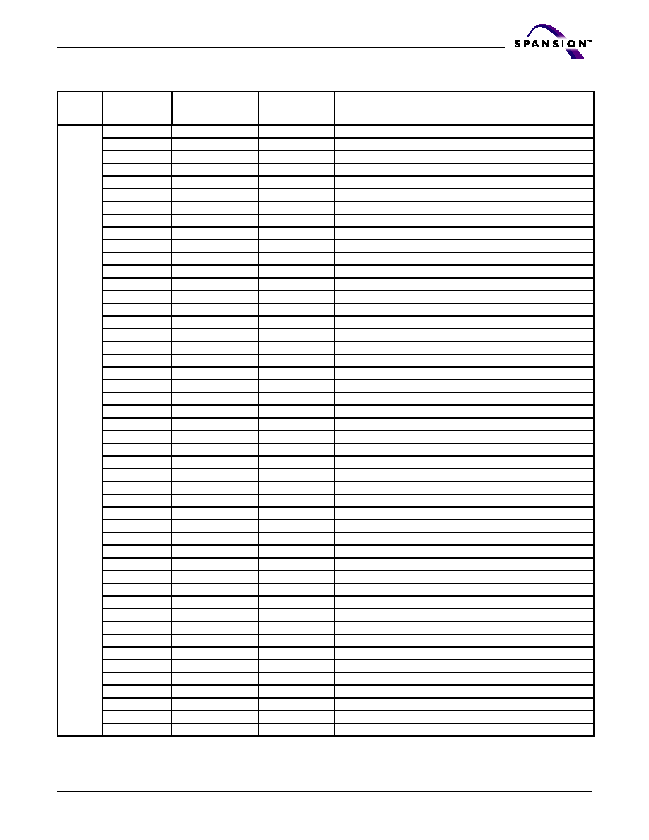
Table 2. S29JL064H Sector Architecture
Bank
Sector
Sector Address
A21≠A12
Sector Size
(Kbytes/
Kwords)
(x8)
Address Range
(x16)
Address Range
Bank 1
SA0
0000000000
8/4
000000h≠001FFFh
00000h≠00FFFh
SA1
0000000001
8/4
002000h≠003FFFh
01000h≠01FFFh
SA2
0000000010
8/4
004000h≠005FFFh
02000h≠02FFFh
SA3
0000000011
8/4
006000h≠007FFFh
03000h≠03FFFh
SA4
0000000100
8/4
008000h≠009FFFh
04000h≠04FFFh
SA5
0000000101
8/4
00A000h≠00BFFFh
05000h≠05FFFh
SA6
0000000110
8/4
00C000h≠00DFFFh
06000h≠06FFFh
SA7
0000000111
8/4
00E000h≠00FFFFh
07000h≠07FFFh
SA8
0000001xxx
64/32
010000h≠01FFFFh
08000h≠0FFFFh
SA9
0000010xxx
64/32
020000h≠02FFFFh
10000h≠17FFFh
SA10
0000011xxx
64/32
030000h≠03FFFFh
18000h≠1FFFFh
SA11
0000100xxx
64/32
040000h≠04FFFFh
20000h≠27FFFh
SA12
0000101xxx
64/32
050000h≠05FFFFh
28000h≠2FFFFh
SA13
0000110xxx
64/32
060000h≠06FFFFh
30000h≠37FFFh
SA14
0000111xxx
64/32
070000h≠07FFFFh
38000h≠3FFFFh
SA15
0001000xxx
64/32
080000h≠08FFFFh
40000h≠47FFFh
SA16
0001001xxx
64/32
090000h≠09FFFFh
48000h≠4FFFFh
SA17
0001010xxx
64/32
0A0000h≠0AFFFFh
50000h≠57FFFh
SA18
0001011xxx
64/32
0B0000h≠0BFFFFh
58000h≠5FFFFh
SA19
0001100xxx
64/32
0C0000h≠0CFFFFh
60000h≠67FFFh
SA20
0001101xxx
64/32
0D0000h≠0DFFFFh
68000h≠6FFFFh
SA21
0001110xxx
64/32
0E0000h≠0EFFFFh
70000h≠77FFFh
SA22
0001111xxx
64/32
0F0000h≠0FFFFFh
78000h≠7FFFFh

16
S29JL064H
S29JL064HA1 March 26, 2004
P r e l i m i n a r y
Bank 2
SA23
0010000xxx
64/32
100000h≠10FFFFh
80000h≠87FFFh
SA24
0010001xxx
64/32
110000h≠11FFFFh
88000h≠8FFFFh
SA25
0010010xxx
64/32
120000h≠12FFFFh
90000h≠97FFFh
SA26
0010011xxx
64/32
130000h≠13FFFFh
98000h≠9FFFFh
SA27
0010100xxx
64/32
140000h≠14FFFFh
A0000h≠A7FFFh
SA28
0010101xxx
64/32
150000h≠15FFFFh
A8000h≠AFFFFh
SA29
0010110xxx
64/32
160000h≠16FFFFh
B0000h≠B7FFFh
SA30
0010111xxx
64/32
170000h≠17FFFFh
B8000h≠BFFFFh
SA31
0011000xxx
64/32
180000h≠18FFFFh
C0000h≠C7FFFh
SA32
0011001xxx
64/32
190000h≠19FFFFh
C8000h≠CFFFFh
SA33
0011010xxx
64/32
1A0000h≠1AFFFFh
D0000h≠D7FFFh
SA34
0011011xxx
64/32
1B0000h≠1BFFFFh
D8000h≠DFFFFh
SA35
0011000xxx
64/32
1C0000h≠1CFFFFh
E0000h≠E7FFFh
SA36
0011101xxx
64/32
1D0000h≠1DFFFFh
E8000h≠EFFFFh
SA37
0011110xxx
64/32
1E0000h≠1EFFFFh
F0000h≠F7FFFh
SA38
0011111xxx
64/32
1F0000h≠1FFFFFh
F8000h≠FFFFFh
SA39
0100000xxx
64/32
200000h≠20FFFFh
100000h≠107FFFh
SA40
0100001xxx
64/32
210000h≠21FFFFh
108000h≠10FFFFh
SA41
0100010xxx
64/32
220000h≠22FFFFh
110000h≠117FFFh
SA42
0101011xxx
64/32
230000h≠23FFFFh
118000h≠11FFFFh
SA43
0100100xxx
64/32
240000h≠24FFFFh
120000h≠127FFFh
SA44
0100101xxx
64/32
250000h≠25FFFFh
128000h≠12FFFFh
SA45
0100110xxx
64/32
260000h≠26FFFFh
130000h≠137FFFh
SA46
0100111xxx
64/32
270000h≠27FFFFh
138000h≠13FFFFh
SA47
0101000xxx
64/32
280000h≠28FFFFh
140000h≠147FFFh
SA48
0101001xxx
64/32
290000h≠29FFFFh
148000h≠14FFFFh
SA49
0101010xxx
64/32
2A0000h≠2AFFFFh
150000h≠157FFFh
SA50
0101011xxx
64/32
2B0000h≠2BFFFFh
158000h≠15FFFFh
SA51
0101100xxx
64/32
2C0000h≠2CFFFFh
160000h≠167FFFh
SA52
0101101xxx
64/32
2D0000h≠2DFFFFh
168000h≠16FFFFh
SA53
0101110xxx
64/32
2E0000h≠2EFFFFh
170000h≠177FFFh
SA54
0101111xxx
64/32
2F0000h≠2FFFFFh
178000h≠17FFFFh
SA55
0110000xxx
64/32
300000h≠30FFFFh
180000h≠187FFFh
SA56
0110001xxx
64/32
310000h≠31FFFFh
188000h≠18FFFFh
SA57
0110010xxx
64/32
320000h≠32FFFFh
190000h≠197FFFh
SA58
0110011xxx
64/32
330000h≠33FFFFh
198000h≠19FFFFh
SA59
0110100xxx
64/32
340000h≠34FFFFh
1A0000h≠1A7FFFh
SA60
0110101xxx
64/32
350000h≠35FFFFh
1A8000h≠1AFFFFh
SA61
0110110xxx
64/32
360000h≠36FFFFh
1B0000h≠1B7FFFh
SA62
0110111xxx
64/32
370000h≠37FFFFh
1B8000h≠1BFFFFh
SA63
0111000xxx
64/32
380000h≠38FFFFh
1C0000h≠1C7FFFh
SA64
0111001xxx
64/32
390000h≠39FFFFh
1C8000h≠1CFFFFh
SA65
0111010xxx
64/32
3A0000h≠3AFFFFh
1D0000h≠1D7FFFh
SA66
0111011xxx
64/32
3B0000h≠3BFFFFh
1D8000h≠1DFFFFh
SA67
0111100xxx
64/32
3C0000h≠3CFFFFh
1E0000h≠1E7FFFh
SA68
0111101xxx
64/32
3D0000h≠3DFFFFh
1E8000h≠1EFFFFh
SA69
0111110xxx
64/32
3E0000h≠3EFFFFh
1F0000h≠1F7FFFh
SA70
0111111xxx
64/32
3F0000h≠3FFFFFh
1F8000h≠1FFFFFh
Table 2. S29JL064H Sector Architecture (Continued)
Bank
Sector
Sector Address
A21≠A12
Sector Size
(Kbytes/
Kwords)
(x8)
Address Range
(x16)
Address Range
March 26, 2004 S29JL064HA1
S29JL064H
17
P r e l i m i n a r y
Bank 3
SA71
1000000xxx
64/32
400000h≠40FFFFh
200000h≠207FFFh
SA72
1000001xxx
64/32
410000h≠41FFFFh
208000h≠20FFFFh
SA73
1000010xxx
64/32
420000h≠42FFFFh
210000h≠217FFFh
SA74
1000011xxx
64/32
430000h≠43FFFFh
218000h≠21FFFFh
SA75
1000100xxx
64/32
440000h≠44FFFFh
220000h≠227FFFh
SA76
1000101xxx
64/32
450000h≠45FFFFh
228000h≠22FFFFh
SA77
1000110xxx
64/32
460000h≠46FFFFh
230000h≠237FFFh
SA78
1000111xxx
64/32
470000h≠47FFFFh
238000h≠23FFFFh
SA79
1001000xxx
64/32
480000h≠48FFFFh
240000h≠247FFFh
SA80
1001001xxx
64/32
490000h≠49FFFFh
248000h≠24FFFFh
SA81
1001010xxx
64/32
4A0000h≠4AFFFFh
250000h≠257FFFh
SA82
1001011xxx
64/32
4B0000h≠4BFFFFh
258000h≠25FFFFh
SA83
1001100xxx
64/32
4C0000h≠4CFFFFh
260000h≠267FFFh
SA84
1001101xxx
64/32
4D0000h≠4DFFFFh
268000h≠26FFFFh
SA85
1001110xxx
64/32
4E0000h≠4EFFFFh
270000h≠277FFFh
SA86
1001111xxx
64/32
4F0000h≠4FFFFFh
278000h≠27FFFFh
SA87
1010000xxx
64/32
500000h≠50FFFFh
280000h≠28FFFFh
SA88
1010001xxx
64/32
510000h≠51FFFFh
288000h≠28FFFFh
SA89
1010010xxx
64/32
520000h≠52FFFFh
290000h≠297FFFh
SA90
1010011xxx
64/32
530000h≠53FFFFh
298000h≠29FFFFh
SA91
1010100xxx
64/32
540000h≠54FFFFh
2A0000h≠2A7FFFh
SA92
1010101xxx
64/32
550000h≠55FFFFh
2A8000h≠2AFFFFh
SA93
1010110xxx
64/32
560000h≠56FFFFh
2B0000h≠2B7FFFh
SA94
1010111xxx
64/32
570000h≠57FFFFh
2B8000h≠2BFFFFh
SA95
1011000xxx
64/32
580000h≠58FFFFh
2C0000h≠2C7FFFh
SA96
1011001xxx
64/32
590000h≠59FFFFh
2C8000h≠2CFFFFh
SA97
1011010xxx
64/32
5A0000h≠5AFFFFh
2D0000h≠2D7FFFh
SA98
1011011xxx
64/32
5B0000h≠5BFFFFh
2D8000h≠2DFFFFh
SA99
1011100xxx
64/32
5C0000h≠5CFFFFh
2E0000h≠2E7FFFh
SA100
1011101xxx
64/32
5D0000h≠5DFFFFh
2E8000h≠2EFFFFh
SA101
1011110xxx
64/32
5E0000h≠5EFFFFh
2F0000h≠2FFFFFh
SA102
1011111xxx
64/32
5F0000h≠5FFFFFh
2F8000h≠2FFFFFh
SA103
1100000xxx
64/32
600000h≠60FFFFh
300000h≠307FFFh
SA104
1100001xxx
64/32
610000h≠61FFFFh
308000h≠30FFFFh
SA105
1100010xxx
64/32
620000h≠62FFFFh
310000h≠317FFFh
SA106
1100011xxx
64/32
630000h≠63FFFFh
318000h≠31FFFFh
SA107
1100100xxx
64/32
640000h≠64FFFFh
320000h≠327FFFh
SA108
1100101xxx
64/32
650000h≠65FFFFh
328000h≠32FFFFh
SA109
1100110xxx
64/32
660000h≠66FFFFh
330000h≠337FFFh
SA110
1100111xxx
64/32
670000h≠67FFFFh
338000h≠33FFFFh
SA111
1101000xxx
64/32
680000h≠68FFFFh
340000h≠347FFFh
SA112
1101001xxx
64/32
690000h≠69FFFFh
348000h≠34FFFFh
SA113
1101010xxx
64/32
6A0000h≠6AFFFFh
350000h≠357FFFh
SA114
1101011xxx
64/32
6B0000h≠6BFFFFh
358000h≠35FFFFh
SA115
1101100xxx
64/32
6C0000h≠6CFFFFh
360000h≠367FFFh
SA116
1101101xxx
64/32
6D0000h≠6DFFFFh
368000h≠36FFFFh
SA117
1101110xxx
64/32
6E0000h≠6EFFFFh
370000h≠377FFFh
SA118
1101111xxx
64/32
6F0000h≠6FFFFFh
378000h≠37FFFFh
Table 2. S29JL064H Sector Architecture (Continued)
Bank
Sector
Sector Address
A21≠A12
Sector Size
(Kbytes/
Kwords)
(x8)
Address Range
(x16)
Address Range

18
S29JL064H
S29JL064HA1 March 26, 2004
P r e l i m i n a r y
Note: The address range is A21:A-1 in byte mode (BYTE#=V
IL
) or A21:A0 in word mode (BYTE#=V
IH
).
Table 3. Bank Address
Table 4. SecSi
TM
Sector Addresses
Autoselect Mode
The autoselect mode provides manufacturer and device identification, and sector
protection verification, through identifier codes output on DQ7≠DQ0. This mode
is primarily intended for programming equipment to automatically match a device
to be programmed with its corresponding programming algorithm. However, the
autoselect codes can also be accessed in-system through the command register.
Bank 4
SA119
1110000xxx
64/32
700000h≠70FFFFh
380000h≠387FFFh
SA120
1110001xxx
64/32
710000h≠71FFFFh
388000h≠38FFFFh
SA121
1110010xxx
64/32
720000h≠72FFFFh
390000h≠397FFFh
SA122
1110011xxx
64/32
730000h≠73FFFFh
398000h≠39FFFFh
SA123
1110100xxx
64/32
740000h≠74FFFFh
3A0000h≠3A7FFFh
SA124
1110101xxx
64/32
750000h≠75FFFFh
3A8000h≠3AFFFFh
SA125
1110110xxx
64/32
760000h≠76FFFFh
3B0000h≠3B7FFFh
SA126
1110111xxx
64/32
770000h≠77FFFFh
3B8000h≠3BFFFFh
SA127
1111000xxx
64/32
780000h≠78FFFFh
3C0000h≠3C7FFFh
SA128
1111001xxx
64/32
790000h≠79FFFFh
3C8000h≠3CFFFFh
SA129
1111010xxx
64/32
7A0000h≠7AFFFFh
3D0000h≠3D7FFFh
SA130
1111011xxx
64/32
7B0000h≠7BFFFFh
3D8000h≠3DFFFFh
SA131
1111100xxx
64/32
7C0000h≠7CFFFFh
3E0000h≠3E7FFFh
SA132
1111101xxx
64/32
7D0000h≠7DFFFFh
3E8000h≠3EFFFFh
SA133
1111110xxx
64/32
7E0000h≠7EFFFFh
3F0000h≠3F7FFFh
SA134
1111111000
8/4
7F0000h≠7F1FFFh
3F8000h≠3F8FFFh
SA135
1111111001
8/4
7F2000h≠7F3FFFh
3F9000h≠3F9FFFh
SA136
1111111010
8/4
7F4000h≠7F5FFFh
3FA000h≠3FAFFFh
SA137
1111111011
8/4
7F6000h≠7F7FFFh
3FB000h≠3FBFFFh
SA138
1111111100
8/4
7F8000h≠7F9FFFh
3FC000h≠3FCFFFh
SA139
1111111101
8/4
7FA000h≠7FBFFFh
3FD000h≠3FDFFFh
SA140
1111111110
8/4
7FC000h≠7FDFFFh
3FE000h≠3FEFFFh
SA141
1111111111
8/4
7FE000h≠7FFFFFh
3FF000h≠3FFFFFh
Bank
A21≠A19
1
000
2
001, 010, 011
3
100, 101, 110
4
111
Device
Sector Size
(x8)
Address Range
(x16)
Address Range
S29JL064H
256 bytes
000000h≠0000FFh
000000h≠00007Fh
Table 2. S29JL064H Sector Architecture (Continued)
Bank
Sector
Sector Address
A21≠A12
Sector Size
(Kbytes/
Kwords)
(x8)
Address Range
(x16)
Address Range
March 26, 2004 S29JL064HA1
S29JL064H
19
P r e l i m i n a r y
When using programming equipment, the autoselect mode requires
V
ID
on ad-
dress pin A9. Address pins must be as shown in Table
5
. In addition, when
verifying sector protection, the sector address must appear on the appropriate
highest order address bits (see Table
3
). Table
5
shows the remaining address
bits that are don't care. When all necessary bits have been set as required, the
programming equipment may then read the corresponding identifier code on
DQ7≠DQ0. However, the autoselect codes can also be accessed in-system
through the command register, for instances when the S29JL064 is erased or pro-
grammed in a system without access to high voltage on the A9 pin. The command
sequence is illustrated in Table
4
. Note that if a Bank Address (BA) on address
bits A21, A20, and A19 is asserted during the third write cycle of the autoselect
command, the host system can read autoselect data from that bank and then im-
mediately read array data from another bank, without exiting the autoselect
mode.
To access the autoselect codes in-system, the host system can issue the autose-
lect command via the command register, as shown in Table
4
. This method does
not require V
ID
. Refer to the Autoselect Command Sequence section for more
information.
Table 5. S29JL064H Autoselect Codes, (High Voltage Method)
Legend: L = Logic Low = V
IL
, H = Logic High = V
IH
, BA = Bank Address, SA = Sector Address, X = Don't care.
Sector/Sector Block Protection and Unprotection
(Note: For the following discussion, the term "sector" applies to both sectors and
sector blocks. A sector block consists of two or more adjacent sectors that are
protected or unprotected at the same time (see Table
6
).
The hardware sector protection feature disables both program and erase opera-
tions in any sector. The hardware sector unprotection feature re-enables both
program and erase operations in previously protected sectors. Sector protection/
unprotection can be implemented via two methods.
Description
CE# OE# WE#
A21
to
A12
A11
to
A10
A9
A8
to
A7
A6
A5
to
A4
A3
A2
A1
A0
DQ15 to DQ8
DQ7
to
DQ0
BYTE#
= V
IH
BYTE#
= V
IL
Manufacturer ID:
Spansion Products
L
L
H
BA
X
V
ID
X
L
X
L
L
L
L
X
X
01h
Dev
i
c
e
ID
Read Cycle 1
L
L
H
BA
X
V
ID
X
L
X
L
L
L
H
22h
X
7Eh
Read Cycle 2
L
H
H
H
L
22h
02h
Read Cycle 3
L
H
H
H
H
22h
01h
Sector Protection
Verification
L
L
H
SA
X
V
ID
X
L
X
L
L
H
L
X
X
01h (protected),
00h (unprotected)
SecSi Indicator Bit
(DQ6, DQ7)
L
L
H
BA
X
V
ID
X
L
X
L
L
H
H
X
X
80h (factory locked),
40h (customer
locked), 00h (not
factory/customer
locked)

20
S29JL064H
S29JL064HA1 March 26, 2004
P r e l i m i n a r y
Table 6. S29JL064H Boot Sector/Sector Block
Addresses for Protection/Unprotection
Sector
A21≠A12
Sector/
Sector Block Size
SA0
0000000000
8 Kbytes
SA1
0000000001
8 Kbytes
SA2
0000000010
8 Kbytes
SA3
0000000011
8 Kbytes
SA4
0000000100
8 Kbytes
SA5
0000000101
8 Kbytes
SA6
0000000110
8 Kbytes
SA7
0000000111
8 Kbytes
SA8≠SA10
0000001XXX,
0000010XXX,
0000011XXX,
192 (3x64) Kbytes
SA11≠SA14
00001XXXXX
256 (4x64) Kbytes
SA15≠SA18
00010XXXXX
256 (4x64) Kbytes
SA19≠SA22
00011XXXXX
256 (4x64) Kbytes
SA23≠SA26
00100XXXXX
256 (4x64) Kbytes
SA27-SA30
00101XXXXX
256 (4x64) Kbytes
SA31-SA34
00110XXXXX
256 (4x64) Kbytes
SA35-SA38
00111XXXXX
256 (4x64) Kbytes
SA39-SA42
01000XXXXX
256 (4x64) Kbytes
SA43-SA46
01001XXXXX
256 (4x64) Kbytes
SA47-SA50
01010XXXXX
256 (4x64) Kbytes
SA51-SA54
01011XXXXX
256 (4x64) Kbytes
SA55≠SA58
01100XXXXX
256 (4x64) Kbytes
SA59≠SA62
01101XXXXX
256 (4x64) Kbytes
SA63≠SA66
01110XXXXX
256 (4x64) Kbytes
SA67≠SA70
01111XXXXX
256 (4x64) Kbytes
SA71≠SA74
10000XXXXX
256 (4x64) Kbytes
SA75≠SA78
10001XXXXX
256 (4x64) Kbytes
SA79≠SA82
10010XXXXX
256 (4x64) Kbytes
SA83≠SA86
10011XXXXX
256 (4x64) Kbytes
SA87≠SA90
10100XXXXX
256 (4x64) Kbytes
SA91≠SA94
10101XXXXX
256 (4x64) Kbytes
SA95≠SA98
10110XXXXX
256 (4x64) Kbytes
SA99≠SA102
10111XXXXX
256 (4x64) Kbytes
SA103≠SA106
11000XXXXX
256 (4x64) Kbytes
SA107≠SA110
11001XXXXX
256 (4x64) Kbytes
SA111≠SA114
11010XXXXX
256 (4x64) Kbytes
SA115≠SA118
11011XXXXX
256 (4x64) Kbytes
SA119≠SA122
11100XXXXX
256 (4x64) Kbytes
SA123≠SA126
11101XXXXX
256 (4x64) Kbytes
SA127≠SA130
11110XXXXX
256 (4x64) Kbytes
SA131≠SA133
1111100XXX,
1111101XXX,
1111110XXX
192 (3x64) Kbytes
SA134
1111111000
8 Kbytes
SA135
1111111001
8 Kbytes
SA136
1111111010
8 Kbytes
SA137
1111111011
8 Kbytes
SA138
1111111100
8 Kbytes
SA139
1111111101
8 Kbytes
SA140
1111111110
8 Kbytes
SA141
1111111111
8 Kbytes
Sector
A21≠A12
Sector/
Sector Block Size
March 26, 2004 S29JL064HA1
S29JL064H
21
P r e l i m i n a r y
Sector protect/Sector Unprotect requires V
ID
on the RESET# pin only, and can be
implemented either in-system or via programming equipment.
Figure 2
shows
the algorithms and
Figure 26
shows the timing diagram. For sector unprotect, all
unprotected sectors must first be protected prior to the first sector unprotect
write cycle. Note that the sector unprotect algorithm unprotects all sectors in par-
allel. All previously protected sectors must be individually re-protected. To
change data in protected sectors efficiently, the temporary sector unprotect func-
tion is available. See
"Temporary Sector Unprotect"
.
The device is shipped with all sectors unprotected. Optional Spansion program-
ming service enable programming and protecting sectors at the factory prior to
shipping the device. Contact your local sales office for details.
It is possible to determine whether a sector is protected or unprotected. See the
Autoselect Mode section for details.
Write Protect (WP#)
The Write Protect function provides a hardware method of protecting without
using V
ID
. This function is one of two provided by the WP#/ACC pin.
If the system asserts V
IL
on the WP#/ACC pin, the device disables program and
erase functions in sectors 0, 1, 140, and 141, independently of whether those
sectors were protected or unprotected using the method described in "Sector/
Sector Block Protection and Unprotection".
If the system asserts V
IH
on the WP#/ACC pin, the device reverts to whether sec-
tors 0, 1, 140, and 141 were last set to be protected or unprotected. That is,
sector protection or unprotection for these sectors depends on whether they were
last protected or unprotected using the method described in "Sector/Sector Block
Protection and Unprotection".
Note that the WP#/ACC pin must not be left floating or unconnected; inconsistent
behavior of the device may result.
Table 7. WP#/ACC Modes
Temporary Sector Unprotect
(Note: For the following discussion, the term "sector" applies to both sectors and
sector blocks. A sector block consists of two or more adjacent sectors that are
protected or unprotected at the same time (see Table
6
).
This feature allows temporary unprotection of previously protected sectors to
change data in-system. The Temporary Sector Unprotect mode is activated by
setting the RESET# pin to
V
ID
. During this mode, formerly protected sectors can
be programmed or erased by selecting the sector addresses. Once V
ID
is removed
from the RESET# pin, all the previously protected sectors are protected again.
shows the algorithm, and 25 shows the timing diagrams, for this feature. If the
WP#/ACC pin is at V
IL
, sectors 0, 1, 140, and 141 will remain protected during
the Temporary sector Unprotect mode.
WP# Input Voltage
Device
Mode
V
IL
Disables programming and erasing in SA0, SA1, SA140, and SA141
V
IH
Enables programming and erasing in SA0, SA1, SA140, and SA141, dependent on
whether they were last protected or unprotected.
V
HH
Enables accelerated progamming (ACC). See "Accelerated Program Operation" on
page 12..
22
S29JL064H
S29JL064HA1 March 26, 2004
P r e l i m i n a r y
.
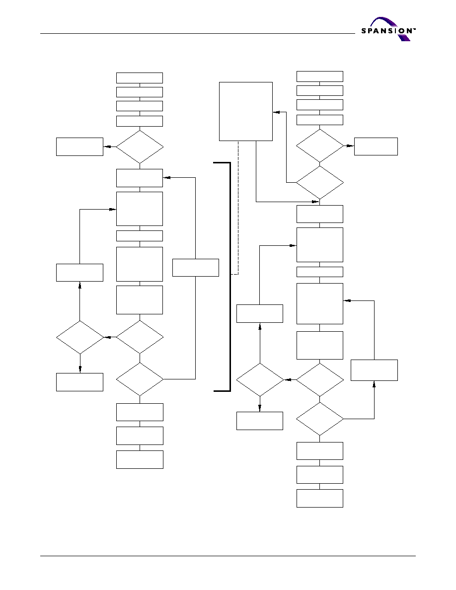
Figure 1. Temporary Sector Unprotect Operation
START
Perform Erase or
Program Operations
RESET# = V
IH
Temporary Sector
Unprotect Completed
(Note 2)
RESET# = V
ID
(Note 1)
Notes:
1. All protected sectors unprotected (If WP#/ACC =
V
IL
, sectors 0, 1, 140, and 141 will remain
protected).
2. All previously protected sectors are protected once
again.
March 26, 2004 S29JL064HA1
S29JL064H
23
P r e l i m i n a r y
Figure 2. In-System Sector Protect/Unprotect Algorithms
Sector Protect:
Write 60h to sector
address with
A6 = 0, A1 = 1,
A0 = 0
Set up sector
address
Wait 150 µs
Verify Sector
Protect: Write 40h
to sector address
with A6 = 0,
A1 = 1, A0 = 0
Read from
sector address
with A6 = 0,
A1 = 1, A0 = 0
START
PLSCNT = 1
RESET# = V
ID
Wait 1 ms
First Write
Cycle = 60h?
Data = 01h?
Remove V
ID
from RESET#
Write reset
command
Sector Protect
complete
Yes
Yes
No
PLSCNT
= 25?
Yes
Device failed
Increment
PLSCNT
Temporary Sector
Unprotect Mode
No
Sector Unprotect:
Write 60h to sector
address with
A6 = 1, A1 = 1,
A0 = 0
Set up first sector
address
Wait 15 ms
Verify Sector
Unprotect: Write
40h to sector
address with
A6 = 1, A1 = 1,
A0 = 0
Read from
sector address
with A6 = 1,
A1 = 1, A0 = 0
START
PLSCNT = 1
RESET# = V
ID
Wait 1 ms
Data = 00h?
Last sector
verified?
Remove V
ID
from RESET#
Write reset
command
Sector Unprotect
complete
Yes
No
PLSCNT
= 1000?
Yes
Device failed
Increment
PLSCNT
Temporary Sector
Unprotect Mode
No
All sectors
protected?
Yes
Protect all sectors:
The indicated portion
of the sector protect
algorithm must be
performed for all
unprotected sectors
prior to issuing the
first sector
unprotect address
Set up
next sector
address
No
Yes
No
Yes
No
No
Yes
No
Sector Protect
Algorithm
Sector Unprotect
Algorithm
First Write
Cycle = 60h?
Protect another
sector?
Reset
PLSCNT = 1

24
S29JL064H
S29JL064HA1 March 26, 2004
P r e l i m i n a r y
SecSiTM (Secured Silicon) Sector
Flash Memory Region
The SecSi (Secured Silicon) Sector feature provides a Flash memory region that
enables permanent part identification through an Electronic Serial Number
(ESN). The SecSi Sector is 256 bytes in length, and uses a SecSi Sector Indicator
Bit (DQ7) to indicate whether or not the SecSi Sector is locked when shipped from
the factory. This bit is permanently set at the factory and cannot be changed,
which prevents cloning of a factory locked part. This ensures the security of the
ESN once the product is shipped to the field.
The product is available with the SecSi Sector either factory locked or customer
lockable. The factory-locked version is always protected when shipped from the
factory, and has the SecSi (Secured Silicon) Sector Indicator Bit permanently set
to a "1." The customer-lockable version is shipped with the SecSi Sector unpro-
tected, allowing customers to utilize the that sector in any manner they choose.
The customer-lockable version has the SecSi (Secured Silicon) Sector Indicator
Bit permanently set to a "0." Thus, the SecSi Sector Indicator Bit prevents cus-
tomer-lockable devices from being used to replace devices that are factory
locked. The SecSi Customer Indicator Bit (DQ6) is permanently set to 1 if the part
has been customer locked, permanently set to 0 if the part has been factory
locked, and is 0 if customer lockable.
The system accesses the SecSi Sector Secure through a command sequence (see
"Enter SecSiTM Sector/Exit SecSi Sector Command Sequence"). After the system
has written the Enter SecSi Sector command sequence, it may read the SecSi
Sector by using the addresses normally occupied by the boot sectors. This mode
of operation continues until the system issues the Exit SecSi Sector command se-
quence, or until power is removed from the device. On power-up, or following a
hardware reset, the device reverts to sending commands to the first 256 bytes of
Sector 0. Note that the ACC function and unlock bypass modes are not available
when the SecSi Sector is enabled.
Factory Locked: SecSi Sector Programmed and Protected At the Factory
In a factory locked device, the SecSi Sector is protected when the device is
shipped from the factory. The SecSi Sector cannot be modified in any way. The
device is preprogrammed with both a random number and a secure ESN. The 8-
word random number is at addresses 000000h≠000007h in word mode (or
000000h≠00000Fh in byte mode). The secure ESN is programmed in the next 8
words at addresses 000008h≠00000Fh (or 000010h≠00001Fh in byte mode). The
device is available preprogrammed with one of the following:
A random, secure ESN only
Customer code through Spansion programming services
Both a random, secure ESN and customer code through Spansion program-
ming services
Contact an your local sales office for details on using Spansion programming
services.
Customer Lockable: SecSi Sector NOT Programmed or Protected At the Factory
If the security feature is not required, the SecSi Sector can be treated as an ad-
ditional Flash memory space. The SecSi Sector can be read any number of times,
but can be programmed and locked only once. Note that the accelerated pro-
gramming (ACC) and unlock bypass functions are not available when
programming the SecSi Sector.
March 26, 2004 S29JL064HA1
S29JL064H
25
P r e l i m i n a r y
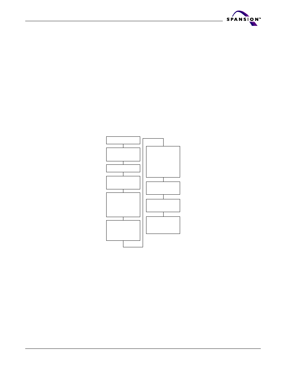
The SecSi Sector area can be protected using one of the following procedures:
Write the three-cycle Enter SecSi Sector Region command sequence, and
then follow the in-system sector protect algorithm as shown in
Figure 2
, ex-
cept that RESET# may be at either V
IH
or V
ID
. This allows in-system protec-
tion of the SecSi Sector Region without raising any device pin to a high
voltage. Note that this method is only applicable to the SecSi Sector.
To verify the protect/unprotect status of the SecSi Sector, follow the algo-
rithm shown in
Figure 3
.
Once the SecSi Sector is locked and verified, the system must write the Exit SecSi
Sector Region command sequence to return to reading and writing the remainder
of the array.
The SecSi Sector lock must be used with caution since, once locked, there is no
procedure available for unlocking the SecSi Sector area and none of the bits in
the SecSi Sector memory space can be modified in any way.
Figure 3. SecSi Sector Protect Verify
Hardware Data Protection
The command sequence requirement of unlock cycles for programming or erasing
provides data protection against inadvertent writes (refer to Table
4
for command
definitions). In addition, the following hardware data protection measures pre-
vent accidental erasure or programming, which might otherwise be caused by
spurious system level signals during V
CC
power-up and power-down transitions,
or from system noise.
Low V
CC
Write Inhibit
When V
CC
is less than V
LKO
, the device does not accept any write cycles. This pro-
tects data during V
CC
power-up and power-down. The command register and all
internal program/erase circuits are disabled, and the device resets to the read
Write 60h to
any address
Write 40h to SecSi
Sector address
with A6 = 0,
A1 = 1, A0 = 0
START
RESET# =
V
IH
or V
ID
Wait 1 ms
Read from SecSi
Sector address
with A6 = 0,
A1 = 1, A0 = 0
If data = 00h,
SecSi Sector is
unprotected.
If data = 01h,
SecSi Sector is
protected.
Remove V
IH
or V
ID
from RESET#
Write reset
command
SecSi Sector
Protect Verify
complete

26
S29JL064H
S29JL064HA1 March 26, 2004
P r e l i m i n a r y
mode. Subsequent writes are ignored until V
CC
is greater than V
LKO
. The system
must provide the proper signals to the control pins to prevent unintentional writes
when V
CC
is greater than V
LKO
.
Write Pulse "Glitch" Protection
Noise pulses of less than 5 ns (typical) on OE#, CE# or WE# do not initiate a write
cycle.
Logical Inhibit
Write cycles are inhibited by holding any one of OE# = V
IL
, CE# = V
IH
or WE# =
V
IH
. To initiate a write cycle, CE# and WE# must be a logical zero while OE# is a
logical one.
Power-Up Write Inhibit
If WE# = CE# = V
IL
and OE# = V
IH
during power up, the device does not accept
commands on the rising edge of WE#. The internal state machine is automatically
reset to the read mode on power-up.
Common Flash Memory Interface (CFI)
The Common Flash Interface (CFI) specification outlines device and host system
software interrogation handshake, which allows specific vendor-specified soft-
ware algorithms to be used for entire families of devices. Software support can
then be device-independent, JEDEC ID-independent, and forward- and back-
ward-compatible for the specified flash device families. Flash vendors can
standardize their existing interfaces for long-term compatibility.
This device enters the CFI Query mode when the system writes the CFI Query
command, 98h, to address 55h in word mode (or address AAh in byte mode), any
time the device is ready to read array data. The system can read CFI information
at the addresses given in Tables 1≠3. To terminate reading CFI data, the system
must write the reset command.The CFI Query mode is not accessible when the
device is executing an Embedded Program or embedded Erase algorithm.
The system can also write the CFI query command when the device is in the au-
toselect mode. The device enters the CFI query mode, and the system can read
CFI data at the addresses given in Tables 1≠3. The system must write the reset
command to reading array data.
For further information, please refer to the CFI Specification and CFI Publication
100. Contact your local sales office for copies of these documents.
March 26, 2004 S29JL064HA1
S29JL064H
27
P r e l i m i n a r y
Table 1. CFI Query Identification String
Table 8. System Interface String
Addresses
(Word Mode)
Addresses
(Byte Mode)
Data
Description
10h
11h
12h
20h
22h
24h
0051h
0052h
0059h
Query Unique ASCII string "QRY"
13h
14h
26h
28h
0002h
0000h
Primary OEM Command Set
15h
16h
2Ah
2Ch
0040h
0000h
Address for Primary Extended Table
17h
18h
2Eh
30h
0000h
0000h
Alternate OEM Command Set (00h = none exists)
19h
1Ah
32h
34h
0000h
0000h
Address for Alternate OEM Extended Table (00h = none exists)
Addresses
(Word Mode)
Addresses
(Byte Mode)
Data
Description
1Bh
36h
0027h
V
CC
Min. (write/erase)
D7≠D4: volt, D3≠D0: 100 millivolt
1Ch
38h
0036h
V
CC
Max. (write/erase)
D7≠D4: volt, D3≠D0: 100 millivolt
1Dh
3Ah
0000h
V
PP
Min. voltage (00h = no V
PP
pin present)
1Eh
3Ch
0000h
V
PP
Max. voltage (00h = no V
PP
pin present)
1Fh
3Eh
0003h
Typical timeout per single byte/word write 2
N
µs
20h
40h
0000h
Typical timeout for Min. size buffer write 2
N
µ
s (00h = not supported)
21h
42h
0009h
Typical timeout per individual block erase 2
N
ms
22h
44h
0000h
Typical timeout for full chip erase 2
N
ms (00h = not supported)
23h
46h
0005h
Max. timeout for byte/word write 2
N
times typical
24h
48h
0000h
Max. timeout for buffer write 2
N
times typical
25h
4Ah
0004h
Max. timeout per individual block erase 2
N
times typical
26h
4Ch
0000h
Max. timeout for full chip erase 2
N
times typical (00h = not supported)

28
S29JL064H
S29JL064HA1 March 26, 2004
P r e l i m i n a r y
Table 2. Device Geometry Definition
Addresses
(Word Mode)
Addresses
(Byte Mode)
Data
Description
27h
4Eh
0017h
Device Size = 2
N
byte
28h
29h
50h
52h
0002h
0000h
Flash Device Interface description (refer to CFI publication 100)
2Ah
2Bh
54h
56h
0000h
0000h
Max. number of byte in multi-byte write = 2
N
(00h = not supported)
2Ch
58h
0003h
Number of Erase Block Regions within device
2Dh
2Eh
2Fh
30h
5Ah
5Ch
5Eh
60h
0007h
0000h
0020h
0000h
Erase Block Region 1 Information
(refer to the CFI specification or CFI publication 100)
31h
32h
33h
34h
62h
64h
66h
68h
007Dh
0000h
0000h
0001h
Erase Block Region 2 Information
(refer to the CFI specification or CFI publication 100)
35h
36h
37h
38h
6Ah
6Ch
6Eh
70h
0007h
0000h
0020h
0000h
Erase Block Region 3 Information
(refer to the CFI specification or CFI publication 100)
39h
3Ah
3Bh
3Ch
72h
74h
76h
78h
0000h
0000h
0000h
0000h
Erase Block Region 4 Information
(refer to the CFI specification or CFI publication 100)
March 26, 2004 S29JL064HA1
S29JL064H
29
P r e l i m i n a r y
Table 3. Primary Vendor-Specific Extended Query
Addresses
(Word Mode)
Addresses
(Byte Mode)
Data
Description
40h
41h
42h
80h
82h
84h
0050h
0052h
0049h
Query-unique ASCII string "PRI"
43h
86h
0031h
Major version number, ASCII (reflects modifications to the silicon)
44h
88h
0033h
Minor version number, ASCII (reflects modifications to the CFI table)
45h
8Ah
000Ch
Address Sensitive Unlock (Bits 1-0)
0 = Required, 1 = Not Required
Silicon Revision Number (Bits 7-2)
46h
8Ch
0002h
Erase Suspend
0 = Not Supported, 1 = To Read Only, 2 = To Read & Write
47h
8Eh
0001h
Sector Protect
0 = Not Supported, X = Number of sectors in per group
48h
90h
0001h
Sector Temporary Unprotect
00 = Not Supported, 01 = Supported
49h
92h
0004h
Sector Protect/Unprotect scheme
01 =29F040 mode, 02 = 29F016 mode, 03 = 29F400, 04 = 29LV800
mode
4Ah
94h
0077h
Simultaneous Operation
00 = Not Supported, X = Number of Sectors (excluding Bank 1)
4Bh
96h
0000h
Burst Mode Type
00 = Not Supported, 01 = Supported
4Ch
98h
0000h
Page Mode Type
00 = Not Supported, 01 = 4 Word Page, 02 = 8 Word Page
4Dh
9Ah
0085h
ACC (Acceleration) Supply Minimum
00h = Not Supported, D7-D4: Volt, D3-D0: 100 mV
4Eh
9Ch
0095h
ACC (Acceleration) Supply Maximum
00h = Not Supported, D7-D4: Volt, D3-D0: 100 mV
4Fh
9Eh
0001h
Top/Bottom Boot Sector Flag
00h = Uniform device, 01h = 8 x 8 Kbyte Sectors, Top And Bottom
Boot with Write Protect, 02h = Bottom Boot Device, 03h = Top Boot
Device, 04h= Both Top and Bottom
50h
A0h
0001h
Program Suspend
0 = Not supported, 1 = Supported
57h
AEh
0004h
Bank Organization
00 = Data at 4Ah is zero, X = Number of Banks
58h
B0h
0017h
Bank 1 Region Information
X = Number of Sectors in Bank 1
59h
B2h
0030h
Bank 2 Region Information
X = Number of Sectors in Bank 2
5Ah
B4h
0030h
Bank 3 Region Information
X = Number of Sectors in Bank 3
5Bh
B6h
0017h
Bank 4 Region Information
X = Number of Sectors in Bank 4

30
S29JL064H
S29JL064HA1 March 26, 2004
P r e l i m i n a r y
Command Definitions
Writing specific address and data commands or sequences into the command
register initiates device operations. Table
4
defines the valid register command
sequences. Writing incorrect address and data values or writing them in the im-
proper sequence may place the device in an unknown state. A reset command is
then required to return the device to reading array data.
All addresses are latched on the falling edge of WE# or CE#, whichever happens
later. All data is latched on the rising edge of WE# or CE#, whichever happens
first. Refer to the AC Characteristics section for timing diagrams.
Reading Array Data
The device is automatically set to reading array data after device power-up. No
commands are required to retrieve data. Each bank is ready to read array data
after completing an Embedded Program or Embedded Erase algorithm.
After the device accepts an Erase Suspend command, the corresponding bank
enters the erase-suspend-read mode, after which the system can read data from
any non-erase-suspended sector within the same bank. The system can read
array data using the standard read timing, except that if it reads at an address
within erase-suspended sectors, the device outputs status data. After completing
a programming operation in the Erase Suspend mode, the system may once
again read array data with the same exception. See the Erase Suspend/Erase Re-
sume Commands section for more information.
The system must issue the reset command to return a bank to the read (or erase-
suspend-read) mode if DQ5 goes high during an active program or erase opera-
tion, or if the bank is in the autoselect mode. See the next section, Reset
Command, for more information.
See also Requirements for Reading Array Data in the Device Bus Operations sec-
tion for more information. The Read-Only Operations table provides the read
parameters, and 14 shows the timing diagram.
Reset Command
Writing the reset command resets the banks to the read or erase-suspend-read
mode. Address bits are don't cares for this command.
The reset command may be written between the sequence cycles in an erase
command sequence before erasing begins. This resets the bank to which the sys-
tem was writing to the read mode. Once erasure begins, however, the device
ignores reset commands until the operation is complete.
The reset command may be written between the sequence cycles in a program
command sequence before programming begins. This resets the bank to which
the system was writing to the read mode. If the program command sequence is
written to a bank that is in the Erase Suspend mode, writing the reset command
returns that bank to the erase-suspend-read mode. Once programming begins,
however, the device ignores reset commands until the operation is complete.
The reset command may be written between the sequence cycles in an autoselect
command sequence. Once in the autoselect mode, the reset command must be
written to return to the read mode. If a bank entered the autoselect mode while
in the Erase Suspend mode, writing the reset command returns that bank to the
erase-suspend-read mode.

March 26, 2004 S29JL064HA1
S29JL064H
31
P r e l i m i n a r y
If DQ5 goes high during a program or erase operation, writing the reset command
returns the banks to the read mode (or erase-suspend-read mode if that bank
was in Erase Suspend).
Autoselect Command Sequence
The autoselect command sequence allows the host system to access the manu-
facturer and device codes, and determine whether or not a sector is protected.
The autoselect command sequence may be written to an address within a bank
that is either in the read or erase-suspend-read mode. The autoselect command
may not be written while the device is actively programming or erasing in another
bank.
The autoselect command sequence is initiated by first writing two unlock cycles.
This is followed by a third write cycle that contains the bank address and the au-
toselect command. The bank then enters the autoselect mode. The system may
read any number of autoselect codes without reinitiating the command sequence.
Table
4
shows the address and data requirements. To determine sector protection
information, the system must write to the appropriate bank address (BA) and
sector address (SA). Table
3
shows the address range and bank number associ-
ated with each sector.
The system must write the reset command to return to the read mode (or erase-
suspend-read mode if the bank was previously in Erase Suspend).
Enter SecSiTM Sector/Exit SecSi Sector
Command Sequence
The SecSi Sector region provides a secured data area containing a random, six-
teen-byte electronic serial number (ESN). The system can access the SecSi
Sector region by issuing the three-cycle Enter SecSi Sector command sequence.
The device continues to access the SecSi Sector region until the system issues
the four-cycle Exit SecSi Sector command sequence. The Exit SecSi Sector com-
mand sequence returns the device to normal operation. The SecSi Sector is not
accessible when the device is executing an Embedded Program or embedded
Erase algorithm. Table
4
shows the address and data requirements for both com-
mand se quences. See also "SecSiTM (Secu red Silicon) Sector
Flash Memory Region" for further information. Note that the ACC function and un-
lock bypass modes are not available when the SecSi Sector is enabled.
Byte/Word Program Command Sequence
The system may program the device by word or byte, depending on the state of
the BYTE# pin. Programming is a four-bus-cycle operation. The program com-
mand sequence is initiated by writing two unlock write cycles, followed by the
program set-up command. The program address and data are written next, which
in turn initiate the Embedded Program algorithm. The system is not required to
provide further controls or timings. The device automatically provides internally
generated program pulses and verifies the programmed cell margin. Table
4
shows the address and data requirements for the byte program command
sequence.
When the Embedded Program algorithm is complete, that bank then returns to
the read mode and addresses are no longer latched. The system can determine
the status of the program operation by using DQ7, DQ6, or RY/BY#. Refer to the
Write Operation Status section for information on these status bits.

32
S29JL064H
S29JL064HA1 March 26, 2004
P r e l i m i n a r y
Any commands written to the device during the Embedded Program Algorithm
are ignored. Note that a hardware reset immediately terminates the program
operation. The program command sequence should be reinitiated once that bank
has returned to the read mode, to ensure data integrity. Note that the SecSi Sec-
tor, autoselect, and CFI functions are unavailable when a program operation is in
progress.
Programming is allowed in any sequence and across sector boundaries. A bit
cannot be programmed from "0" back to a "1." Attempting to do so may
cause that bank to set DQ5 = 1, or cause the DQ7 and DQ6 status bits to indicate
the operation was successful. However, a succeeding read will show that the data
is still "0." Only erase operations can convert a "0" to a "1."
Unlock Bypass Command Sequence
The unlock bypass feature allows the system to program bytes or words to a bank
faster than using the standard program command sequence. The unlock bypass
command sequence is initiated by first writing two unlock cycles. This is followed
by a third write cycle containing the unlock bypass command, 20h. That bank
then enters the unlock bypass mode. A two-cycle unlock bypass program com-
mand sequence is all that is required to program in this mode. The first cycle in
this sequence contains the unlock bypass program command, A0h; the second
cycle contains the program address and data. Additional data is programmed in
the same manner. This mode dispenses with the initial two unlock cycles required
in the standard program command sequence, resulting in faster total program-
ming time. Table
4
shows the requirements for the command sequence.
During the unlock bypass mode, only the Unlock Bypass Program and Unlock By-
pass Reset commands are valid. To exit the unlock bypass mode, the system
must issue the two-cycle unlock bypass reset command sequence. (See Table
12).
The device offers accelerated program operations through the WP#/ACC pin.
When the system asserts V
HH
on the WP#/ACC pin, the device automatically en-
ters the Unlock Bypass mode. The system may then write the two-cycle Unlock
Bypass program command sequence. The device uses the higher voltage on the
WP#/ACC pin to accelerate the operation. Note that the WP#/ACC pin must not
be at V
HH
for any operation other than accelerated programming, or device dam-
age may result. In addition, the WP#/ACC pin must not be left floating or
unconnected; inconsistent behavior of the device may result.
4 illustrates the algorithm for the program operation. Refer to the Erase and Pro-
gram Operations table in the AC Characteristics section for parameters, and
Figure 18
for timing diagrams.
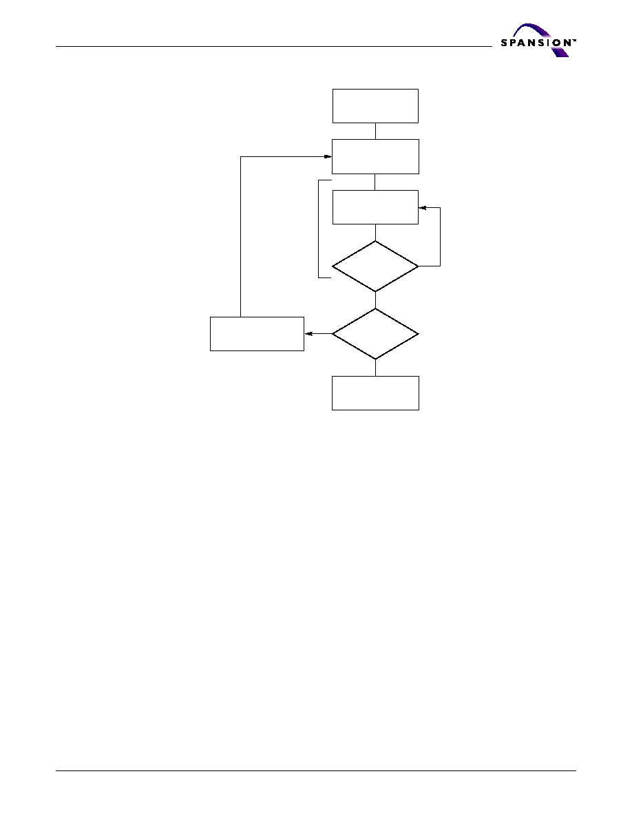
March 26, 2004 S29JL064HA1
S29JL064H
33
P r e l i m i n a r y
Figure 4. Program Operation
Chip Erase Command Sequence
Chip erase is a six bus cycle operation. The chip erase command sequence is ini-
tiated by writing two unlock cycles, followed by a set-up command. Two
additional unlock write cycles are then followed by the chip erase command,
which in turn invokes the Embedded Erase algorithm. The device does not require
the system to preprogram prior to erase. The Embedded Erase algorithm auto-
matically preprograms and verifies the entire memory for an all zero data pattern
prior to electrical erase. The system is not required to provide any controls or tim-
ings during these operations. Table
4
shows the address and data requirements
for the chip erase command sequence.
When the Embedded Erase algorithm is complete, that bank returns to the read
mode and addresses are no longer latched. The system can determine the status
of the erase operation by using DQ7, DQ6, DQ2, or RY/BY#. Refer to the Write
Operation Status section for information on these status bits.
Any commands written during the chip erase operation are ignored. However,
note that a hardware reset immediately terminates the erase operation. If that
occurs, the chip erase command sequence should be reinitiated once that bank
has returned to reading array data, to ensure data integrity. Note that the SecSi
Sector, autoselect, and CFI functions are unavailable when an erase operation is
in progress.
START
Write Program
Command Sequence
Data Poll
from System
Verify Data?
No
Yes
Last Address?
No
Yes
Programming
Completed
Increment Address
Embedded
Program
algorithm
in progress
Note: See Table
4
for program command sequence.

34
S29JL064H
S29JL064HA1 March 26, 2004
P r e l i m i n a r y
5 illustrates the algorithm for the erase operation. Refer to the Erase and Program
Operations tables in the AC Characteristics section for parameters, and
Figure 20
section for timing diagrams.
Sector Erase Command Sequence
Sector erase is a six bus cycle operation. The sector erase command sequence is
initiated by writing two unlock cycles, followed by a set-up command. Two addi-
tional unlock cycles are written, and are then followed by the address of the
sector to be erased, and the sector erase command. Table
4
shows the address
and data requirements for the sector erase command sequence.
The device does not require the system to preprogram prior to erase. The Em-
bedded Erase algorithm automatically programs and verifies the entire sector for
an all zero data pattern prior to electrical erase. The system is not required to
provide any controls or timings during these operations.
After the command sequence is written, a sector erase time-out of 80 µs occurs.
During the time-out period, additional sector addresses and sector erase com-
mands may be written. Loading the sector erase buffer may be done in any
sequence, and the number of sectors may be from one sector to all sectors. The
time between these additional cycles must be less than 80 µs, otherwise erasure
may begin. Any sector erase address and command following the exceeded time-
out may or may not be accepted. It is recommended that processor interrupts be
disabled during this time to ensure all commands are accepted. The interrupts
can be re-enabled after the last Sector Erase command is written. Any com-
mand other than Sector Erase or Erase Suspend during the time-out
period resets that bank to the read mode. The system must rewrite the com-
mand sequence and any additional addresses and commands.
The system can monitor DQ3 to determine if the sector erase timer has timed out
(See the section on DQ3: Sector Erase Timer.). The time-out begins from the ris-
ing edge of the final WE# or CE# pulse (first rising edge) in the command
sequence.
When the Embedded Erase algorithm is complete, the bank returns to reading
array data and addresses are no longer latched. Note that while the Embedded
Erase operation is in progress, the system can read data from the non-erasing
bank. The system can determine the status of the erase operation by reading
DQ7, DQ6, DQ2, or RY/BY# in the erasing bank. Refer to the Write Operation Sta-
tus section for information on these status bits.
Once the sector erase operation has begun, only the Erase Suspend command is
valid. All other commands are ignored. However, note that a hardware reset im-
mediately terminates the erase operation. If that occurs, the sector erase
command sequence should be reinitiated once that bank has returned to reading
array data, to ensure data integrity. Note that the SecSi Sector, autoselect, and
CFI functions are unavailable when an erase operation is in progress.
5 illustrates the algorithm for the erase operation. Refer to the Erase and Program
Operations tables in the AC Characteristics section for parameters, and
Figure 20
section for timing diagrams.
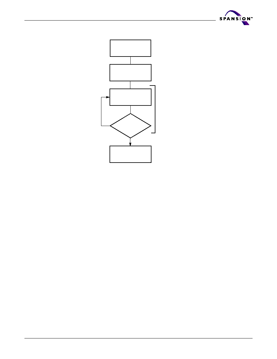
March 26, 2004 S29JL064HA1
S29JL064H
35
P r e l i m i n a r y
Figure 5. Erase Operation
Erase Suspend/Erase Resume Commands
The Erase Suspend command, B0h, allows the system to interrupt a sector erase
operation and then read data from, or program data to, any sector not selected
for erasure. The bank address is required when writing this command. This com-
mand is valid only during the sector erase operation, including the 80 µs time-out
period during the sector erase command sequence. The Erase Suspend command
is ignored if written during the chip erase operation or Embedded Program
algorithm. The bank address must contain one of the sectors currently selected
for erase.
When the Erase Suspend command is written during the sector erase operation,
the device requires a maximum of 20 µs to suspend the erase operation. How-
ever, when the Erase Suspend command is written during the sector erase
time-out, the device immediately terminates the time-out period and suspends
the erase operation.
After the erase operation has been suspended, the bank enters the erase-sus-
pend-read mode. The system can read data from or program data to any sector
not selected for erasure. (The device "erase suspends" all sectors selected for
erasure.) Reading at any address within erase-suspended sectors produces sta-
tus information on DQ7≠DQ0. The system can use DQ7, or DQ6 and DQ2
together, to determine if a sector is actively erasing or is erase-suspended. Refer
to the Write Operation Status section for information on these status bits.
START
Write Erase
Command Sequence
(Notes 1, 2)
Data Poll to Erasing
Bank from System
Data = FFh?
No
Yes
Erasure Completed
Embedded
Erase
algorithm
in progress
Notes:
1. See Table
4
for erase command sequence.
2. See the section on DQ3 for information on the sector
erase timer.

36
S29JL064H
S29JL064HA1 March 26, 2004
P r e l i m i n a r y
After an erase-suspended program operation is complete, the bank returns to the
erase-suspend-read mode. The system can determine the status of the program
operation using the DQ7 or DQ6 status bits, just as in the standard Byte Program
operation. Refer to the Write Operation Status section for more information.
In the erase-suspend-read mode, the system can also issue the autoselect com-
mand sequence. The device allows reading autoselect codes even at addresses
within erasing sectors, since the codes are not stored in the memory array. When
the device exits the autoselect mode, the device reverts to the Erase Suspend
mode, and is ready for another valid operation. Refer to the Autoselect Mode and
Autoselect Command Sequence sections for details.
To resume the sector erase operation, the system must write the Erase Resume
command. The bank address of the erase-suspended bank is required when writ-
ing this command. Further writes of the Resume command are ignored. Another
Erase Suspend command can be written after the chip has resumed erasing.
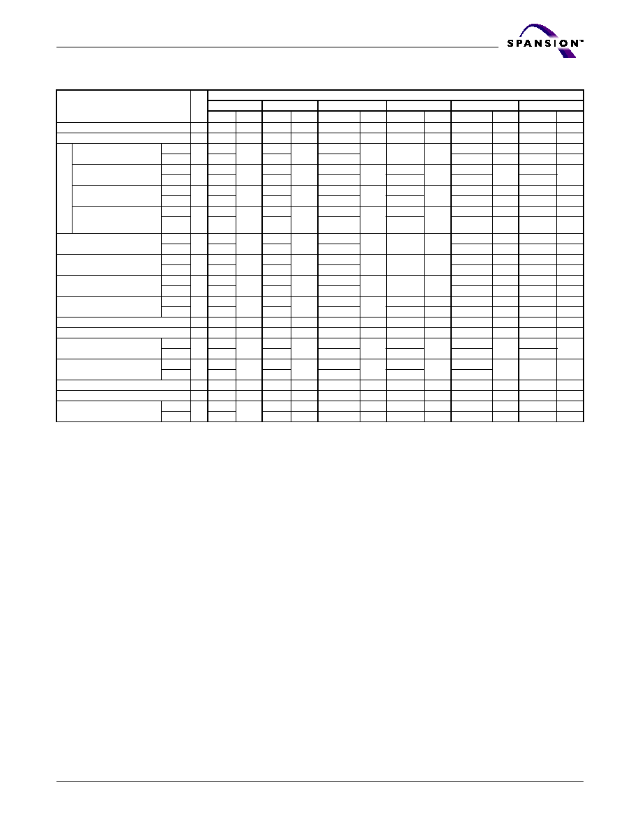
March 26, 2004 S29JL064HA1
S29JL064H
37
P r e l i m i n a r y
Table 4. S29JL064H Command Definitions
Command
Sequence
(Note 1)
Cycle
s
Bus Cycles (Notes 2≠5)
First
Second
Third
Fourth
Fifth
Sixth
Addr Data Addr Data
Addr
Data
Addr
Data
Addr
Data
Addr
Data
Read (Note 6)
1
RA
RD
Reset (Note 7)
1
XXX
F0
Auto
s
e
lec
t
(N
ot
e
8
)
Manufacturer ID
Word
4
555
AA
2AA
55
(BA)555
90
(BA)X00
01
Byte
AAA
555
(BA)AAA
Device ID (Note 9)
Word
6
555
AA
2AA
55
(BA)555
90
(BA)X01
7E
(BA)X0E
02
(BA)X0F
01
Byte
AAA
555
(BA)AAA
(BA)X02
(BA)X1C
(BA)X1E
SecSi Sector Factory
Protect (Note 10)
Word
4
555
AA
2AA
55
(BA)555
90
(BA)X03
80/
00
Byte
AAA
555
(BA)AAA
(BA)X06
Sector/Sector Block
Protect Verify
(Note 11)
Word
4
555
AA
2AA
55
(BA)555
90
(SA)X02
00/
01
Byte
AAA
555
(BA)AAA
(SA)X04
Enter SecSi Sector Region
Word
3
555
AA
2AA
55
555
88
Byte
AAA
555
AAA
Exit SecSi Sector Region
Word
4
555
AA
2AA
55
555
90
XXX
00
Byte
AAA
555
AAA
Program
Word
4
555
AA
2AA
55
555
A0
PA
PD
Byte
AAA
555
AAA
Unlock Bypass
Word
3
555
AA
2AA
55
555
20
Byte
AAA
555
AAA
Unlock Bypass Program (Note 12)
2
XXX
A0
PA
PD
Unlock Bypass Reset (Note 13)
2
XXX
90
XXX
00
Chip Erase
Word
6
555
AA
2AA
55
555
80
555
AA
2AA
55
555
10
Byte
AAA
555
AAA
AAA
555
AAA
Sector Erase
Word
6
555
AA
2AA
55
555
80
555
AA
2AA
55
SA
30
Byte
AAA
555
AAA
AAA
555
Erase Suspend (Note 14)
1
BA
B0
Erase Resume (Note 15)
1
BA
30
CFI Query (Note )
Word
1
55
98
Byte
AA
Legend:
X = Don't care
RA = Address of the memory location to be read.
RD = Data read from location RA during read operation.
PA = Address of the memory location to be programmed. Addresses
latch on the falling edge of the WE# or CE# pulse, whichever happens
later.
PD = Data to be programmed at location PA. Data latches on the rising
edge of WE# or CE# pulse, whichever happens first.
SA = Address of the sector to be verified (in autoselect mode) or
erased. Address bits A21≠A12 uniquely select any sector. Refer to
Table
3
for information on sector addresses.
BA = Address of the bank that is being switched to autoselect mode, is
in bypass mode, or is being erased. A21≠A19 uniquely select a bank.
Notes:
1. See Table
1
for description of bus operations.
2. All values are in hexadecimal.
3. Except for the read cycle and the fourth, fifth, and sixth cycle of
the autoselect command sequence, all bus cycles are write
cycles.
4. Data bits DQ15≠DQ8 are don't care in command sequences,
except for RD and PD.
5. Unless otherwise noted, address bits A21≠A11 are don't cares for
unlock and command cycles, unless SA or PA is required.
6. No unlock or command cycles required when bank is reading
array data.
7. The Reset command is required to return to the read mode (or to
the erase-suspend-read mode if previously in Erase Suspend)
when a bank is in the autoselect mode, or if DQ5 goes high
(while the bank is providing status information).
8. The fourth cycle of the autoselect command sequence is a read
cycle. The system must provide the bank address to obtain the
manufacturer ID, device ID, or SecSi Sector factory protect
information. Data bits DQ15≠DQ8 are don't care. While reading
the autoselect addresses, the bank address must be the same
until a reset command is given. See the Autoselect Command
Sequence section for more information.
9. The device ID must be read across the fourth, fifth, and sixth
cycles.
10. The data is 80h for factory locked, 40h for customer locked, and
00h for not factory/customer locked.
11. The data is 00h for an unprotected sector/sector block and 01h
for a protected sector/sector block.
12. The Unlock Bypass command is required prior to the Unlock
Bypass Program command.
13. The Unlock Bypass Reset command is required to return to the
read mode when the bank is in the unlock bypass mode.
14. The system may read and program in non-erasing sectors, or
enter the autoselect mode, when in the Erase Suspend mode.
The Erase Suspend command is valid only during a sector erase
operation, and requires the bank address.
15. The Erase Resume command is valid only during the Erase
Suspend mode, and requires the bank address.
Command is valid when device is ready to read array data or when
device is in autoselect mode.

38
S29JL064H
S29JL064HA1 March 26, 2004
P r e l i m i n a r y
Write Operation Status
The device provides several bits to determine the status of a program or erase
operation: DQ2, DQ3, DQ5, DQ6, and DQ7. Table
9
and the following subsections
describe the function of these bits. DQ7 and DQ6 each offer a method for deter-
mining whether a program or erase operation is complete or in progress. The
device also provides a hardware-based output signal, RY/BY#, to determine
whether an Embedded Program or Erase operation is in progress or has been
completed.
DQ7: Data# Polling
The Data# Polling bit, DQ7, indicates to the host system whether an Embedded
Program or Erase algorithm is in progress or completed, or whether a bank is in
Erase Suspend. Data# Polling is valid after the rising edge of the final WE# pulse
in the command sequence.
During the Embedded Program algorithm, the device outputs on DQ7 the com-
plement of the datum programmed to DQ7. This DQ7 status also applies to
programming during Erase Suspend. When the Embedded Program algorithm is
complete, the device outputs the datum programmed to DQ7. The system must
provide the program address to read valid status information on DQ7. If a pro-
gram address falls within a protected sector, Data# Polling on DQ7 is active for
approximately 1 µs, then that bank returns to the read mode.
During the Embedded Erase algorithm, Data# Polling produces a "0" on DQ7.
When the Embedded Erase algorithm is complete, or if the bank enters the Erase
Suspend mode, Data# Polling produces a "1" on DQ7. The system must provide
an address within any of the sectors selected for erasure to read valid status in-
formation on DQ7.
After an erase command sequence is written, if all sectors selected for erasing
are protected, Data# Polling on DQ7 is active for approximately 100 µs, then the
bank returns to the read mode. If not all selected sectors are protected, the Em-
bedded Erase algorithm erases the unprotected sectors, and ignores the selected
sectors that are protected. However, if the system reads DQ7 at an address within
a protected sector, the status may not be valid.
When the system detects DQ7 has changed from the complement to true data,
it can read valid data at DQ15≠DQ0 (or DQ7≠DQ0 for x8-only device) on the fol-
lowing read cycles. Just prior to the completion of an Embedded Program or Erase
operation, DQ7 may change asynchronously with DQ15≠DQ8 (DQ7≠DQ0 for x8-
only device) while Output Enable (OE#) is asserted low. That is, the device may
change from providing status information to valid data on DQ7. Depending on
when the system samples the DQ7 output, it may read the status or valid data.
Even if the device has completed the program or erase operation and DQ7 has
valid data, the data outputs on DQ15≠DQ0 may be still invalid. Valid data on
DQ15≠DQ0 (or DQ7≠DQ0 for x8-only device) will appear on successive read
cycles.
Table
9
shows the outputs for Data# Polling on DQ7. 6 shows the Data# Polling
algorithm. 22 in the AC Characteristics section shows the Data# Polling timing
diagram.
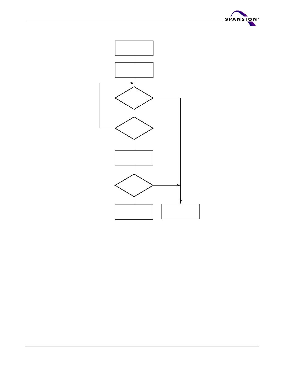
March 26, 2004 S29JL064HA1
S29JL064H
39
P r e l i m i n a r y
Figure 6. Data# Polling Algorithm
DQ7 = Data?
Yes
No
No
DQ5 = 1?
No
Yes
Yes
FAIL
PASS
Read DQ7≠DQ0
Addr = VA
Read DQ7≠DQ0
Addr = VA
DQ7 = Data?
START
Notes:
1. VA = Valid address for programming. During a
sector erase operation, a valid address is any sector
address within the sector being erased. During chip
erase, a valid address is any non-protected sector
address.
2. DQ7 should be rechecked even if DQ5 = "1" because
DQ7 may change simultaneously with DQ5.

40
S29JL064H
S29JL064HA1 March 26, 2004
P r e l i m i n a r y
RY/BY#: Ready/Busy#
The RY/BY# is a dedicated, open-drain output pin which indicates whether an
Embedded Algorithm is in progress or complete. The RY/BY# status is valid after
the rising edge of the final WE# pulse in the command sequence. Since RY/BY#
is an open-drain output, several RY/BY# pins can be tied together in parallel with
a pull-up resistor to V
CC
.
If the output is low (Busy), the device is actively erasing or programming. (This
includes programming in the Erase Suspend mode.) If the output is high (Ready),
the device is in the read mode, the standby mode, or one of the banks is in the
erase-suspend-read mode.
Table
9
shows the outputs for RY/BY#.
DQ6: Toggle Bit I
Toggle Bit I on DQ6 indicates whether an Embedded Program or Erase algorithm
is in progress or complete, or whether the device has entered the Erase Suspend
mode. Toggle Bit I may be read at any address, and is valid after the rising edge
of the final WE# pulse in the command sequence (prior to the program or erase
operation), and during the sector erase time-out.
During an Embedded Program or Erase algorithm operation, successive read cy-
cles to any address cause DQ6 to toggle. The system may use either OE# or CE#
to control the read cycles. When the operation is complete, DQ6 stops toggling.
After an erase command sequence is written, if all sectors selected for erasing
are protected, DQ6 toggles for approximately 100 µs, then returns to reading
array data. If not all selected sectors are protected, the Embedded Erase algo-
rithm erases the unprotected sectors, and ignores the selected sectors that are
protected.
The system can use DQ6 and DQ2 together to determine whether a sector is ac-
tively erasing or is erase-suspended. When the device is actively erasing (that is,
the Embedded Erase algorithm is in progress), DQ6 toggles. When the device en-
ters the Erase Suspend mode, DQ6 stops toggling. However, the system must
also use DQ2 to determine which sectors are erasing or erase-suspended. Alter-
natively, the system can use DQ7 (see the subsection on DQ7: Data# Polling).
If a program address falls within a protected sector, DQ6 toggles for approxi-
mately 1 µs after the program command sequence is written, then returns to
reading array data.
DQ6 also toggles during the erase-suspend-program mode, and stops toggling
once the Embedded Program algorithm is complete.
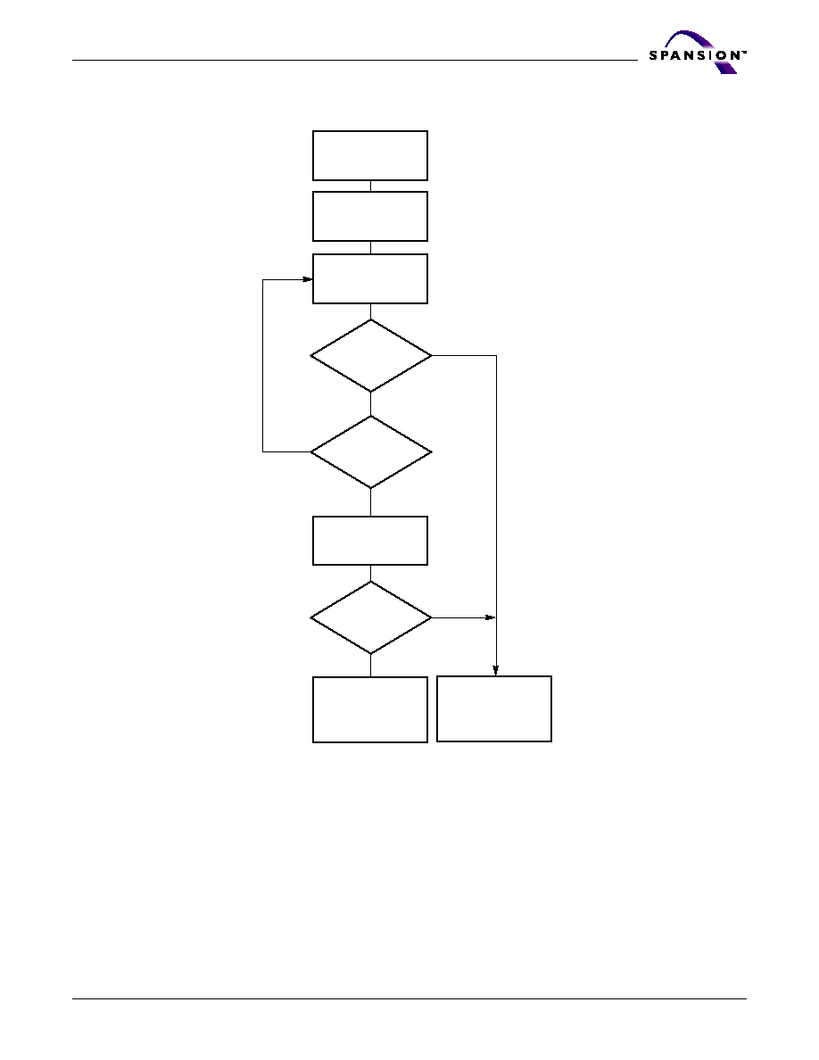
March 26, 2004 S29JL064HA1
S29JL064H
41
P r e l i m i n a r y
Figure 7. Toggle Bit Algorithm
DQ2: Toggle Bit II
The "Toggle Bit II" on DQ2, when used with DQ6, indicates whether a particular
sector is actively erasing (that is, the Embedded Erase algorithm is in progress),
or whether that sector is erase-suspended. Toggle Bit II is valid after the rising
edge of the final WE# pulse in the command sequence.
START
No
Yes
Yes
DQ5 = 1?
No
Yes
Toggle Bit
= Toggle?
No
Program/Erase
Operation Not
Complete, Write
Reset Command
Program/Erase
Operation Complete
Toggle Bit
= Toggle?
Read Byte Twice
(DQ7≠DQ0)
Address = VA
Read Byte
(DQ7≠DQ0)
Address =VA
Read Byte
(DQ7≠DQ0)
Address =VA
Note: The system should recheck the toggle bit even if
DQ5 = "1" because the toggle bit may stop toggling as DQ5
changes to "1." See the subsections on DQ6 and DQ2 for
more information.

42
S29JL064H
S29JL064HA1 March 26, 2004
P r e l i m i n a r y
DQ2 toggles when the system reads at addresses within those sectors that have
been selected for erasure. (The system may use either OE# or CE# to control the
read cycles.) But DQ2 cannot distinguish whether the sector is actively erasing or
is erase-suspended. DQ6, by comparison, indicates whether the device is actively
erasing, or is in Erase Suspend, but cannot distinguish which sectors are selected
for erasure. Thus, both status bits are required for sector and mode information.
Refer to Table
9
to compare outputs for DQ2 and DQ6.
7 shows the toggle bit algorithm in flowchart form, and the section "DQ2: Toggle
Bit II" explains the algorithm. See also the DQ6: Toggle Bit I subsection. 23
shows the toggle bit timing diagram. 24 shows the differences between DQ2 and
DQ6 in graphical form.
Reading Toggle Bits DQ6/DQ2
Refer to 7 for the following discussion. Whenever the system initially begins read-
ing toggle bit status, it must read DQ15≠DQ0 (or DQ7≠DQ0 for x8-only device)
at least twice in a row to determine whether a toggle bit is toggling. Typically, the
system would note and store the value of the toggle bit after the first read. After
the second read, the system would compare the new value of the toggle bit with
the first. If the toggle bit is not toggling, the device has completed the program
or erase operation. The system can read array data on DQ15≠DQ0 (or DQ7≠DQ0
for x8-only device) on the following read cycle.
However, if after the initial two read cycles, the system determines that the toggle
bit is still toggling, the system also should note whether the value of DQ5 is high
(see the section on DQ5). If it is, the system should then determine again
whether the toggle bit is toggling, since the toggle bit may have stopped toggling
just as DQ5 went high. If the toggle bit is no longer toggling, the device has suc-
cessfully completed the program or erase operation. If it is still toggling, the
device did not completed the operation successfully, and the system must write
the reset command to return to reading array data.
The remaining scenario is that the system initially determines that the toggle bit
is toggling and DQ5 has not gone high. The system may continue to monitor the
toggle bit and DQ5 through successive read cycles, determining the status as de-
scribed in the previous paragraph. Alternatively, it may choose to perform other
system tasks. In this case, the system must start at the beginning of the algo-
rithm when it returns to determine the status of the operation (top of 7).
DQ5: Exceeded Timing Limits
DQ5 indicates whether the program or erase time has exceeded a specified in-
ternal pulse count limit. Under these conditions DQ5 produces a "1," indicating
that the program or erase cycle was not successfully completed.
The device may output a "1" on DQ5 if the system tries to program a "1" to a
location that was previously programmed to "0." Only an erase operation can
change a "0" back to a "1." Under this condition, the device halts the opera-
tion, and when the timing limit has been exceeded, DQ5 produces a "1."
Under both these conditions, the system must write the reset command to return
to the read mode (or to the erase-suspend-read mode if a bank was previously
in the erase-suspend-program mode).
DQ3: Sector Erase Timer
After writing a sector erase command sequence, the system may read DQ3 to de-
termine whether or not erasure has begun. (The sector erase timer does not

March 26, 2004 S29JL064HA1
S29JL064H
43
P r e l i m i n a r y
apply to the chip erase command.) If additional sectors are selected for erasure,
the entire time-out also applies after each additional sector erase command.
When the time-out period is complete, DQ3 switches from a "0" to a "1." If the
time between additional sector erase commands from the system can be as-
sumed to be less than 50 µs, the system need not monitor DQ3. See also the
Sector Erase Command Sequence section.
After the sector erase command is written, the system should read the status of
DQ7 (Data# Polling) or DQ6 (Toggle Bit I) to ensure that the device has accepted
the command sequence, and then read DQ3. If DQ3 is "1," the Embedded Erase
algorithm has begun; all further commands (except Erase Suspend) are ignored
until the erase operation is complete. If DQ3 is "0," the device will accept addi-
tional sector erase commands. To ensure the command has been accepted, the
system software should check the status of DQ3 prior to and following each sub-
sequent sector erase command. If DQ3 is high on the second status check, the
last command might not have been accepted.
Table
9
shows the status of DQ3 relative to the other status bits.
Table 9. Write Operation Status
Notes:
1. DQ5 switches to `1' when an Embedded Program or Embedded Erase operation has exceeded the maximum timing
limits. Refer to the section on DQ5 for more information.
2. DQ7 and DQ2 require a valid address when reading status information. Refer to the appropriate subsection for further
details.
3. When reading write operation status bits, the system must always provide the bank address where the Embedded
Algorithm is in progress. The device outputs array data if the system addresses a non-busy bank.
Status
DQ7
(Note 2)
DQ6
DQ5
(Note 1)
DQ3
DQ2
(Note 2)
RY/BY#
Standard
Mode
Embedded Program Algorithm
DQ7#
Toggle
0
N/A
No toggle
0
Embedded Erase Algorithm
0
Toggle
0
1
Toggle
0
Erase
Suspend
Mode
Erase-Suspend-
Read
Erase
Suspended Sector
1
No toggle
0
N/A
Toggle
1
Non-Erase
Suspended Sector
Data
Data
Data
Data
Data
1
Erase-Suspend-Program
DQ7#
Toggle
0
N/A
N/A
0
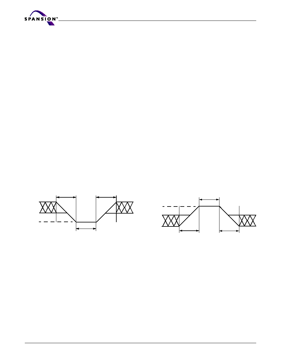
44
S29JL064H
S29JL064HA1 March 26, 2004
P r e l i m i n a r y
Absolute Maximum Ratings
Storage Temperature
Plastic Packages . . . . . . . . . . . . . . . . . . . . . . . . . . . . . . . . . . . . . . .≠65∞C to +150∞C
Ambient Temperature
with Power Applied . . . . . . . . . . . . . . . . . . . . . . . . . . . . . . . . . . . . .≠65∞C to +125∞C
Voltage with Respect to Ground
V
CC
(Note 1). . . . . . . . . . . . . . . . . . . . . . . . . . . . . . . . . . . . . . . . . . ≠0.5 V to +4.0 V
A9, OE#, and RESET#
(Note 2). . . . . . . . . . . . . . . . . . . . . . . . . . . . . . . . . . . . . . . . . . . . ≠0.5 V to +12.5 V
WP#/ACC. . . . . . . . . . . . . . . . . . . . . . . . . . . . . . . . . . . . . . . . . . . ≠0.5 V to +10.5 V
All other pins (Note 1) . . . . . . . . . . . . . . . . . . . . . . . . . . . . . . . . ≠0.5 V to V
CC
+0.5 V
Output Short Circuit Current (Note 3) . . . . . . . . . . . . . . . . . . . . . . . . . . . . . . 200 mA
Notes:
1. Minimum DC voltage on input or I/O pins is ≠0.5 V. During voltage transitions, input or I/O pins may overshoot V
SS
to ≠
2.0 V for periods of up to 20 ns. Maximum DC voltage on input or I/O pins is V
CC
+0.5 V. See
Figure 8
. During voltage
transitions, input or I/O pins may overshoot to V
CC
+2.0 V for periods up to 20 ns. See
Figure 9
.
2. Minimum DC input voltage on pins A9, OE#, RESET#, and WP#/ACC is ≠0.5 V. During voltage transitions, A9, OE#, WP#/
ACC, and RESET# may overshoot V
SS
to ≠2.0 V for periods of up to 20 ns. See
Figure 8
. Maximum DC input voltage on
pin A9 is +12.5 V which may overshoot to +14.0 V for periods up to 20 ns. Maximum DC input voltage on WP#/ACC is
+9.5 V which may overshoot to +12.0 V for periods up to 20 ns.
3. No more than one output may be shorted to ground at a time. Duration of the short circuit should not be greater than one
second.
Stresses above those listed under "Absolute Maximum Ratings" may cause permanent damage to the device. This is a stress
rating only; functional operation of the device at these or any other conditions above those indicated in the operational
sections of this data sheet is not implied. Exposure of the device to absolute maximum rating conditions for extended periods
may affect device reliability.
Operating Ranges
Industrial (I) Devices
Ambient Temperature (T
A
) . . . . . . . . . . . . . . . . . . . . . . . . . ≠40∞C to +85∞C
Extended (N) Devices
Ambient Temperature (T
A
) . . . . . . . . . . . . . . . . . . . . . . . . ≠55∞C to +125∞C
V
CC
Supply Voltages
V
CC
for standard voltage range . . . . . . . . . . . . . . . . . . . . . . . .2.7 V to 3.6 V
Operating ranges define those limits between which the functionality of the device is
guaranteed.
Figure 8. Maximum Negative
Overshoot Waveform
Figure 9. Maximum Positive
Overshoot Waveform
20 ns
20 ns
+0.8 V
≠0.5 V
20 ns
≠2.0 V
20 ns
20 ns
V
CC
+2.0 V
V
CC
+0.5 V
20 ns
2.0 V
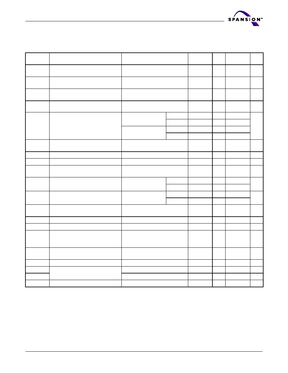
March 26, 2004 S29JL064HA1
S29JL064H
45
P r e l i m i n a r y
DC Characteristics
CMOS Compatible
Notes:
1. The I
CC
current listed is typically less than 2 mA/MHz, with OE# at V
IH
.
2. Maximum I
CC
specifications are tested with V
CC
= V
CC
max.
3. I
CC
active while Embedded Erase or Embedded Program is in progress.
4. Automatic sleep mode enables the low power mode when addresses remain stable for t
ACC
+ 30 ns. Typical sleep mode
current is 200 nA.
5. Not 100% tested.
Paramete
r Symbol
Parameter Description
Test Conditions
Min
Typ
Max
Unit
I
LI
Input Load Current
V
IN
= V
SS
to V
CC
,
V
CC
= V
CC
max
±1.0
µA
I
LIT
A9, OE# and RESET# Input Load
Current
V
CC
= V
CC max
, OE# = V
IH
; A9 or
OE# or RESET# = 12.5 V
35
µA
I
LO
Output Leakage Current
V
OUT
= V
SS
to V
CC
,
V
CC
= V
CC max
, OE# = V
IH
±1.0
µA
I
LR
Reset Leakage Current
V
CC
= V
CC max
; RESET# =
12.5 V
35
µA
I
CC1
V
CC
Active Read Current
(Notes 1, 2)
CE# = V
IL
,
OE#
=
V
IH
,
Byte Mode
5 MHz
10
16
mA
1 MHz
2
4
CE# = V
IL
,
OE# =
V
IH
, Word Mode
5 MHz
10
16
1 MHz
2
4
I
CC2
V
CC
Active Write Current (Notes 2,
3)
CE# = V
IL
,
OE# = V
IH
, WE# = V
IL
15
30
mA
I
CC3
V
CC
Standby Current (Note 2)
CE#, RESET# = V
CC
± 0.3 V
0.2
5
µA
I
CC4
V
CC
Reset Current (Note 2)
RESET# = V
SS
± 0.3 V
0.2
5
µA
I
CC5
Automatic Sleep Mode (Notes 2, 4)
V
IH
= V
CC
± 0.3 V;
V
IL
= V
SS
± 0.3 V
0.2
5
µA
I
CC6
V
CC
Active Read-While-Program
Current (Notes 1, 2)
CE# = V
IL
,
OE# = V
IH
Byte
21
45
mA
Word
21
45
I
CC7
V
CC
Active Read-While-Erase
Current (Notes 1, 2)
CE# = V
IL
, OE# = V
IH
Byte
21
45
mA
Word
21
45
I
CC8
V
CC
Active Program-While-Erase-
Suspended Current (Notes 2, 5)
CE# = V
IL
, OE# = V
IH
17
35
mA
V
IL
Input Low Voltage
≠0.5
0.8
V
V
IH
Input High Voltage
0.7 x V
CC
V
CC
+ 0.3
V
V
HH
Voltage for WP#/ACC Sector
Protect/Unprotect and Program
Acceleration
V
CC
= 3.0 V ± 10%
8.5
9.5
V
V
ID
Voltage for Autoselect and
Temporary Sector Unprotect
V
CC
= 3.0 V ± 10%
11.5
12.5
V
V
OL
Output Low Voltage
I
OL
= 2.0 mA, V
CC
= V
CC min
0.45
V
V
OH1
Output High Voltage
I
OH
= ≠2.0 mA, V
CC
= V
CC min
0.85 V
CC
V
V
OH2
I
OH
= ≠100 µA, V
CC
= V
CC min
V
CC
≠0.4
V
LKO
Low V
CC
Lock-Out Voltage (Note 5)
2.3
2.5
V

46
S29JL064H
S29JL064HA1 March 26, 2004
P r e l i m i n a r y
DC Characteristics
Zero-Power Flash
Note: Addresses are switching at 1 MHz
Figure 10. I
CC1
Current vs. Time (Showing Active and Automatic Sleep Currents)
25
20
15
10
5
0
0
500
1000
1500
2000
2500
3000
3500
4000
S
u
p
p
ly
Cu
rr
e
n
t in m
A
Time in ns
10
8
2
0
1
2
3
4
5
Frequency in MHz
S
upply
C
u
rr
e
n
t in
mA
Note: T = 25 ∞C
Figure 11. Typical I
CC1
vs. Frequency
2.7 V
3.6 V
4
6
12
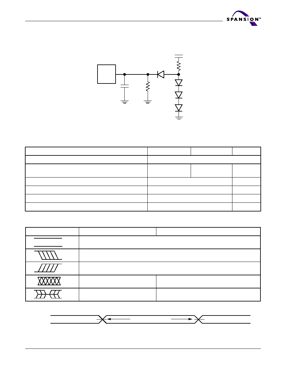
March 26, 2004 S29JL064HA1
S29JL064H
47
P r e l i m i n a r y
Test Conditions
Table 5. Test Specifications
Key To Switching Waveforms
Test Condition
55, 60
70, 90
Unit
Output Load
1 TTL gate
Output Load Capacitance, C
L
(including jig capacitance)
30
100
pF
Input Rise and Fall Times
5
ns
Input Pulse Levels
0.0≠3.0
V
Input timing measurement reference levels
1.5
V
Output timing measurement reference levels
1.5
V
2.7 k
CL
6.2 k
3.3 V
Device
Under
Test
Note: Diodes are IN3064 or equivalent
Figure 12. Test Setup
WAVEFORM
INPUTS
OUTPUTS
Steady
Changing from H to L
Changing from L to H
Don't Care, Any Change Permitted
Changing, State Unknown
Does Not Apply
Center Line is High Impedance State (High Z)
3.0 V
0.0 V
1.5 V
1.5 V
Output
Measurement Level
Input
Figure 13. Input Waveforms and Measurement Levels
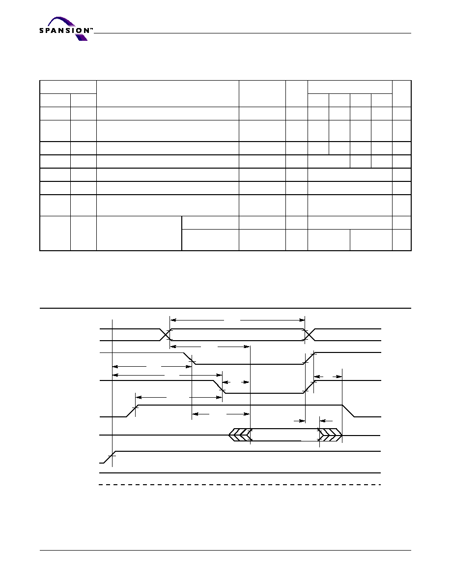
48
S29JL064H
S29JL064HA1 March 26, 2004
P r e l i m i n a r y
AC Characteristics
Read-Only Operations
Notes:
1. Not 100% tested.
2. See 12 and Table
5
for test specifications
3. Measurements performed by placing a 50 ohm termination on the data pin with a bias of V
CC
/2. The time from OE#
high to the data bus driven to V
CC
/2 is taken as t
DF
.
Parameter
Description
Test Setup
Speed Options
JEDEC
Std.
55
60
70
90
Unit
t
AVAV
t
RC
Read Cycle Time (Note 1)
Min
55
60
70
90
ns
t
AVQV
t
ACC
Address to Output Delay
CE#,
OE# = V
IL
Max
55
60
70
90
ns
t
ELQV
t
CE
Chip Enable to Output Delay
OE# = V
IL
Max
55
60
70
90
ns
t
GLQV
t
OE
Output Enable to Output Delay
Max
25
30
35
ns
t
EHQZ
t
DF
Chip Enable to Output High Z (Notes 1, 3)
Max
16
ns
t
GHQZ
t
DF
Output Enable to Output High Z (Notes 1, 3)
Max
16
ns
t
AXQX
t
OH
Output Hold Time From Addresses, CE# or
OE#, Whichever Occurs First
Min
0
ns
t
OEH
Output Enable Hold Time
(Note 1)
Read
Min
0
ns
Toggle and
Data# Polling
Min
5
10
ns
t
OH
t
CE
Outputs
WE#
Addresses
CE#
OE#
HIGH Z
Output Valid
HIGH Z
Addresses Stable
t
RC
t
ACC
t
OEH
t
RH
t
OE
t
RH
0 V
RY/BY#
RESET#
t
DF
Figure 14. Read Operation Timings

March 26, 2004 S29JL064HA1
S29JL064H
49
P r e l i m i n a r y
AC Characteristics
Hardware Reset (RESET#)
Note: Not 100% tested.
Parameter
Description
All Speed Options
Unit
JEDEC
Std
t
Ready
RESET# Pin Low (During Embedded Algorithms)
to Read Mode (See Note)
Max
20
µs
t
Ready
RESET# Pin Low (NOT During Embedded
Algorithms) to Read Mode (See Note)
Max
500
ns
t
RP
RESET# Pulse Width
Min
500
ns
t
RH
Reset High Time Before Read (See Note)
Min
50
ns
t
RPD
RESET# Low to Standby Mode
Min
20
µs
t
RB
RY/BY# Recovery Time
Min
0
ns
RESET#
RY/BY#
RY/BY#
t
RP
t
Ready
Reset Timings NOT during Embedded Algorithms
t
Ready
CE#, OE#
t
RH
CE#, OE#
Reset Timings during Embedded Algorithms
RESET#
t
RP
t
RB
Figure 15. Reset Timings
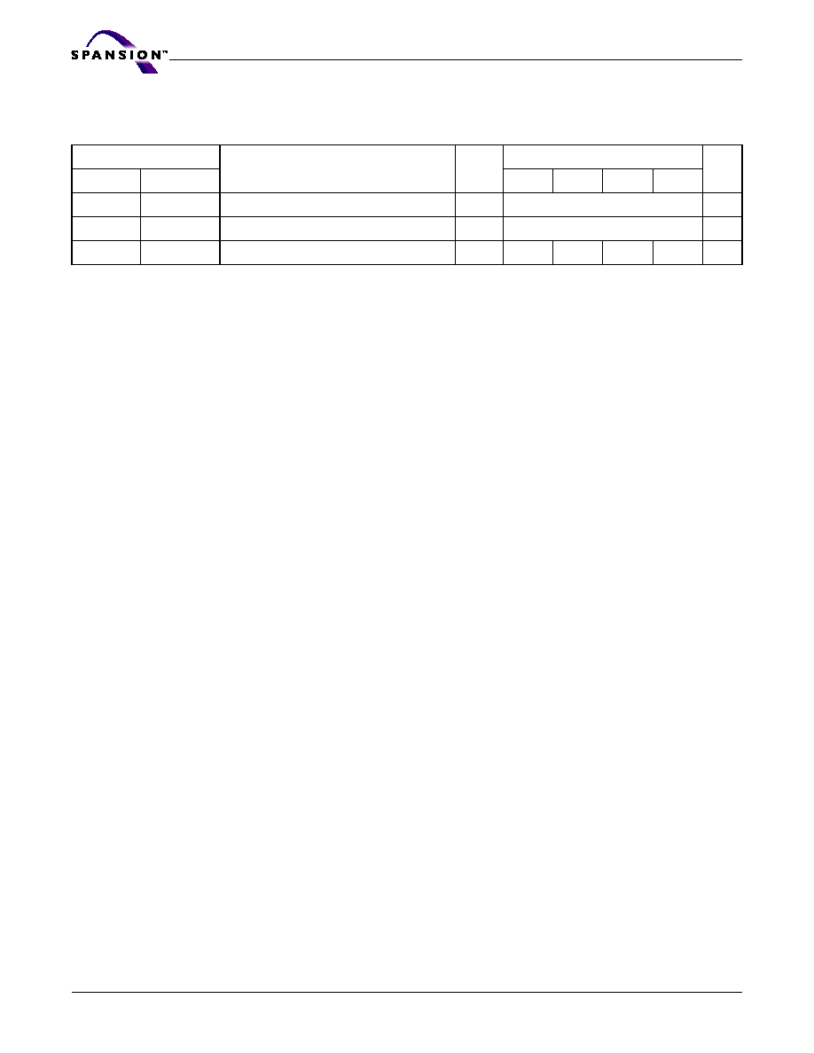
50
S29JL064H
S29JL064HA1 March 26, 2004
P r e l i m i n a r y
AC Characteristics
Word/Byte Configuration (BYTE#)
Parameter
Speed Options
JEDEC
Std.
Description
55
60
70
90
Unit
t
ELFL/
t
ELFH
CE# to BYTE# Switching Low or High
Max
5
ns
t
FLQZ
BYTE# Switching Low to Output HIGH Z
Max
16
ns
t
FHQV
BYTE# Switching High to Output Active
Min
55
60
70
90
ns

March 26, 2004 S29JL064HA1
S29JL064H
51
P r e l i m i n a r y
DQ15
Output
Data Output
(DQ7≠DQ0)
CE#
OE#
BYTE#
t
ELFL
DQ14≠DQ0
Data Output
(DQ14≠DQ0)
DQ15/A-1
Address
Input
t
FLQZ
BYTE#
Switching
from word
to byte
mode
DQ15
Output
Data Output
(DQ7≠DQ0)
BYTE#
t
ELFH
DQ14≠DQ0
Data Output
(DQ14≠DQ0)
DQ15/A-1
Address
Input
t
FHQV
BYTE#
Switching
from byte
to word
mode
Figure 16. BYTE# Timings for Read Operations
Note: Refer to the Erase/Program Operations table for t
AS
and t
AH
specifications.
Figure 17. BYTE# Timings for Write Operations
CE#
WE#
BYTE#
The falling edge of the last WE# signal
t
HOLD
(t
AH
)
t
SET
(t
AS
)

52
S29JL064H
S29JL064HA1 March 26, 2004
P r e l i m i n a r y
AC Characteristics
Erase and Program Operations
Notes:
1. Not 100% tested.
2. See the "Erase And Programming Performance" section for more information.
Parameter
Speed Options
JEDEC
Std
Description
55
60
70
90
Uni
t
t
AVAV
t
WC
Write Cycle Time (Note 1)
Min
55
60
70
90
ns
t
AVWL
t
AS
Address Setup Time
Min
0
ns
t
ASO
Address Setup Time to OE# low during toggle bit
polling
Min
15
ns
t
WLAX
t
AH
Address Hold Time
Min
30
35
40
45
ns
t
AHT
Address Hold Time From CE# or OE# high
during toggle bit polling
Min
0
ns
t
DVWH
t
DS
Data Setup Time
Min
30
35
40
45
ns
t
WHDX
t
DH
Data Hold Time
Min
0
ns
t
OEPH
Output Enable High during toggle bit polling
Min
20
ns
t
GHWL
t
GHWL
Read Recovery Time Before Write
(OE# High to WE# Low)
Min
0
ns
t
ELWL
t
CS
CE# Setup Time
Min
0
ns
t
WHEH
t
CH
CE# Hold Time
Min
0
ns
t
WLWH
t
WP
Write Pulse Width
Min
25
25
30
35
ns
t
WHDL
t
WPH
Write Pulse Width High
Min
25
25
30
30
ns
t
SR/W
Latency Between Read and Write Operations
Min
0
ns
t
WHWH1
t
WHWH1
Programming Operation (Note 2)
Byte
Typ
5
µs
Word
Typ
7
t
WHWH1
t
WHWH1
Accelerated Programming Operation,
Word or Byte (Note 2)
Typ
4
µs
t
WHWH2
t
WHWH2
Sector Erase Operation (Note 2)
Typ
0.4
sec
t
VCS
V
CC
Setup Time (Note 1)
Min
50
µs
t
RB
Write Recovery Time from RY/BY#
Min
0
ns
t
BUSY
Program/Erase Valid to RY/BY# Delay
Max
90
ns
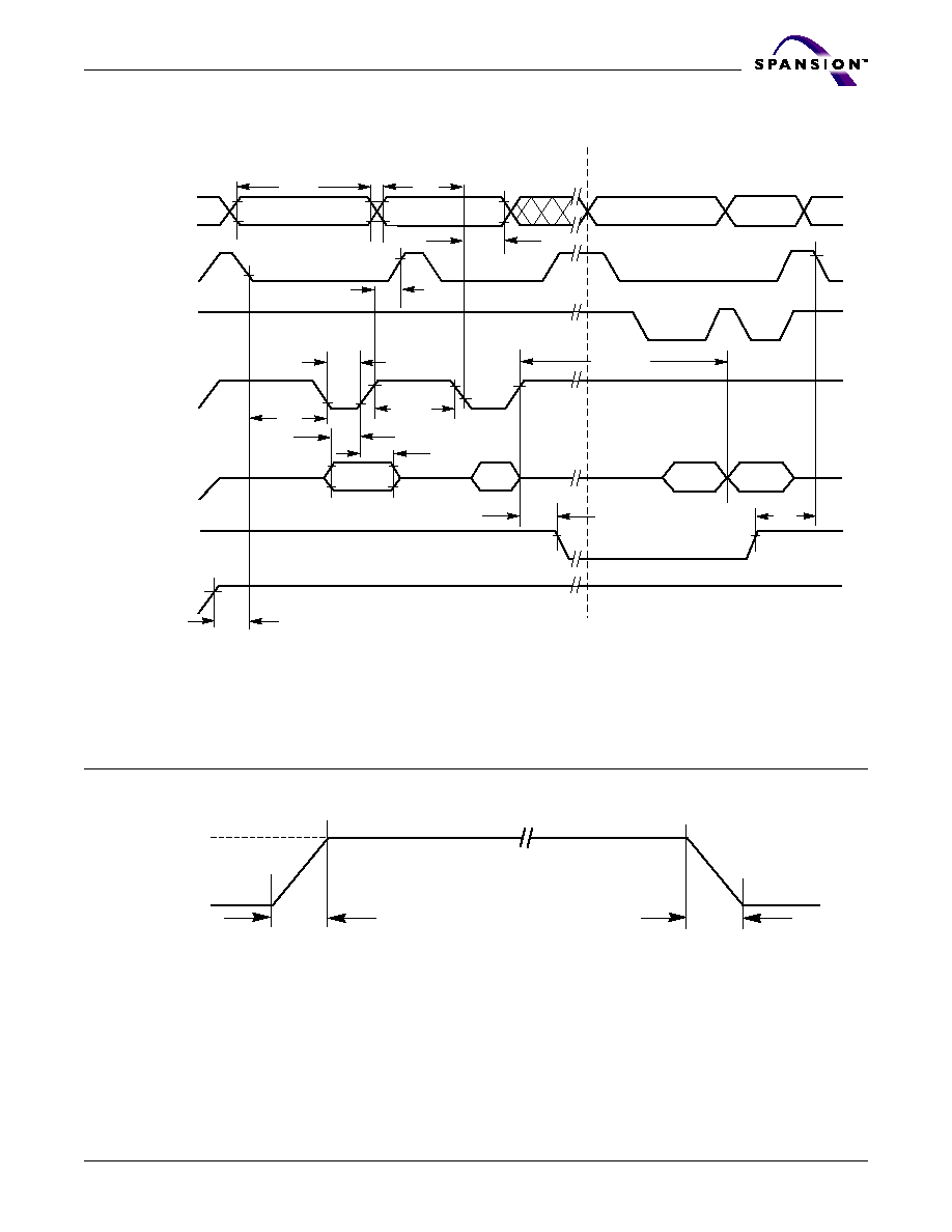
March 26, 2004 S29JL064HA1
S29JL064H
53
P r e l i m i n a r y
AC Characteristics
OE#
WE#
CE#
V
CC
Data
Addresses
t
DS
t
AH
t
DH
t
WP
PD
t
WHWH1
t
WC
t
AS
t
WPH
t
VCS
555h
PA
PA
Read Status Data (last two cycles)
A0h
t
CS
Status
D
OUT
Program Command Sequence (last two cycles)
RY/BY#
t
RB
t
BUSY
t
CH
PA
Notes:
1. PA = program address, PD = program data, D
OUT
is the true data at the program address.
2. Illustration shows device in word mode.
Figure 18. Program Operation Timings
WP#/ACC
t
VHH
V
HH
V
IL
or V
IH
V
IL
or V
IH
t
VHH
Figure 19. Accelerated Program Timing Diagram
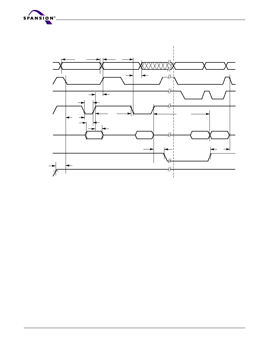
54
S29JL064H
S29JL064HA1 March 26, 2004
P r e l i m i n a r y
AC Characteristics
OE#
CE#
Addresses
V
CC
WE#
Data
2AAh
SA
t
AH
t
WP
t
WC
t
AS
t
WPH
555h for chip erase
10 for Chip Erase
30h
t
DS
t
VCS
t
CS
t
DH
55h
t
CH
In
Progress
Complete
t
WHWH2
VA
VA
Erase Command Sequence (last two cycles)
Read Status Data
RY/BY#
t
RB
t
BUSY
Notes:
1. SA = sector address (for Sector Erase), VA = Valid Address for reading status data (see "Write Operation Status".
2. These waveforms are for the word mode.
Figure 20. Chip/Sector Erase Operation Timings
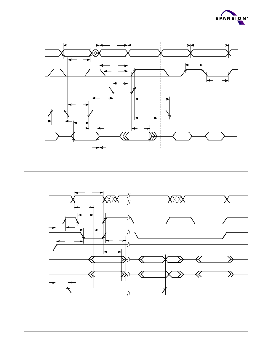
March 26, 2004 S29JL064HA1
S29JL064H
55
P r e l i m i n a r y
AC Characteristics
OE#
CE#
WE#
Addresses
t
OH
Data
Valid
In
Valid
In
Valid PA
Valid RA
t
WC
t
WPH
t
AH
t
WP
t
DS
t
DH
t
RC
t
CE
Valid
Out
t
OE
t
ACC
t
OEH
t
GHWL
t
DF
Valid
In
CE# or CE2# Controlled Write Cycles
WE# Controlled Write Cycle
Valid PA
Valid PA
t
CP
t
CPH
t
WC
t
WC
Read Cycle
t
SR/W
Figure 21. Back-to-back Read/Write Cycle Timings
WE#
CE#
OE#
High Z
t
OE
High Z
DQ7
DQ0≠DQ6
RY/BY#
t
BUSY
Complement
True
Addresses
VA
t
OEH
t
CE
t
CH
t
OH
t
DF
VA
VA
Status Data
Complement
Status Data
True
Valid Data
Valid Data
t
ACC
t
RC
Note: VA = Valid address. Illustration shows first status cycle after command sequence, last status read cycle, and array
data read cycle.
Figure 22. Data# Polling Timings (During Embedded Algorithms)
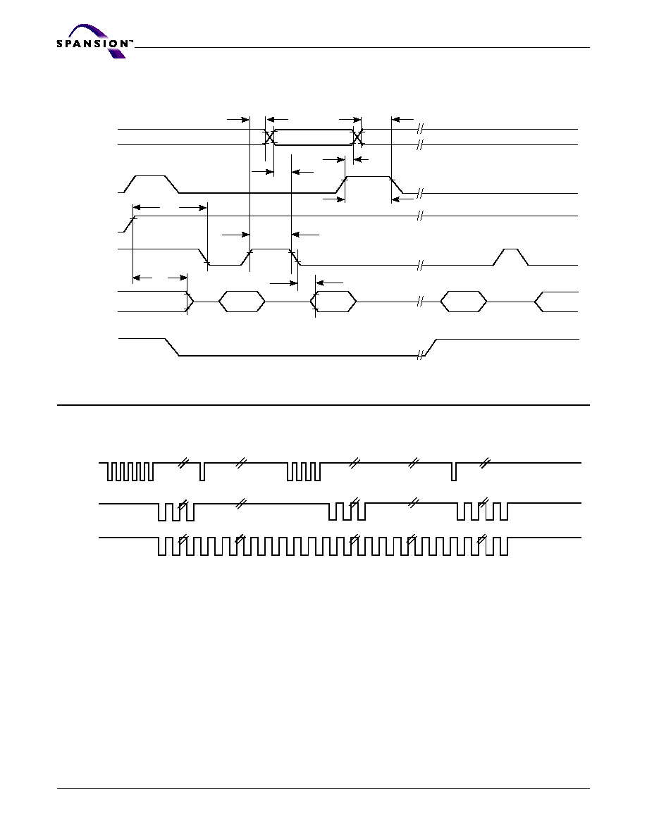
56
S29JL064H
S29JL064HA1 March 26, 2004
P r e l i m i n a r y
AC Characteristics
OE#
CE#
WE#
Addresses
t
OEH
t
DH
t
AHT
t
ASO
t
OEPH
t
OE
Valid Data
(first read)
(second read)
(stops toggling)
t
CEPH
t
AHT
t
AS
DQ6/DQ2
Valid Data
Valid
Status
Valid
Status
Valid
Status
RY/BY#
Note: VA = Valid address; not required for DQ6. Illustration shows first two status cycle after command sequence, last status
read cycle, and array data read cycle
Figure 23. Toggle Bit Timings (During Embedded Algorithms)
Note: DQ2 toggles only when read at an address within an erase-suspended sector. The system may use OE# or CE#
to toggle DQ2 and DQ6.
Figure 24. DQ2 vs. DQ6
Enter
Erase
Erase
Erase
Enter Erase
Suspend Program
Erase Suspend
Read
Erase Suspend
Read
Erase
WE#
DQ6
DQ2
Erase
Complete
Erase
Suspend
Suspend
Program
Resume
Embedded
Erasing

March 26, 2004 S29JL064HA1
S29JL064H
57
P r e l i m i n a r y
AC Characteristics
Temporary Sector Unprotect
Note: Not 100% tested.
Parameter
All Speed Options
JEDEC
Std
Description
Unit
t
VIDR
V
ID
Rise and Fall Time (See Note)
Min
500
ns
t
VHH
V
HH
Rise and Fall Time (See Note)
Min
250
ns
t
RSP
RESET# Setup Time for Temporary Sector
Unprotect
Min
4
µs
t
RRB
RESET# Hold Time from RY/BY# High for
Temporary Sector Unprotect
Min
4
µs
RESET#
t
VIDR
V
ID
V
SS
, V
IL
,
or V
IH
V
ID
V
SS
, V
IL
,
or V
IH
CE#
WE#
RY/BY#
t
VIDR
t
RSP
Program or Erase Command Sequence
t
RRB
Figure 25. Temporary Sector Unprotect Timing Diagram

58
S29JL064H
S29JL064HA1 March 26, 2004
P r e l i m i n a r y
AC Characteristics
Sector Group Protect: 150 µs
Sector Group Unprotect: 15 ms
1 µs
RESET#
SA, A6,
A1, A0
Data
CE#
WE#
OE#
60h
60h
40h
Valid*
Valid*
Valid*
Status
Sector Group Protect/Unprotect
Verify
V
ID
V
IH
* For sector protect, A6 = 0, A1 = 1, A0 = 0. For sector unprotect, A6 = 1, A1 = 1, A0 = 0.
Figure 26. Sector/Sector Block Protect and
Unprotect Timing Diagram
March 26, 2004 S29JL064HA1
S29JL064H
59
P r e l i m i n a r y
AC Characteristics
Alternate CE# Controlled Erase and Program Operations
Notes:
1. Not 100% tested.
2. See the "Erase And Programming Performance" section for more information.
Parameter
Speed Options
JEDEC
Std.
Description
55
60
70
90
Unit
t
AVAV
t
WC
Write Cycle Time (Note 1)
Min
55
55
70
90
ns
t
AVWL
t
AS
Address Setup Time
Min
0
ns
t
ELAX
t
AH
Address Hold Time
Min
30
35
40
45
ns
t
DVEH
t
DS
Data Setup Time
Min
30
35
40
45
ns
t
EHDX
t
DH
Data Hold Time
Min
0
ns
t
GHEL
t
GHEL
Read Recovery Time Before Write
(OE# High to WE# Low)
Min
0
ns
t
WLEL
t
WS
WE# Setup Time
Min
0
ns
t
EHWH
t
WH
WE# Hold Time
Min
0
ns
t
ELEH
t
CP
CE# Pulse Width
Min
25
25
40
45
ns
t
EHEL
t
CPH
CE# Pulse Width High
Min
25
25
30
ns
t
WHWH1
t
WHWH1
Programming Operation
(Note 2)
Byte
Typ
5
µs
Word
Typ
7
t
WHWH1
t
WHWH1
Accelerated Programming Operation,
Word or Byte (Note 2)
Typ
4
µs
t
WHWH2
t
WHWH2
Sector Erase Operation (Note 2)
Typ
0.4
sec

60
S29JL064H
S29JL064HA1 March 26, 2004
P r e l i m i n a r y
AC Characteristics
t
GHEL
t
WS
OE#
CE#
WE#
RESET#
t
DS
Data
t
AH
Addresses
t
DH
t
CP
DQ7#
D
OUT
t
WC
t
AS
t
CPH
PA
Data# Polling
A0 for program
55 for erase
t
RH
t
WHWH1 or 2
RY/BY#
t
WH
PD for program
30 for sector erase
10 for chip erase
555 for program
2AA for erase
PA for program
SA for sector erase
555 for chip erase
t
BUSY
Notes:
1. Figure indicates last two bus cycles of a program or erase operation.
2. PA = program address, SA = sector address, PD = program data.
3. DQ7# is the complement of the data written to the device. D
OUT
is the data written to the device.
4. Waveforms are for the word mode.
Figure 27. Alternate CE# Controlled Write (Erase/Program) Operation Timings

March 26, 2004 S29JL064HA1
S29JL064H
61
P r e l i m i n a r y
Erase And Programming Performance
Notes:
1. Typical program and erase times assume the following conditions: 25∞C, 3.0 V V
CC
, 100,000 cycles; checkerboard data
pattern.
2. Under worst case conditions of 90∞C, V
CC
= 2.7 V, 1,000,000 cycles.
3. The typical chip programming time is considerably less than the maximum chip programming time listed, since most bytes
program faster than the maximum program times listed.
4. In the pre-programming step of the Embedded Erase algorithm, all bytes are programmed to 00h before erasure.
5. System-level overhead is the time required to execute the two- or four-bus-cycle sequence for the program command. See
Table
4
for further information on command definitions.
6. The device has a minimum cycling endurance of 100,000 cycles per sector.
7. Contact the local sales office for minimum cycling endurance values in specific applications and operating conditions.
TSOP & BGA Pin Capacitance
Notes:
1. Sampled, not 100% tested.
2. Test conditions T
A
= 25∞C, f = 1.0 MHz.
Parameter
Typ (Note 1)
Max (Note 2)
Unit
Comments
Sector Erase Time
0.4
5
sec
Excludes 00h programming
prior to erasure (Note 4)
Chip Erase Time
56
sec
Byte Program Time
5
150
µs
Excludes system level
overhead (Note 5)
Accelerated Byte/Word Program Time
4
120
µs
Accelerated Chip Programming Time
10
30
sec
Word Program Time
7
210
µs
Chip Program Time
(Note 3)
Byte Mode
42
126
sec
Word Mode
28
84
Parameter Symbol
Parameter Description
Test Setup
Typ
Max
Unit
C
IN
Input Capacitance
V
IN
= 0
TSOP
6
7.5
pF
Fine-pitch BGA
4.2
5.0
pF
C
OUT
Output Capacitance
V
OUT
= 0
TSOP
8.5
12
pF
Fine-pitch BGA
5.4
6.5
pF
C
IN2
Control Pin Capacitance
V
IN
= 0
TSOP
7.5
9
pF
Fine-pitch BGA
3.9
4.7
pF
62
S29JL064H
S29JL064HA1 March 26, 2004
P r e l i m i n a r y
Physical Dimensions
FBE063--63-Ball Fine-Pitch Ball Grid Array (BGA) 12 x 11 mm package
Dwg rev AF; 10/99
March 26, 2004 S29JL064HA1
S29JL064H
63
P r e l i m i n a r y
Physical Dimensions
TS 048--48-Pin Standard TSOP
Dwg rev AA; 10/99

64
S29JL064H
S29JL064HA1 March 26, 2004
P r e l i m i n a r y
Revision Summary
Revision A (January 22, 2004)
Initial release.
Revision A + 1 (March 26, 2004)
Removed "Latchup Characteristics" section.
Trademarks and Notice
The contents of this document are subject to change without notice.This document may contain information on a Spansion product under development by
FASL LLC. FASL LLC reserves the right to change or discontinue work on any product without notice. The information in this document is provided "as
is" without warranty or guarantee of any kind as to its accuracy, completeness, operability, fitness for particular purpose, merchantability, non-infringement
of third-party rights, or any other warranty, express, implied, or statutory. FASL LLC assumes no liability for any damages of any kind arising out of the use
of the information in this document.
Copyright © 2004 FASL LLC. All rights reserved. Spansion, the Spansion logo,MirrorBit, combinations thereof, and ExpressFlash are trademarks of FASL LLC.
Other company and product names used in this publication are for identification purposes only and may be trademarks of their respective companies.