Document Outline
- General Description
- Product Selector Guide
- Connection Diagram (S71GL032A)
- Pin Description
- Logic Symbol
- Ordering Information
- Physical Dimensions
- General Description
- Product Selector Guide
- Block Diagram
- Pin Descriptions
- Device Bus Operations
- Common Flash Memory Interface (CFI)
- Command Definitions
- Sector Erase Command Sequence
- DC Characteristics
- Test Conditions
- Key to Switching Waveforms
- AC Characteristics
- Erase And Programming Performance
- Type 4 pSRAM
- Type 1 SRAM
- Common Features
- Pin Description
- Functional Description
- Functional Description
- DC Characteristics
- AC Operating Conditions
- AC Characteristics
- Read/Write Characteristics (VCC=2.7-3.3V)
- Data Retention Characteristics (4M Version F)
- Data Retention Characteristics (4M Version G)
- Data Retention Characteristics (8M Version C)
- Data Retention Characteristics (8M Version D)
- Timing Diagrams
- Figure 33. Timing Waveform of Read Cycle(1) (Address Controlled, CS#1=OE#=VIL, CS2=WE#=VIH, UB# and/or LB#=VIL)
- Figure 34. Timing Waveform of Read Cycle(2) (WE#=VIH, if BYTE# is Low, Ignore UB#/LB# Timing)
- Figure 35. Timing Waveform of Write Cycle(1) (WE# controlled, if BYTE# is Low, Ignore UB#/LB# Timing)
- Figure 36. Timing Waveform of Write Cycle(2) (CS# controlled, if BYTE# is Low, Ignore UB#/LB# Timing)
- Figure 37. Timing Waveform of Write Cycle(3) (UB#, LB# controlled)
- Figure 38. Data Retention Waveform
- Revision Summary

Publication Number S71GL032A_00 Revision A Amendment 0 Issue Date March 31, 2005
S71GL032A Based MCPs
Stacked Multi-Chip Product (MCP) Flash Memory and
RAM
32 Megabit (2 M x 16-bit) CMOS 3.0 Volt-only
Page Mode Flash Memory and
16/8/4 Megabit (1M/512K/256K x 16-bit)
Pseudo Static RAM
Data Sheet
ADVANCE
INFORMATION
Notice to Readers: The Advance Information status indicates that this
document contains information on one or more products under development
at Spansion LLC. The information is intended to help you evaluate this product.
Do not design in this product without contacting the factory. Spansion LLC
reserves the right to change or discontinue work on this proposed product
without notice.

Notice On Data Sheet Designations
Spansion LLC issues data sheets with Advance Information or Preliminary designations to advise
readers of product information or intended specifications throughout the product life cycle, including
development, qualification, initial production, and full production. In all cases, however, readers are
encouraged to verify that they have the latest information before finalizing their design. The follow-
ing descriptions of Spansion data sheet designations are presented here to highlight their presence
and definitions.
Advance Information
The Advance Information designation indicates that Spansion LLC is developing one or more specific
products, but has not committed any design to production. Information presented in a document
with this designation is likely to change, and in some cases, development on the product may discon-
tinue. Spansion LLC therefore places the following conditions upon Advance Information content:
"This document contains information on one or more products under development at Spansion LLC. The
information is intended to help you evaluate this product. Do not design in this product without con-
tacting the factory. Spansion LLC reserves the right to change or discontinue work on this proposed
product without notice."
Preliminary
The Preliminary designation indicates that the product development has progressed such that a com-
mitment to production has taken place. This designation covers several aspects of the product life cy-
cle, including product qualification, initial production, and the subsequent phases in the
manufacturing process that occur before full production is achieved. Changes to the technical specifi-
cations presented in a Preliminary document should be expected while keeping these aspects of pro-
duction under consideration. Spansion places the following conditions upon Preliminary content:
"This document states the current technical specifications regarding the Spansion product(s) described
herein. The Preliminary status of this document indicates that product qualification has been completed,
and that initial production has begun. Due to the phases of the manufacturing process that require
maintaining efficiency and quality, this document may be revised by subsequent versions or modifica-
tions due to changes in technical specifications."
Combination
Some data sheets will contain a combination of products with different designations (Advance Infor-
mation, Preliminary, or Full Production). This type of document will distinguish these products and
their designations wherever necessary, typically on the first page, the ordering information page, and
pages with DC Characteristics table and AC Erase and Program table (in the table notes). The dis-
claimer on the first page refers the reader to the notice on this page.
Full Production (No Designation on Document)
When a product has been in production for a period of time such that no changes or only nominal
changes are expected, the Preliminary designation is removed from the data sheet. Nominal changes
may include those affecting the number of ordering part numbers available, such as the addition or
deletion of a speed option, temperature range, package type, or V
IO
range. Changes may also in-
clude those needed to clarify a description or to correct a typographical error or incorrect specifica-
tion. Spansion LLC applies the following conditions to documents in this category:
"This document states the current technical specifications regarding the Spansion product(s) described
herein. Spansion LLC deems the products to have been in sufficient production volume such that sub-
sequent versions of this document are not expected to change. However, typographical or specification
corrections, or modifications to the valid combinations offered may occur."
Questions regarding these document designations may be directed to your local AMD or
Fujitsu sales office.
This document contains information on one or more products under development at Spansion LLC. The information is intended to help you evaluate this product. Do not
design in this product without contacting the factory. Spansion LLC reserves the right to change or discontinue work on this proposed product without notice.
Publication Number S71GL032A_00 Revision A Amendment 0 Issue Date March 31, 2005
General Description
The S71GL series is a product line of stacked Multi-Chip Product (MCP) packages and consists
of:
One S29PL032A (Simultaneous Read/Write) Flash memory die
pSRAM or SRAM
The products covered by this document are listed in the table below:
Distinctive Characteristics
MCP Features
Power supply voltage of 2.7 V to 3.1 V
High performance
-- 100 ns (100 ns Flash, 70 ns pSRAM/SRAM)
Packages
-- 7 x 9 x 1.2 mm 56 ball FBGA
Operating Temperature
-- ≠25∞C to +85∞C
-- ≠40∞C to +85∞C
S71GL032A Based MCPs
Stacked Multi-Chip Product (MCP) Flash Memory and RAM
32 Megabit (2 M x 16-bit) CMOS 3.0 Volt-only
Page Mode Flash Memory and
16/8/4 Megabit (1M/512K/256K x 16-bit)
Pseudo Static RAM
ADVANCE
INFORMATION
Flash Memory Density
32Mb
pSRAM
Density
4Mb
S71GL032A40
8Mb
S71GL032A80/S71GL032A08
4
S71GL032A Based MCPs
S71GL032A_00_A0 March 31, 2005
Product Selector Guide
32 Mb Flash Memory
Device-Model#
Flash Access time (ns) (p)SRAM density (p)SRAM Access time (ns) pSRAM type
Package
S71GL032A40-0B
100
4 M pSRAM
70
pSRAM4
TLC056
S71GL032A40-0F
S71GL032A08-0B
8 M pSRAM
SRAM1
S71GL032A08-0F

March 31, 2005 S71GL032A_00_A0
S71GL032A Based MCPs
5
A d v a n c e I n f o r m a t i o n
Contents
S71GL032A Based MCPs
Product Selector Guide . . . . . . . . . . . . . . . . . . . . . .4
32 Mb Flash Memory ............................................................................................4
Connection Diagram (S71GL032A) . . . . . . . . . . . . .8
Pin Description . . . . . . . . . . . . . . . . . . . . . . . . . . . . 9
Logic Symbol . . . . . . . . . . . . . . . . . . . . . . . . . . . . . . 9
Ordering Information . . . . . . . . . . . . . . . . . . . . . . . 10
Physical Dimensions . . . . . . . . . . . . . . . . . . . . . . . . 12
TLC056--56-ball Fine-Pitch Ball Grid Array (FBGA)
9 x 7 mm Package ............................................................................................... 12
S29GL-A MirrorBitTM Flash Family
General Description . . . . . . . . . . . . . . . . . . . . . . . . 14
Product Selector Guide . . . . . . . . . . . . . . . . . . . . . 16
S29GL064A, S29GL032A .................................................................................. 16
Block Diagram . . . . . . . . . . . . . . . . . . . . . . . . . . . 16
Pin Descriptions . . . . . . . . . . . . . . . . . . . . . . . . . . . 17
Logic Symbol-S29GL064A (Model R6, R7) ................................................. 20
Device Bus Operations . . . . . . . . . . . . . . . . . . . . . . 21
Table 1. Device Bus Operations ........................................... 21
Requirements for Reading Array Data ........................................................ 22
Page Mode Read ............................................................................................. 22
Writing Commands/Command Sequences ................................................ 22
Write Buffer .....................................................................................................23
Accelerated Program Operation ...............................................................23
Autoselect Functions .....................................................................................23
Standby Mode .......................................................................................................23
Automatic Sleep Mode ......................................................................................23
RESET#: Hardware Reset Pin ........................................................................ 24
Output Disable Mode ....................................................................................... 24
Table 2. S29GL032M (Models R1, R2) Sector Addresses ......... 24
Table 3. S29GL032M (Models R3) Top Boot Sector Addresses . 25
Table 4. S29GL032M (Models R4) Bottom
Boot Sector Addresses ....................................................... 25
Table 5. S29GL064A (Models R1, R2, R8, R9)
Sector Addresses .............................................................. 26
Table 6. S29GL064A (Model R3) Top Boot Sector Addresses ... 27
Table 7. S29GL064A (Model R4) Bottom Boot Sector Addresses 28
Table 8. S29GL064A (Model R5) Sector Addresses ................. 29
Table 9. S29GL064A (Models R6, R7) Sector Addresses .......... 30
Autoselect Mode ..................................................................................................31
Sector Group Protection and Unprotection ...............................................31
Table 10. S29GL032A (Models R1, R2) Sector Group Protection/
Unprotection Addresses ...................................................... 32
Table 11. S29GL032A (Models R3) Sector Group Protection/
Unprotection Address Table ................................................ 32
Table 12. S29GL032A (Models R4) Sector Group Protection/
Unprotection Address Table ................................................ 32
Table 13. S29GL064A (Models R1, R2, R8, R9) Sector Group
Protection/Unprotection Addresses ...................................... 32
Table 14. S29GL064A (Model R3) Top Boot Sector Protection/
Unprotection Addresses ...................................................... 34
Table 15. S29GL064A (Model R4) Bottom Boot Sector Protection/
Unprotection Addresses ...................................................... 34
Table 16. S29GL064A (Model R5) Sector Group Protection/
Unprotection Addresses ...................................................... 34
Table 17. S29GL064A (Models R6, R7) Sector Group Protection/
Unprotection Addresses ...................................................... 34
Figure 1. Temporary Sector Group Unprotect Operation.......... 35
Figure 2. In-System Sector Group
Protect/Unprotect Algorithms .............................................. 36
Secured Silicon Sector Flash Memory Region ........................................... 37
Write Protect (WP#) ....................................................................................... 38
Hardware Data Protection .............................................................................38
Low VCC Write Inhibit ................................................................................ 39
Write Pulse "Glitch" Protection ............................................................... 39
Logical Inhibit ................................................................................................... 39
Power-Up Write Inhibit ............................................................................... 39
Common Flash Memory Interface (CFI) . . . . . . .40
Table 18. CFI Query Identification String .............................. 40
Table 19. System Interface String........................................ 41
Table 20. Device Geometry Definition................................... 42
Table 21. Primary Vendor-Specific Extended Query ................ 43
Command Definitions . . . . . . . . . . . . . . . . . . . . . . 44
Reading Array Data ...........................................................................................44
Reset Command .................................................................................................44
Autoselect Command Sequence .................................................................... 45
Enter Secured Silicon Sector/Exit Secured Silicon
Sector Command Sequence ............................................................................ 45
Word Program Command Sequence ...................................................... 45
Unlock Bypass Command Sequence ........................................................46
Write Buffer Programming ..........................................................................46
Accelerated Program ....................................................................................48
Figure 3. Write Buffer Programming Operation ...................... 49
Figure 4. Program Operation ............................................... 50
Program Suspend/Program Resume Command Sequence ....................50
Figure 5. Program Suspend/Program Resume........................ 51
Chip Erase Command Sequence .................................................................... 51
Sector Erase Command Sequence . . . . . . . . . . . . 53
Figure 6. Erase Operation ................................................... 54
Erase Suspend/Erase Resume Commands .................................................. 54
Table 22. Command Definitions (x16 Mode) .......................... 56
DQ7: Data# Polling ............................................................................................ 57
Figure 7. Data# Polling Algorithm ........................................ 58
RY/BY#: Ready/Busy# .......................................................................................58
Figure 8. Toggle Bit Algorithm ............................................. 60
Reading Toggle Bits DQ6/DQ2 ......................................................................61
DQ5: Exceeded Timing Limits .........................................................................61
DQ3: Sector Erase Timer ................................................................................62
DQ1: Write-to-Buffer Abort ...........................................................................62
Table 23. Write Operation Status ......................................... 63
Figure 9. Maximum Negative Overshoot Waveform ................ 64
Figure 10. Maximum Positive
Overshoot Waveform ......................................................... 64
Operating Ranges . . . . . . . . . . . . . . . . . . . . . . . . . .64
DC Characteristics . . . . . . . . . . . . . . . . . . . . . . . . . 65
Test Conditions . . . . . . . . . . . . . . . . . . . . . . . . . . . 66
Figure 11. Test Setup......................................................... 66
Table 24. Test Specifications ............................................... 66
Key to Switching Waveforms . . . . . . . . . . . . . . . 66
Figure 12. Input Waveforms and Measurement Levels ............ 66
Read-Only Operations-S29GL064A only .................................................... 67
Read-Only Operations-S29GL032A only .................................................... 67
Figure 13. Read Operation Timings ...................................... 68
Figure 14. Page Read Timings ............................................. 68
Hardware Reset (RESET#) ..............................................................................69
Figure 15. Reset Timings .................................................... 69

6
S71GL032A Based MCPs
S71GL032A_00_A0 March 31, 2005
A d v a n c e I n f o r m a t i o n
Erase and Program Operations-S29GL064A Only .................................. 70
Figure 16. Program Operation Timings .................................. 72
Figure 17. Accelerated Program Timing Diagram .................... 72
Figure 18. Chip/Sector Erase Operation Timings..................... 73
Figure 19. Data# Polling Timings
(During Embedded Algorithms) ............................................ 73
Figure 20. Toggle Bit Timings (During Embedded Algorithms) .. 74
Figure 21. DQ2 vs. DQ6 ...................................................... 74
Temporary Sector Unprotect .........................................................................75
Figure 22. Temporary Sector Group Unprotect Timing Diagram 75
Figure 23. Sector Group Protect and Unprotect Timing Diagram 76
Alternate CE# Controlled Erase and
Program Operations-S29GL064A ..................................................................77
Figure 24. Alternate CE# Controlled Write (Erase/Program)
Operation Timings .............................................................. 79
Erase And Programming Performance . . . . . . . .80
Type 4 pSRAM
Features . . . . . . . . . . . . . . . . . . . . . . . . . . . . . . . . . 81
Functional Description . . . . . . . . . . . . . . . . . . . . . 81
Product Portfolio ................................................................................................ 81
Maximum Ratings . . . . . . . . . . . . . . . . . . . . . . . . . 82
Operating Range ................................................................................................. 82
Table 25. DC Electrical Characteristics
(Over the Operating Range) ............................................... 82
Capacitance . . . . . . . . . . . . . . . . . . . . . . . . . . . . . . 83
Thermal Resistance . . . . . . . . . . . . . . . . . . . . . . . 83
AC Test Loads and Waveforms . . . . . . . . . . . . . 83
Figure 25. AC Test Loads and Waveforms.............................. 83
Table 26. Switching Characteristics ...................................... 84
Switching Waveforms . . . . . . . . . . . . . . . . . . . . . 85
Figure 26. Read Cycle 1 (Address Transition Controlled).......... 85
Figure 27. Read Cycle 2 (OE# Controlled) ............................. 85
Figure 28. Write Cycle 1 (WE# Controlled) ............................ 86
Figure 29. Write Cycle 2 (CE#1 or CE2 Controlled) ................. 87
Figure 30. Write Cycle 3 (WE# Controlled, OE# Low).............. 88
Figure 31. Write Cycle 4 (BHE#/BLE# Controlled, OE# Low).... 88
Truth Table . . . . . . . . . . . . . . . . . . . . . . . . . . . . . . 89
Table 27. Truth Table ......................................................... 89
Type 1 SRAM
Common Features . . . . . . . . . . . . . . . . . . . . . . . . 90
Pin Description . . . . . . . . . . . . . . . . . . . . . . . . . . . 90
Functional Description . . . . . . . . . . . . . . . . . . . . . . 91
4M Version F, 4M version G, 8M version C ...........................................91
Byte Mode ..............................................................................................................91
Functional Description . . . . . . . . . . . . . . . . . . . . . 92
8M Version D ..................................................................................................92
DC Characteristics . . . . . . . . . . . . . . . . . . . . . . . . 93
Recommended DC Operating Conditions (Note 1) ............................... 93
Capacitance (f=1MHz, T
A
=25∞C) ................................................................... 93
DC Operating Characteristics ....................................................................... 93
Common ........................................................................................................... 93
DC Operating Characteristics .......................................................................94
4M Version F ...................................................................................................94
DC Operating Characteristics .......................................................................94
4M Version G ..................................................................................................94
DC Operating Characteristics ....................................................................... 95
8M Version C .................................................................................................. 95
DC Operating Characteristics ....................................................................... 95
8M Version D .................................................................................................. 95
AC Operating Conditions . . . . . . . . . . . . . . . . . . . 96
Test Conditions ..................................................................................................96
Figure 32. AC Output Load.................................................. 96
AC Characteristics . . . . . . . . . . . . . . . . . . . . . . . . 96
Read/Write Characteristics (V
CC
=2.7-3.3V) ..............................................96
Data Retention Characteristics (4M Version F) ....................................... 97
Data Retention Characteristics (4M Version G) ......................................98
Data Retention Characteristics (8M Version C) ......................................98
Data Retention Characteristics (8M Version D) ......................................98
Timing Diagrams .................................................................................................98
Figure 33. Timing Waveform of Read Cycle(1) (Address Controlled,
CS#1=OE#=V
IL
, CS2=WE#=V
IH
, UB# and/or LB#=V
IL
) ........ 98
Figure 34. Timing Waveform of Read Cycle(2) (WE#=V
IH
, if BYTE#
is Low, Ignore UB#/LB# Timing) ......................................... 99
Figure 35. Timing Waveform of Write Cycle(1) (WE# controlled, if
BYTE# is Low, Ignore UB#/LB# Timing) ............................... 99
Figure 36. Timing Waveform of Write Cycle(2) (CS# controlled, if
BYTE# is Low, Ignore UB#/LB# Timing) ............................. 100
Figure 37. Timing Waveform of Write Cycle(3) (UB#, LB#
controlled)...................................................................... 100
Figure 38. Data Retention Waveform.................................. 101
Revision Summary
March 31, 2005 S71GL032A_00_A0
S71GL032A Based MCPs
7
A d v a n c e I n f o r m a t i o n
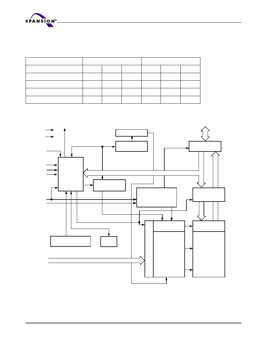
MCP Block Diagram
V
SS
RESET#
Flash
IO
15
-IO
0
V
CC
f
DQ
15
to DQ
0
RY/BY#
WP#/ACC
V
CC
V
CC
CE#
Flash-only Address
Shared Address
OE#
WE#
V
CCS
V
CC
CE#s
UB#s
LB#s
CE#
UB#
LB#
pSRAM/SRAM
CE2
8
S71GL032A Based MCPs
S71GL032A_00_A0 March 31, 2005
A d v a n c e I n f o r m a t i o n
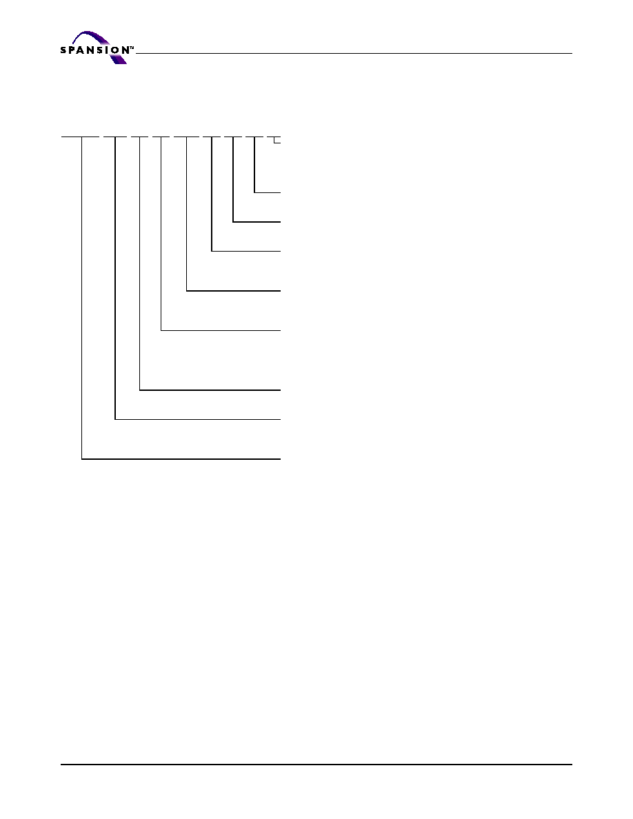
Connection Diagram (S71GL032A)
Notes:
1. May be shared depending on density.
-- A18 is shared for the 8M (p)SRAM and above configurations.
MCP
Flash-only Addresses
Shared Addresses
S71GL032A80
A20-A19
A18-A0
S71GL032A08
A20-A19
A18-A0
S71GL032A40
A20-A18
A17-A0
C3
UB#
D3
A18
E3
A17
F3
DQ1
G3
DQ9
H3
DQ10
DQ2
B3
LB#
C5
CE2s
A20
G5
DQ4
H5
VCCs
RFU
B5
WE#
C6
A19
D6
A9
E6
A10
F6
DQ6
G6
DQ13
H6
DQ12
DQ5
B6
A8
C4
RST#f
RY/BY#
G4
DQ3
H4
VCCf
DQ11
B4
WP/ACC
C7
A12
D7
A13
E7
A14
F7
RFU
G7
DQ15
H7
DQ7
DQ14
B7
A11
C8
A15
D8
RFU
E8
RFU
F8
A16
G8
RFU
VSS
C2
A6
D2
A5
E2
A4
F2
VSS
G2
OE#
H2
DQ0
CE1#s
DQ8
B2
A7
C1
A3
D1
A2
E1
A1
F1
A0
G1
CE1#f
F5
F4
B1
B8
A3
A5
A6
A4
A7
A2
RAM only
Shared
(Note 1)
Flash only
Legend
Reserved for
Future Use
56-ball Fine-Pitch Ball Grid Array
(Top View, Balls Facing Down)

March 31, 2005 S71GL032A_00_A0
S71GL032A Based MCPs
9
A d v a n c e I n f o r m a t i o n
Pin Description
A20≠A0
=
21 Address Inputs (Common and Flash only)
DQ15≠DQ0
=
16 Data Inputs/Outputs (Common)
CE#f
=
Chip Enable (Flash)
CE#ps
=
Chip Enable 1 (pSRAM)
OE#
=
Output Enable (Common)
WE#
=
Write Enable (Common)
RY/BY#
=
Ready/Busy Output (Flash 1)
UB#
=
Upper Byte Control (pSRAM/SRAM)
LB#
=
Lower Byte Control (pSRAM/SRAM)
RESET#
=
Hardware Reset Pin, Active Low (Flash)
WP#/ACC
=
Hardware Write Protect/Acceleration Pin (Flash)
V
CC
f
=
Flash 3.0 volt-only single power supply (see Product
Selector Guide for speed options and voltage supply
tolerances)
V
CC
ps
=
pSRAM/SRAM Power Supply
V
SS
=
Device Ground (Common)
NC
=
Pin Not Connected Internally
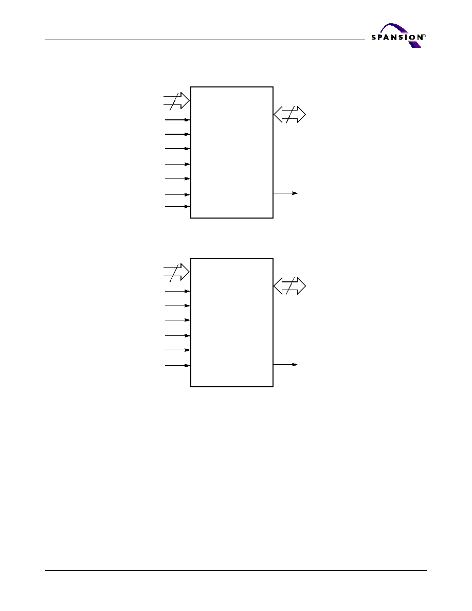
Logic Symbol
21
16
DQ15≠DQ0
A20≠A0
CE1#f
OE#
WE#
RES ET#
R Y/BY#
WP #/ACC
UB#
CE2#f
CE2ps
CE1#ps
LB#
10
S71GL032A_00A0 March 31, 2005
A d v a n c e I n f o r m a t i o n
Ordering Information
The order number is formed by a valid combinations of the following:
S71GL
032
A
80
BA
W
0
F
0
PACKING TYPE
0
= Tray
2
= 7" Tape and Reel
3
= 13" Tape and Reel
MODEL NUMBER
See the Valid Combinations table.
PACKAGE MODIFIER
0
= 7 x 9 mm, 1.2 mm height, 56 balls (TLC056)
TEMPERATURE RANGE
W
= Wireless (-25
∞
C to +85
∞
C)
I
= Industrial (-40
∞
C to +85
∞
C)
PACKAGE TYPE
BA
= Fine-pitch BGA Lead (Pb)-free compliant package
BF
= Fine-pitch BGA Lead (Pb)-free package
pSRAM DENSITY
80
= 8 Mb pSRAM
40
= 4 Mb pSRAM
08
= 8 Mb SRAM
04
= 4 Mb SRAM
PROCESS TECHNOLOGY
A
= 200 nm, MirrorBit Technology
FLASH DENSITY
064
= 64Mb
032
= 32Mb
PRODUCT FAMILY
S71GL Multi-chip Product (MCP)
3.0-volt Page Mode Flash Memory and RAM
March 31, 2005 S71GL032A_00A0
11
A d v a n c e I n f o r m a t i o n
Notes:
1. Type 0 is standard. Specify other options as required.
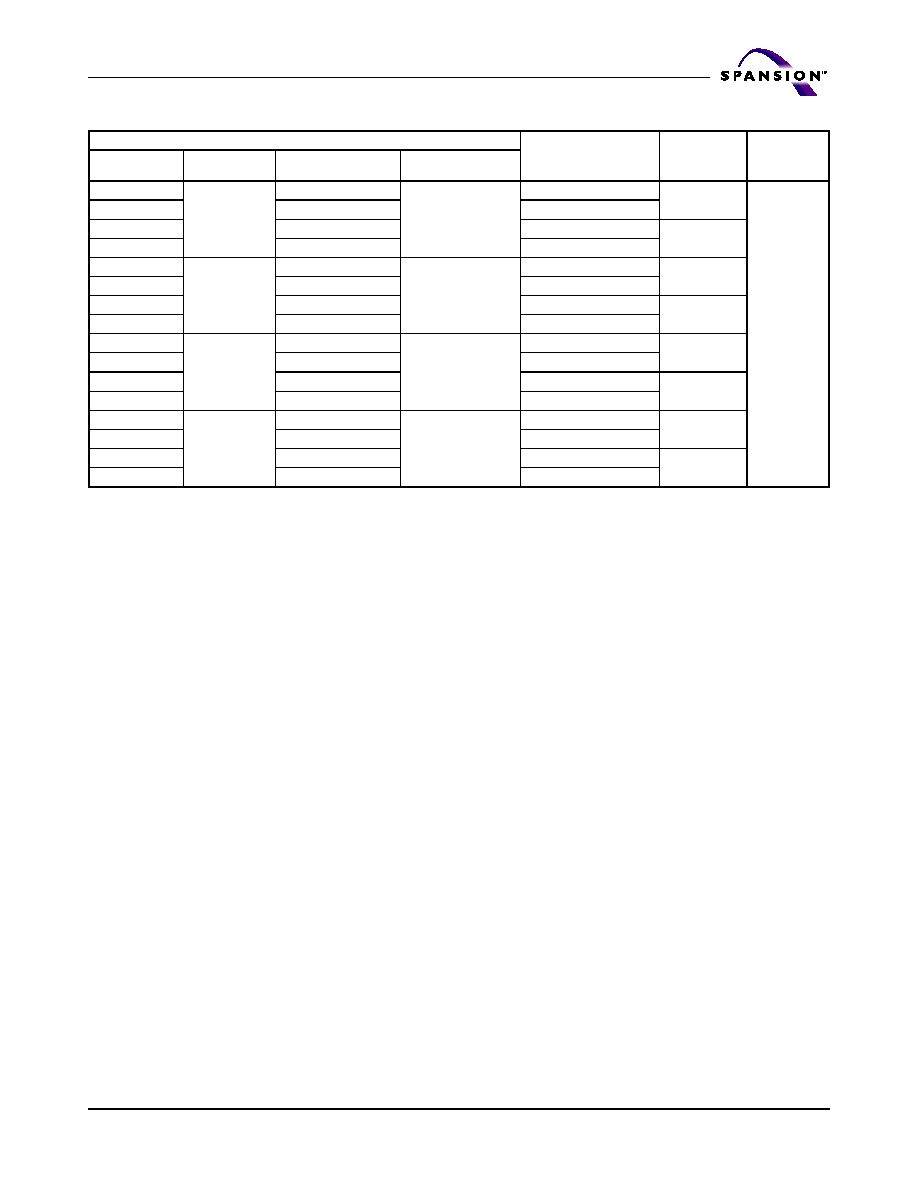
Valid Combinations
Valid Combinations list configurations planned to be supported in volume for this device.
Consult your local sales office to confirm availability of specific valid combinations and to
check on newly released combinations.
S71GL032A Valid Combinations
Speed Options (ns)/
Boot Sector Option
(p)SRAM
Type/Access
Time (ns)
Package
Marking
Base Ordering
Part Number
Package &
Temperature
Package Modifier/
Model Number
Packing Type
S71GL032A40
BAW
0B
0, 2, 3 (Note 1)
100 / Bottom Boot Sector
pSRAM4/ 70
TLC056
S71GL032A40
0F
100 / Top Boot Sector
S71GL032A08
0B
100 / Bottom Boot Sector
SRAM1 / 70
S71GL032A08
0F
100 / Top Boot Sector
S71GL032A40
BFW
0B
0, 2, 3 (Note 1)
100 / Bottom Boot Sector
pSRAM4/ 70
S71GL032A40
0F
100 / Top Boot Sector
S71GL032A08
0B
100 / Bottom Boot Sector
SRAM1 / 70
S71GL032A08
0F
100 / Top Boot Sector
S71GL032A40
BAI
0B
0, 2, 3 (Note 1)
100 / Bottom Boot Sector
pSRAM4/ 70
S71GL032A40
0F
100 / Top Boot Sector
S71GL032A08
0B
100 / Bottom Boot Sector
SRAM1 / 70
S71GL032A08
0F
100 / Top Boot Sector
S71GL032A40
BFI
0B
0, 2, 3 (Note 1)
100 / Bottom Boot Sector
pSRAM4/ 70
S71GL032A40
0F
100 / Top Boot Sector
S71GL032A08
0B
100 / Bottom Boot Sector
SRAM1 / 70
S71GL032A08
0F
100 / Top Boot Sector
12
S71GL032A Based MCPs
S71GL032A_00_A0 March 31, 2005
A d v a n c e I n f o r m a t i o n
Physical Dimensions
TLC056--56-ball Fine-Pitch Ball Grid Array (FBGA)
9 x 7 mm Package
3348 \ 16-038.22a
PACKAGE
TLC 056
JEDEC
N/A
D x E
9.00 mm x 7.00 mm
PACKAGE
SYMBOL
MIN
NOM
MAX
NOTE
A
---
---
1.20
PROFILE
A1
0.20
---
---
BALL HEIGHT
A2
0.81
---
0.97
BODY THICKNESS
D
9.00 BSC.
BODY SIZE
E
7.00 BSC.
BODY SIZE
D1
5.60 BSC.
MATRIX FOOTPRINT
E1
5.60 BSC.
MATRIX FOOTPRINT
MD
8
MATRIX SIZE D DIRECTION
ME
8
MATRIX SIZE E DIRECTION
n
56
BALL COUNT
b
0.35
0.40
0.45
BALL DIAMETER
eE
0.80 BSC.
BALL PITCH
eD
0.80 BSC
BALL PITCH
SD / SE
0.40 BSC.
SOLDER BALL PLACEMENT
A1,A8,D4,D5,E4,E5,H1,H8
DEPOPULATED SOLDER BALLS
NOTES:
1.
DIMENSIONING AND TOLERANCING METHODS PER
ASME Y14.5M-1994.
2.
ALL DIMENSIONS ARE IN MILLIMETERS.
3.
BALL POSITION DESIGNATION PER JESD 95-1, SPP-010.
4.
e REPRESENTS THE SOLDER BALL GRID PITCH.
5.
SYMBOL "MD" IS THE BALL MATRIX SIZE IN THE "D"
DIRECTION.
SYMBOL "ME" IS THE BALL MATRIX SIZE IN THE
"E" DIRECTION.
n IS THE NUMBER OF POPULTED SOLDER BALL POSITIONS
FOR MATRIX SIZE MD X ME.
6
DIMENSION "b" IS MEASURED AT THE MAXIMUM BALL
DIAMETER IN A PLANE PARALLEL TO DATUM C.
7
SD AND SE ARE MEASURED WITH RESPECT TO DATUMS A
AND B AND DEFINE THE POSITION OF THE CENTER SOLDER
BALL IN THE OUTER ROW.
WHEN THERE IS AN ODD NUMBER OF SOLDER BALLS IN THE
OUTER ROW SD OR SE = 0.000.
WHEN THERE IS AN EVEN NUMBER OF SOLDER BALLS IN THE
OUTER ROW, SD OR SE = e/2
8.
"+" INDICATES THE THEORETICAL CENTER OF DEPOPULATED
BALLS.
9.
N/A
10 A1 CORNER TO BE IDENTIFIED BY CHAMFER, LASER OR INK
MARK, METALLIZED MARK INDENTATION OR OTHER MEANS.
E1
7
SE
A
D1
eD
D
C
E
F
G
H
8
7
6
4
3
2
1
eE
5
B
PIN A1
CORNER
7
SD
BOTTOM VIEW
C
0.08
0.20 C
A
E
B
C
0.15
(2X)
C
D
C
0.15
(2X)
INDEX MARK
10
6
b
TOP VIEW
SIDE VIEW
CORNER
56X
A1
A2
A
0.15 M
M
C
C
A B
0.08
PIN A1

This document contains information on one or more products under development at Spansion LLC. The information is intended to help you evaluate this product. Do not
design in this product without contacting the factory. Spansion LLC reserves the right to change or discontinue work on this proposed product without notice.
Publication Number S71GL032A_00 Revision A Amendment 0 Issue Date March 31, 2005
ADVANCE
INFORMATION
S29GL-A MirrorBitTM Flash Family
S29GL064A, S29GL032A
64 Megabit, 32 Megabit 3.0, Volt-only Page Mode Flash
Memory Featuring 200 nm MirrorBit Process Technology
Data Sheet
Distinctive Characteristics
Architectural Advantages
Single power supply operation
-- 3 volt read, erase, and program operations
Manufactured on 200 nm MirrorBit process
technology
Secured Silicon Sector region
-- 128-word/256-byte sector for permanent, secure
identification through an 8-word/16-byte random
Electronic Serial Number, accessible through a
command sequence
-- May be programmed and locked at the factory or by
the customer
Flexible sector architecture
-- 64Mb (uniform sector models): 128 32 Kword (64 KB)
sectors
-- 64Mb (boot sector models): 127 32 Kword (64 KB)
sectors + 8 4Kword (8KB) boot sectors
-- 32Mb (uniform sector models): 64 32Kword (64KB)
sectors
-- 32Mb (boot sector models): 63 32Kword (64KB)
sectors + 8 4Kword (8KB) boot sectors
Compatibility with JEDEC standards
-- Provides pinout and software compatibility for single-
power supply flash, and superior inadvertent write
protection
100,000 erase cycles typical per sector
20-year data retention typical
Performance Characteristics
High performance
-- 90 ns access time
-- 4-word/8-byte page read buffer
-- 25 ns page read times
-- 16-word/32-byte write buffer which reduces overall
programming time for multiple-word updates
Low power consumption (typical values at 3.0 V, 5
MHz)
-- 18 mA typical active read current
-- 50 mA typical erase/program current
-- 1 µA typical standby mode current
Software & Hardware Features
Software features
-- Program Suspend & Resume: read other sectors
before programming operation is completed
-- Erase Suspend & Resume: read/program other
sectors before an erase operation is completed
-- Data# polling & toggle bits provide status
-- CFI (Common Flash Interface) compliant: allows host
system to identify and accommodate multiple flash
devices
-- Unlock Bypass Program command reduces overall
multiple-word programming time
Hardware features
-- Sector Group Protection: hardware-level method of
preventing write operations within a sector group
-- Temporary Sector Unprotect: V
ID
-level method of
charging code in locked sectors
-- WP#/ACC input accelerates programming time
(when high voltage is applied) for greater throughput
during system production. Protects first or last sector
regardless of sector protection settings on uniform
sector models
-- Hardware reset input (RESET#) resets device
-- Ready/Busy# output (RY/BY#) detects program or
erase cycle completion

14
S71GL032A Based MCPs
S71GL032A_00_A0 March 31, 2005
A d v a n c e I n f o r m a t i o n
General Description
The S29GL-A family of devices are 3.0 V single power Flash memory manufac-
tured using 200 nm MirrorBit technology. The S29GL064A is a 64 Mb, organized
as 4,194,304 words or 8,388,608 bytes. The S29GL032A is a 32 Mb, organized
as 2,097,152 words or 4,194,304 bytes. Depending on the model number, the
devices have an 8-bit wide data bus only, 16-bit wide data bus only, or a 16-bit
wide data bus that can also function as an 8-bit wide data bus by using the BYTE#
input. The devices can be programmed either in the host system or in standard
EPROM programmers.
Access times as fast as 90 ns are available. Note that each access time has a spe-
cific operating voltage range (V
CC
) as specified in the
Product Selector Guide
and
the
Ordering Information
sections. Package offerings include 48-pin TSOP, 56-pin
TSOP, 48-ball fine-pitch BGA and 64-ball Fortified BGA, depending on model num-
ber. Each device has separate chip enable (CE#), write enable (WE#) and output
enable (OE#) controls.
Each device requires only a single 3.0 volt power supply for both read and
write functions. In addition to a V
CC
input, a high-voltage accelerated program
(ACC) feature provides shorter programming times through increased current on
the WP#/ACC input. This feature is intended to facilitate factory throughput dur-
ing system production, but may also be used in the field if desired.
The device is entirely command set compatible with the JEDEC single-power-
supply Flash standard. Commands are written to the device using standard mi-
croprocessor write timing. Write cycles also internally latch addresses and data
needed for the programming and erase operations.
The sector erase architecture allows memory sectors to be erased and repro-
grammed without affecting the data contents of other sectors. The device is fully
erased when shipped from the factory.
Device programming and erasure are initiated through command sequences.
Once a program or erase operation has begun, the host system need only poll the
DQ7 (Data# Polling) or DQ6 (toggle) status bits or monitor the Ready/Busy#
(RY/BY#) output to determine whether the operation is complete. To facilitate
programming, an Unlock Bypass mode reduces command sequence overhead
by requiring only two write cycles to program data instead of four.
Hardware data protection measures include a low V
CC
detector that automat-
ically inhibits write operations during power transitions. The hardware sector
protection feature disables both program and erase operations in any combina-
tion of sectors of memory. This can be achieved in-system or via programming
equipment.
The Erase Suspend/Erase Resume feature allows the host system to pause an
erase operation in a given sector to read or program any other sector and then
complete the erase operation. The Program Suspend/Program Resume fea-
ture enables the host system to pause a program operation in a given sector to
read any other sector and then complete the program operation.
The hardware RESET# pin terminates any operation in progress and resets the
device, after which it is then ready for a new operation. The RESET# pin may be
tied to the system reset circuitry. A system reset would thus also reset the device,
enabling the host system to read boot-up firmware from the Flash memory
device.

March 31, 2005 S71GL032A_00_A0
S71GL032A Based MCPs
15
A d v a n c e I n f o r m a t i o n
The device reduces power consumption in the standby mode when it detects
specific voltage levels on CE# and RESET#, or when addresses have been stable
for a specified period of time.
The Write Protect (WP#) feature protects the first or last sector by asserting
a logic low on the WP#/ACC pin or WP# pin, depending on model number. The
protected sector will still be protected even during accelerated programming.
The Secured Silicon Sector provides a 128-word/256-byte area for code or
data that can be permanently protected. Once this sector is protected, no further
changes within the sector can occur.
Spansion MirrorBit flash technology combines years of Flash memory manufac-
turing experience to produce the highest levels of quality, reliability and cost
effectiveness. The device electrically erases all bits within a sector simultaneously
via hot-hole assisted erase. The data is programmed using hot electron injection.
16
S71GL032A Based MCPs
S71GL032A_00_A0 March 31, 2005
A d v a n c e I n f o r m a t i o n
Product Selector Guide
S29GL064A, S29GL032A
Block Diagram
Note:
**A
MAX
GL064A = A21.
**A
MAX
GL032A = A20.
Part Number
S29GL064A
S29GL032A
Speed Option
90
10
11
90
10
11
Max. Access Time (ns)
90
100
110
90
100
110
Max. CE# Access Time (ns)
90
100
110
90
100
110
Max. Page Access Time (ns)
25
30
30
25
30
30
Max. OE# Access Time (ns)
25
30
30
25
30
30
Input/Output
Buffers
X-Decoder
Y-Decoder
Chip Enable
Output Enable
Logic
Erase Voltage
Generator
PGM Voltage
Generator
Timer
V
CC
Detector
State
Control
Command
Register
V
CC
V
SS
WE#
WP#/ACC
BYTE#
CE#
OE#
STB
STB
DQ15
≠
DQ0 (A-1)
Sector Switches
RY/BY#
RESET#
Data
Latch
Y-Gating
Cell Matrix
Addr
ess L
a
tc
h
A
Max
**≠A0

March 31, 2005 S71GL032A_00_A0
S71GL032A Based MCPs
17
A d v a n c e I n f o r m a t i o n
Pin Descriptions
A21≠A0
=
22 Address inputs
A20≠A0
=
21 Address inputs
DQ7≠DQ0
=
8 Data inputs/outputs
DQ14≠DQ0
=
15 Data inputs/outputs
DQ15/A-1
=
DQ15 (Data input/output, word mode), A-1 (LSB
Address input, byte mode)
CE#
=
Chip Enable input
OE#
=
Output Enable input
WE#
=
Write Enable input
WP#/ACC
=
Hardware Write Protect input/Programming
Acceleration input
ACC
=
Acceleration input
WP#
=
Hardware Write Protect input
RESET#
=
Hardware Reset Pin input
RY/BY#
=
Ready/Busy output
BYTE#
=
Selects 8-bit or 16-bit mode
V
CC
=
3.0 volt-only single power supply
(see Product Selector Guide for speed options and
voltage supply tolerances)
V
SS
=
Device Ground
NC
=
Pin Not Connected Internally
V
IO
=
Output Buffer Power

18
S71GL032A Based MCPs
S71GL032A_00_A0 March 31, 2005
A d v a n c e I n f o r m a t i o n
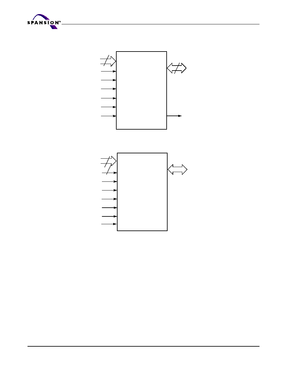
Logic Symbol-S29GL032A (Models R1, R2)
Logic Symbol-S29GL032A (Models R3, R4)
21
16
DQ15≠DQ0
(A-1)
A20≠A0
CE#
OE#
WE#
RESET#
RY/BY#
WP#/ACC
BYTE#
V
IO
21
16
DQ15≠DQ0
(A-1)
A20≠A0
CE#
OE#
WE#
RESET#
RY/BY#
WP#/ACC
BYTE#
March 31, 2005 S71GL032A_00_A0
S71GL032A Based MCPs
19
A d v a n c e I n f o r m a t i o n
Logic Symbol-S29GL064A (Models R1, R2, R8, R9)
Logic Symbol-S29GL064A (Models R3, R4)
22
16
DQ15≠DQ0
(A-1)
A21≠A0
CE#
OE#
WE#
RESET#
RY/BY#
WP#/ACC
BYTE#
V
IO
22
16
DQ15≠DQ0
(A-1)
A21≠A0
CE#
OE#
WE#
RESET#
RY/BY#
WP#/ACC
BYTE#
20
S71GL032A Based MCPs
S71GL032A_00_A0 March 31, 2005
A d v a n c e I n f o r m a t i o n
Logic Symbol-S29GL064A (Model R5)
Logic Symbol-S29GL064A (Model R6, R7)
22
16
DQ15≠DQ0
A21≠A0
CE#
OE#
WE#
RESET#
RY/BY#
ACC
V
IO
22
16
DQ15≠DQ0
A21≠A0
CE#
OE#
WE#
RESET#
ACC
WP#
V
IO
March 31, 2005 S71GL032A_00_A0
S71GL032A Based MCPs
21
A d v a n c e I n f o r m a t i o n
Device Bus Operations
This section describes the requirements and use of the device bus operations,
which are initiated through the internal command register. The command register
itself does not occupy any addressable memory location. The register is a latch
used to store the commands, along with the address and data information
needed to execute the command. The contents of the register serve as inputs to
the internal state machine. The state machine outputs dictate the function of the
device.
Table 1
lists the device bus operations, the inputs and control levels they
require, and the resulting output. The following subsections describe each of
these operations in further detail.
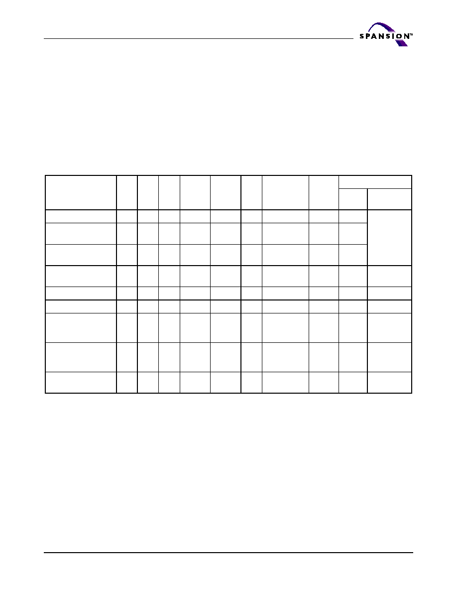
Table 1. Device Bus Operations
Legend: L = Logic Low = V
IL
, H = Logic High = V
IH
, V
ID
= 11.5≠12.5 V, V
HH
= 11.5≠12.5 V, X = Don't Care, SA = Sector
Address, A
IN
= Address In, D
IN
= Data In, D
OUT
= Data Out
Notes:
1. Addresses are Amax:A0 in word mode; Amax:A-1 in byte mode. Sector addresses are Amax:A15 in both modes.
2. The sector protect and sector unprotect functions may also be implemented via programming equipment. See the
"Sector Group Protection and Unprotection" section.
3. If WP# = V
IL
, the first or last sector remains protected (for uniform sector devices), and the two outer boot sectors
are protected (for boot sector devices). If WP# = V
IH
, the first or last sector, or the two outer boot sectors will be
protected or unprotected as determined by the method described in "Sector Group Protection and Unprotection".
All sectors are unprotected when shipped from the factory (The Secured Silicon Sector may be factory protected
depending on version ordered.)
4. D
IN
or D
OUT
as required by command sequence, data polling, or sector protect algorithm (see
Figure 7
).
Operation
CE# OE# WE# RESET#
WP#
ACC
Addresses
(Note 1)
DQ0≠
DQ7
DQ8≠DQ15
BYTE#
= V
IH
BYTE#
= V
IL
Read
L
L
H
H
X
X
A
IN
D
OUT
D
OUT
DQ8≠DQ14
= High-Z,
DQ15 = A-1
Write (Program/Erase)
L
H
L
H
(Note 3)
X
A
IN
(Note 4)
(Note
4)
Accelerated Program
L
H
L
H
(Note 3) V
HH
A
IN
(Note 4)
(Note
4)
Standby
V
CC
±
0.3 V
X
X
V
CC
±
0.3 V
X
H
X
High-Z
High-Z
High-Z
Output Disable
L
H
H
H
X
X
X
High-Z
High-Z
High-Z
Reset
X
X
X
L
X
X
X
High-Z
High-Z
High-Z
Sector Group Protect
(Note 2)
L
H
L
V
ID
H
X
SA, A6 =L,
A3=L, A2=L,
A1=H, A0=L
(Note 4)
X
X
Sector Group
Unprotect
(Note 2)
L
H
L
V
ID
H
X
SA, A6=H,
A3=L, A2=L,
A1=H, A0=L
(Note 4)
X
X
Temporary Sector
Group Unprotect
X
X
X
V
ID
H
X
A
IN
(Note 4)
(Note
4)
High-Z

22
S71GL032A Based MCPs
S71GL032A_00_A0 March 31, 2005
A d v a n c e I n f o r m a t i o n
Word/Byte Configuration
The BYTE# pin controls whether the device data I/O pins operate in the byte or
word configuration. If the BYTE# pin is set at logic `1', the device is in word con-
figuration, DQ0≠DQ15 are active and controlled by CE# and OE#.
Requirements for Reading Array Data
To read array data from the outputs, the system must drive the CE# and OE#
pins to V
IL
. CE# is the power control and selects the device. OE# is the output
control and gates array data to the output pins. WE# should remain at V
IH
.
The internal state machine is set for reading array data upon device power-up,
or after a hardware reset. This ensures that no spurious alteration of the memory
content occurs during the power transition. No command is necessary in this
mode to obtain array data. Standard microprocessor read cycles that assert valid
addresses on the device address inputs produce valid data on the device data
outputs. The device remains enabled for read access until the command register
contents are altered.
See "Reading Array Data" for more information. Refer to the AC Read-Only Op-
erations table for timing specifications and the timing diagram. Refer to the DC
Characteristics table for the active current specification on reading array data.
Page Mode Read
The device is capable of fast page mode read and is compatible with the page
mode Mask ROM read operation. This mode provides faster read access speed for
random locations within a page. The page size of the device is 4 words/8 bytes.
The appropriate page is selected by the higher address bits A(max)≠A2. Address
bits A1≠A0 in word mode (A1≠A-1 in byte mode) determine the specific word
within a page. This is an asynchronous operation; the microprocessor supplies
the specific word location.
The random or initial page access is equal to t
ACC
or t
CE
and subsequent page
read accesses (as long as the locations specified by the microprocessor falls
within that page) is equivalent to t
PACC
. When CE# is deasserted and reasserted
for a subsequent access, the access time is t
ACC
or t
CE
. Fast page mode accesses
are obtained by keeping the "read-page addresses" constant and changing the
"intra-read page" addresses.
Writing Commands/Command Sequences
To write a command or command sequence (which includes programming data
to the device and erasing sectors of memory), the system must drive WE# and
CE# to V
IL
, and OE# to V
IH
.
The device features an Unlock Bypass mode to facilitate faster programming.
Once the device enters the Unlock Bypass mode, only two write cycles are re-
quired to program a word, instead of four. The "Word Program Command
Sequence" section has details on programming data to the device using both
standard and Unlock Bypass command sequences.
An erase operation can erase one sector, multiple sectors, or the entire device.
Table 2
-
Table 17
indicates the address space that each sector occupies.
Refer to the DC Characteristics table for the active current specification for the
write mode. The AC Characteristics section contains timing specification tables
and timing diagrams for write operations.

March 31, 2005 S71GL032A_00_A0
S71GL032A Based MCPs
23
A d v a n c e I n f o r m a t i o n
Write Buffer
Write Buffer Programming allows the system write to a maximum of 16 in one
programming operation. This results in faster effective programming time than
the standard programming algorithms. See "Write Buffer" for more information.
Accelerated Program Operation
The device offers accelerated program operations through the ACC function. This
is one of two functions provided by the WP#/ACC or ACC pin, depending on model
number. This function is primarily intended to allow faster manufacturing
throughput at the factory.
If the system asserts V
HH
on this pin, the device automatically enters the afore-
mentioned Unlock Bypass mode, temporarily unprotects any protected sector
groups, and uses the higher voltage on the pin to reduce the time required for
program operations. The system would use a two-cycle program command se-
quence as required by the Unlock Bypass mode. Removing V
HH
from the WP#/
ACC or ACC pin, depending on model number, returns the device to normal op-
eration. Note that the WP#/ACC or ACC pin must not be at V
HH
for operations
other than accelerated programming, or device damage may result. WP# has an
internal pullup; when unconnected, WP# is at V
IH
.
Autoselect Functions
If the system writes the autoselect command sequence, the device enters the au-
toselect mode. The system can then read autoselect codes from the internal
register (which is separate from the memory array) on DQ7≠DQ0. Standard read
cycle timings apply in this mode. Refer to the
"Autoselect Mode" section on page
31
and
"Autoselect Command Sequence" section on page 45
sections for more
information.
Standby Mode
When the system is not reading or writing to the device, it can place the device
in the standby mode. In this mode, current consumption is greatly reduced, and
the outputs are placed in the high impedance state, independent of the OE#
input.
The device enters the CMOS standby mode when the CE# and RESET# pins are
both held at V
IO
± 0.3 V. (Note that this is a more restricted voltage range than
V
IH
.) If CE# and RESET# are held at V
IH
, but not within V
IO
± 0.3 V, the device
will be in the standby mode, but the standby current will be greater. The device
requires standard access time (t
CE
) for read access when the device is in either
of these standby modes, before it is ready to read data.
If the device is deselected during erasure or programming, the device draws ac-
tive current until the operation is completed.
Refer to the
"DC Characteristics" section on page 65
for the standby current
specification.
Automatic Sleep Mode
The automatic sleep mode minimizes Flash device energy consumption. The de-
vice automatically enables this mode when addresses remain stable for t
ACC
+
30 ns. The automatic sleep mode is independent of the CE#, WE#, and OE# con-
trol signals. Standard address access timings provide new data when addresses
are changed. While in sleep mode, output data is latched and always available to
24
S71GL032A Based MCPs
S71GL032A_00_A0 March 31, 2005
A d v a n c e I n f o r m a t i o n
the system. Refer to the
"DC Characteristics" section on page 65
for the
automatic sleep mode current specification.
RESET#: Hardware Reset Pin
The RESET# pin provides a hardware method of resetting the device to reading
array data. When the RESET# pin is driven low for at least a period of t
RP
, the
device immediately terminates any operation in progress, tristates all output
pins, and ignores all read/write commands for the duration of the RESET# pulse.
The device also resets the internal state machine to reading array data. The op-
eration that was interrupted should be reinitiated once the device is ready to
accept another command sequence, to ensure data integrity.
Current is reduced for the duration of the RESET# pulse. When RESET# is held
at V
SS
±0.3 V, the device draws CMOS standby current (I
CC5
). If RESET# is held
at V
IL
but not within V
SS
±0.3 V, the standby current will be greater.
The RESET# pin may be tied to the system reset circuitry. A system reset would
thus also reset the Flash memory, enabling the system to read the boot-up firm-
ware from the Flash memory.
Refer to the AC Characteristics tables for RESET# parameters and to
Figure 15
for the timing diagram.
Output Disable Mode
When the OE# input is at V
IH
, output from the device is disabled. The output pins
are placed in the high impedance state.
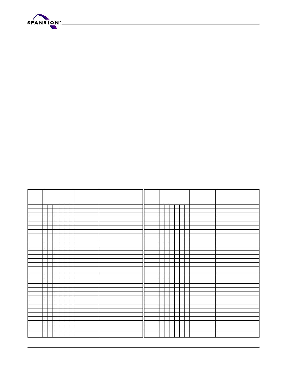
Table 2. S29GL032M (Models R1, R2) Sector Addresses
Sec
t
or
A20-A15
Sector
Size
(KB/
Kwords)
16-bit
Address
Range
Sec
t
or
A20-A15
Sector
Size
(KB/
Kwords)
16-bit
Address
Range
SA0
0 0 0 0 0 0
64/32
000000≠007FFF
SA32
1 0 0 0 0 0
64/32
100000≠107FFF
SA1
0 0 0 0 0 1
64/32
008000≠00FFFF
SA33
1 0 0 0 0 1
64/32
108000≠10FFFF
SA2
0 0 0 0 1 0
64/32
010000≠017FFF
SA34
1 0 0 0 1 0
64/32
110000≠117FFF
SA3
0 0 0 0 1 1
64/32
018000≠01FFFF
SA35
1 0 0 0 1 1
64/32
118000≠11FFFF
SA4
0 0 0 1 0 0
64/32
020000≠027FFF
SA36
1 0 0 1 0 0
64/32
120000≠127FFF
SA5
0 0 0 1 0 1
64/32
028000≠02FFFF
SA37
1 0 0 1 0 1
64/32
128000≠12FFFF
SA6
0 0 0 1 1 0
64/32
030000≠037FFF
SA38
1 0 0 1 1 0
64/32
130000≠137FFF
SA7
0 0 0 1 1 1
64/32
038000≠03FFFF
SA39
1 0 0 1 1 1
64/32
138000≠13FFFF
SA8
0 0 1 0 0 0
64/32
040000≠047FFF
SA40
1 0 1 0 0 0
64/32
140000≠147FFF
SA9
0 0 1 0 0 1
64/32
048000≠04FFFF
SA41
1 0 1 0 0 1
64/32
148000≠14FFFF
SA10
0 0 1 0 1 0
64/32
050000≠057FFF
SA42
1 0 1 0 1 0
64/32
150000≠157FFF
SA11
0 0 1 0 1 1
64/32
058000≠05FFFF
SA43
1 0 1 0 1 1
64/32
158000≠15FFFF
SA12
0 0 1 1 0 0
64/32
060000≠067FFF
SA44
1 0 1 1 0 0
64/32
160000≠167FFF
SA13
0 0 1 1 0 1
64/32
068000≠06FFFF
SA45
1 0 1 1 0 1
64/32
168000≠16FFFF
SA14
0 0 1 1 1 0
64/32
070000≠077FFF
SA46
1 0 1 1 1 0
64/32
170000≠177FFF
SA15
0 0 1 1 1 1
64/32
078000≠07FFFF
SA47
1 0 1 1 1 1
64/32
178000≠17FFFF
SA16
0 1 0 0 0 0
64/32
080000≠087FFF
SA48
1 1 0 0 0 0
64/32
180000≠187FFF
SA17
0 1 0 0 0 1
64/32
088000≠08FFFF
SA49
1 1 0 0 0 1
64/32
188000≠18FFFF
SA18
0 1 0 0 1 0
64/32
090000≠097FFF
SA50
1 1 0 0 1 0
64/32
190000≠197FFF
SA19
0 1 0 0 1 1
64/32
098000≠09FFFF
SA51
1 1 0 0 1 1
64/32
198000≠19FFFF
SA20
0 1 0 1 0 0
64/32
0A0000≠0A7FFF
SA52
1 1 0 1 0 0
64/32
1A0000≠1A7FFF
SA21
0 1 0 1 0 1
64/32
0A8000≠0AFFFF
SA53
1 1 0 1 0 1
64/32
1A8000≠1AFFFF
SA22
0 1 0 1 1 0
64/32
0B0000≠0B7FFF
SA54
1 1 0 1 1 0
64/32
1B0000≠1B7FFF
SA23
0 1 0 1 1 1
64/32
0B8000≠0BFFFF
SA55
1 1 0 1 1 1
64/32
1B8000≠1BFFFF
SA24
0 1 1 0 0 0
64/32
0C0000≠0C7FFF
SA56
1 1 1 0 0 0
64/32
1C0000≠1C7FFF
SA25
0 1 1 0 0 1
64/32
0C8000≠0CFFFF
SA57
1 1 1 0 0 1
64/32
1C8000≠1CFFFF
SA26
0 1 1 0 1 0
64/32
0D0000≠0D7FFF
SA58
1 1 1 0 1 0
64/32
1D0000≠1D7FFF
SA27
0 1 1 0 1 1
64/32
0D8000≠0DFFFF
SA59
1 1 1 0 1 1
64/32
1D8000≠1DFFFF
SA28
0 1 1 1 0 0
64/32
0E0000≠0E7FFF
SA60
1 1 1 1 0 0
64/32
1E0000≠1E7FFF
SA29
0 1 1 1 0 1
64/32
0E8000≠0EFFFF
SA61
1 1 1 1 0 1
64/32
1E8000≠1EFFFF
SA30
0 1 1 1 1 0
64/32
0F0000≠0F7FFF
SA62
1 1 1 1 1 0
64/32
1F0000≠1F7FFF
SA31
0 1 1 1 1 1
64/32
0F8000≠0FFFFF
SA63
1 1 1 1 1 1
64/32
1F8000≠1FFFFF
March 31, 2005 S71GL032A_00_A0
S71GL032A Based MCPs
25
A d v a n c e I n f o r m a t i o n
Table 3. S29GL032M (Models R3) Top Boot Sector Addresses
Sec
t
or
A20≠A12
Sector
Size
(KB/
Kwords)
16-bit
Address
Range
Sec
t
or
A20≠A12
Sector
Size
(KB/
Kwords)
16-bit
Address
Range
SA0
000000xxx
64/32
00000h≠07FFFh
SA36
100100xxx
64/32
120000h≠127FFFh
SA1
000001xxx
64/32
08000h≠0FFFFh
SA37
100101xxx
64/32
128000h≠12FFFFh
SA2
000010xxx
64/32
10000h≠17FFFh
SA38
100110xxx
64/32
130000h≠137FFFh
SA3
000011xxx
64/32
18000h≠1FFFFh
SA39
100111xxx
64/32
138000h≠13FFFFh
SA4
000100xxx
64/32
20000h≠27FFFh
SA40
101000xxx
64/32
140000h≠147FFFh
SA5
000101xxx
64/32
28000h≠2FFFFh
SA41
101001xxx
64/32
148000h≠14FFFFh
SA6
000110xxx
64/32
30000h≠37FFFh
SA42
101010xxx
64/32
150000h≠157FFFh
SA7
000111xxx
64/32
38000h≠3FFFFh
SA43
101011xxx
64/32
158000h≠15FFFFh
SA8
001000xxx
64/32
40000h≠47FFFh
SA44
101100xxx
64/32
160000h≠167FFFh
SA9
001001xxx
64/32
48000h≠4FFFFh
SA45
101101xxx
64/32
168000h≠16FFFFh
SA10
001010xxx
64/32
50000h≠57FFFh
SA46
101110xxx
64/32
170000h≠177FFFh
SA11
001011xxx
64/32
58000h≠5FFFFh
SA47
101111xxx
64/32
178000h≠17FFFFh
SA12
001100xxx
64/32
60000h≠67FFFh
SA48
110000xxx
64/32
180000h≠187FFFh
SA13
001101xxx
64/32
68000h≠6FFFFh
SA49
110001xxx
64/32
188000h≠18FFFFh
SA14
001101xxx
64/32
70000h≠77FFFh
SA50
110010xxx
64/32
190000h≠197FFFh
SA15
001111xxx
64/32
78000h≠7FFFFh
SA51
110011xxx
64/32
198000h≠19FFFFh
SA16
010000xxx
64/32
80000h≠87FFFh
SA52
100100xxx
64/32
1A0000h≠1A7FFFh
SA17
010001xxx
64/32
88000h≠8FFFFh
SA53
110101xxx
64/32
1A8000h≠1AFFFFh
SA18
010010xxx
64/32
90000h≠97FFFh
SA54
110110xxx
64/32
1B0000h≠1B7FFFh
SA19
010011xxx
64/32
98000h≠9FFFFh
SA55
110111xxx
64/32
1B8000h≠1BFFFFh
SA20
010100xxx
64/32
A0000h≠A7FFFh
SA56
111000xxx
64/32
1C0000h≠1C7FFFh
SA21
010101xxx
64/32
A8000h≠AFFFFh
SA57
111001xxx
64/32
1C8000h≠1CFFFFh
SA22
010110xxx
64/32
B0000h≠B7FFFh
SA58
111010xxx
64/32
1D0000h≠1D7FFFh
SA23
010111xxx
64/32
B8000h≠BFFFFh
SA59
111011xxx
64/32
1D8000h≠1DFFFFh
SA24
011000xxx
64/32
C0000h≠C7FFFh
SA60
111100xxx
64/32
1E0000h≠1E7FFFh
SA25
011001xxx
64/32
C8000h≠CFFFFh
SA61
111101xxx
64/32
1E8000h≠1EFFFFh
SA26
011010xxx
64/32
D0000h≠D7FFFh
SA62
111110xxx
64/32
1F0000h≠1F7FFFh
SA27
011011xxx
64/32
D8000h≠DFFFFh
SA63
111111000
8/4
1F8000h≠1F8FFFh
SA28
011000xxx
64/32
E0000h≠E7FFFh
SA64
111111001
8/4
1F9000h≠1F9FFFh
SA29
011101xxx
64/32
E8000h≠EFFFFh
SA65
111111010
8/4
1FA000h≠1FAFFFh
SA30
011110xxx
64/32
F0000h≠F7FFFh
SA66
111111011
8/4
1FB000h≠1FBFFFh
SA31
011111xxx
64/32
F8000h≠FFFFFh
SA67
111111100
8/4
1FC000h≠1FCFFFh
SA32
100000xxx
64/32
F9000h≠107FFFh
SA68
111111101
8/4
1FD000h≠1FDFFFh
SA33
100001xxx
64/32
108000h≠10FFFFh
SA69
111111110
8/4
1FE000h≠1FEFFFh
SA34
100010xxx
64/32
110000h≠117FFFh
SA70
111111111
8/4
1FF000h≠1FFFFFh
SA35
101011xxx
64/32
118000h≠11FFFFh
Table 4. S29GL032M (Models R4) Bottom Boot Sector Addresses (Sheet 1 of 2)
Se
c
t
or
A20≠A12
Sector
Size
(KB/
Kwords)
16-bit
Address
Range
Se
c
t
or
A20≠A12
Sector
Size
(KB/
Kwords)
16-bit
Address
Range
SA0
000000000
8/4
00000h≠00FFFh
SA19
001100xxx
64/32
60000h≠67FFFh
SA1
000000001
8/4
01000h≠01FFFh
SA20
001101xxx
64/32
68000h≠6FFFFh
SA2
000000010
8/4
02000h≠02FFFh
SA21
001101xxx
64/32
70000h≠77FFFh
SA3
000000011
8/4
03000h≠03FFFh
SA22
001111xxx
64/32
78000h≠7FFFFh
SA4
000000100
8/4
04000h≠04FFFh
SA23
010000xxx
64/32
80000h≠87FFFh
SA5
000000101
8/4
05000h≠05FFFh
SA24
010001xxx
64/32
88000h≠8FFFFh
SA6
000000110
8/4
06000h≠06FFFh
SA25
010010xxx
64/32
90000h≠97FFFh
SA7
000000111
8/4
07000h≠07FFFh
SA26
010011xxx
64/32
98000h≠9FFFFh
SA8
000001xxx
64/32
08000h≠0FFFFh
SA27
010100xxx
64/32
A0000h≠A7FFFh
SA9
000010xxx
64/32
10000h≠17FFFh
SA28
010101xxx
64/32
A8000h≠AFFFFh
SA10
000011xxx
64/32
18000h≠1FFFFh
SA29
010110xxx
64/32
B0000h≠B7FFFh
SA11
000100xxx
64/32
20000h≠27FFFh
SA30
010111xxx
64/32
B8000h≠BFFFFh
SA12
000101xxx
64/32
28000h≠2FFFFh
SA31
011000xxx
64/32
C0000h≠C7FFFh
SA13
000110xxx
64/32
30000h≠37FFFh
SA32
011001xxx
64/32
C8000h≠CFFFFh
SA14
000111xxx
64/32
38000h≠3FFFFh
SA33
011010xxx
64/32
D0000h≠D7FFFh
SA15
001000xxx
64/32
40000h≠47FFFh
SA34
011011xxx
64/32
D8000h≠DFFFFh
SA16
001001xxx
64/32
48000h≠4FFFFh
SA35
011000xxx
64/32
E0000h≠E7FFFh
SA17
001010xxx
64/32
50000h≠57FFFh
SA36
011101xxx
64/32
E8000h≠EFFFFh
SA18
001011xxx
64/32
58000h≠5FFFFh
SA37
011110xxx
64/32
F0000h≠F7FFFh
26
S71GL032A Based MCPs
S71GL032A_00_A0 March 31, 2005
A d v a n c e I n f o r m a t i o n
SA38
011111xxx
64/32
F8000h≠FFFFFh
SA55
110000xxx
64/32
180000h≠187FFFh
SA39
100000xxx
64/32
F9000h≠107FFFh
SA56
110001xxx
64/32
188000h≠18FFFFh
SA40
100001xxx
64/32
108000h≠10FFFFh
SA57
110010xxx
64/32
190000h≠197FFFh
SA41
100010xxx
64/32
110000h≠117FFFh
SA58
110011xxx
64/32
198000h≠19FFFFh
SA42
101011xxx
64/32
118000h≠11FFFFh
SA59
100100xxx
64/32
1A0000h≠1A7FFFh
SA43
100100xxx
64/32
120000h≠127FFFh
SA60
110101xxx
64/32
1A8000h≠1AFFFFh
SA44
100101xxx
64/32
128000h≠12FFFFh
SA61
110110xxx
64/32
1B0000h≠1B7FFFh
SA45
100110xxx
64/32
130000h≠137FFFh
SA62
110111xxx
64/32
1B8000h≠1BFFFFh
SA46
100111xxx
64/32
138000h≠13FFFFh
SA63
111000xxx
64/32
1C0000h≠1C7FFFh
SA47
101000xxx
64/32
140000h≠147FFFh
SA64
111001xxx
64/32
1C8000h≠1CFFFFh
SA48
101001xxx
64/32
148000h≠14FFFFh
SA65
111010xxx
64/32
1D0000h≠1D7FFFh
SA49
101010xxx
64/32
150000h≠157FFFh
SA66
111011xxx
64/32
1D8000h≠1DFFFFh
SA50
101011xxx
64/32
158000h≠15FFFFh
SA67
111100xxx
64/32
1E0000h≠1E7FFFh
SA51
101100xxx
64/32
160000h≠167FFFh
SA68
111101xxx
64/32
1E8000h≠1EFFFFh
SA52
101101xxx
64/32
168000h≠16FFFFh
SA69
111110xxx
64/32
1F0000h≠1F7FFFh
SA53
101110xxx
64/32
170000h≠177FFFh
SA70
111111xxx
64/32
1F8000h≠1FFFFFh
SA54
101111xxx
64/32
178000h≠17FFFFh
Table 5. S29GL064A (Models R1, R2, R8, R9) Sector Addresses (Sheet 1 of 2)
Sec
t
or
A21≠A15
Sector
Size
(KB/
Kwords)
16-bit
Address
Range
Sec
t
or
A21≠A15
Sector
Size
(KB/
Kwords)
16-bit
Address
Range
SA0
0000000
64/32
000000≠007FFF
SA37
0100101
64/32
128000≠12FFFF
SA1
0000001
64/32
008000≠00FFFF
SA38
0100110
64/32
130000≠137FFF
SA2
0000010
64/32
010000≠017FFF
SA39
0100111
64/32
138000≠13FFFF
SA3
0000011
64/32
018000≠01FFFF
SA40
0101000
64/32
140000≠147FFF
SA4
0000100
64/32
020000≠027FFF
SA41
0101001
64/32
148000≠14FFFF
SA5
0000101
64/32
028000≠02FFFF
SA42
0101010
64/32
150000≠157FFF
SA6
0000110
64/32
030000≠037FFF
SA43
0101011
64/32
158000≠15FFFF
SA7
0000111
64/32
038000≠03FFFF
SA44
0101100
64/32
160000≠167FFF
SA8
0001000
64/32
040000≠047FFF
SA45
0101101
64/32
168000≠16FFFF
SA9
0001001
64/32
048000≠04FFFF
SA46
0101110
64/32
170000≠177FFF
SA10
0001010
64/32
050000≠057FFF
SA47
0101111
64/32
178000≠17FFFF
SA11
0001011
64/32
058000≠05FFFF
SA48
0110000
64/32
180000≠187FFF
SA12
0001100
64/32
060000≠067FFF
SA49
0110001
64/32
188000≠18FFFF
SA13
0001101
64/32
068000≠06FFFF
SA50
0110010
64/32
190000≠197FFF
SA14
0001110
64/32
070000≠077FFF
SA51
0110011
64/32
198000≠19FFFF
SA15
0001111
64/32
078000≠07FFFF
SA52
0110100
64/32
1A0000≠1A7FFF
SA16
0010000
64/32
080000≠087FFF
SA53
0110101
64/32
1A8000≠1AFFFF
SA17
0010001
64/32
088000≠08FFFF
SA54
0110110
64/32
1B0000≠1B7FFF
SA18
0010010
64/32
090000≠097FFF
SA55
0110111
64/32
1B8000≠1BFFFF
SA19
0010011
64/32
098000≠09FFFF
SA56
0111000
64/32
1C0000≠1C7FFF
SA20
0010100
64/32
0A0000≠0A7FFF
SA57
0111001
64/32
1C8000≠1CFFFF
SA21
0010101
64/32
0A8000≠0AFFFF
SA58
0111010
64/32
1D0000≠1D7FFF
SA22
0010110
64/32
0B0000≠0B7FFF
SA59
0111011
64/32
1D8000≠1DFFFF
SA23
0010111
64/32
0B8000≠0BFFFF
SA60
0111100
64/32
1E0000≠1E7FFF
SA24
0011000
64/32
0C0000≠0C7FFF
SA61
0111101
64/32
1E8000≠1EFFFF
SA25
0011001
64/32
0C8000≠0CFFFF
SA62
0111110
64/32
1F0000≠1F7FFF
SA26
0011010
64/32
0D0000≠0D7FFF
SA63
0111111
64/32
1F8000≠1FFFFF
SA27
0011011
64/32
0D8000≠0DFFFF
SA64
1000000
64/32
200000≠207FFF
SA28
0011100
64/32
0E0000≠0E7FFF
SA65
1000001
64/32
208000≠20FFFF
SA29
0011101
64/32
0E8000≠0EFFFF
SA66
1000010
64/32
210000≠217FFF
SA30
0011110
64/32
0F0000≠0F7FFF
SA67
1000011
64/32
218000≠21FFFF
SA31
0011111
64/32
0F8000≠0FFFFF
SA68
1000100
64/32
220000≠227FFF
SA32
0100000
64/32
100000≠107FFF
SA69
1000101
64/32
228000≠22FFFF
SA33
0100001
64/32
108000≠10FFFF
SA70
1000110
64/32
230000≠237FFF
SA34
0100010
64/32
110000≠117FFF
SA71
1000111
64/32
238000≠23FFFF
SA35
0100011
64/32
118000≠11FFFF
SA72
1001000
64/32
240000≠247FFF
SA36
0100100
64/32
120000≠127FFF
SA73
1001001
64/32
248000≠24FFFF
Table 4. S29GL032M (Models R4) Bottom Boot Sector Addresses (Sheet 2 of 2)
Sec
t
or
A20≠A12
Sector
Size
(KB/
Kwords)
16-bit
Address
Range
Sec
t
or
A20≠A12
Sector
Size
(KB/
Kwords)
16-bit
Address
Range
March 31, 2005 S71GL032A_00_A0
S71GL032A Based MCPs
27
A d v a n c e I n f o r m a t i o n
SA74
1001010
64/32
250000≠257FFF
SA101
1100101
64/32
328000≠32FFFF
SA75
1001011
64/32
258000≠25FFFF
SA102
1100110
64/32
330000≠337FFF
SA76
1001100
64/32
260000≠267FFF
SA103
1100111
64/32
338000≠33FFFF
SA77
1001101
64/32
268000≠26FFFF
SA104
1101000
64/32
340000≠347FFF
SA78
1001110
64/32
270000≠277FFF
SA105
1101001
64/32
348000≠34FFFF
SA79
1001111
64/32
278000≠27FFFF
SA106
1101010
64/32
350000≠357FFF
SA80
1010000
64/32
280000≠287FFF
SA107
1101011
64/32
358000≠35FFFF
SA81
1010001
64/32
288000≠28FFFF
SA108
1101100
64/32
360000≠367FFF
SA82
1010010
64/32
290000≠297FFF
SA109
1101101
64/32
368000≠36FFFF
SA83
1010011
64/32
298000≠29FFFF
SA110
1101110
64/32
370000≠377FFF
SA84
1010100
64/32
2A0000≠2A7FFF
SA111
1101111
64/32
378000≠37FFFF
SA85
1010101
64/32
2A8000≠2AFFFF
SA112
1110000
64/32
380000≠387FFF
SA86
1010110
64/32
2B0000≠2B7FFF
SA113
1110001
64/32
388000≠38FFFF
SA87
1010111
64/32
2B8000≠2BFFFF
SA114
1110010
64/32
390000≠397FFF
SA88
1011000
64/32
2C0000≠2C7FFF
SA115
1110011
64/32
398000≠39FFFF
SA89
1011001
64/32
2C8000≠2CFFFF
SA116
1110100
64/32
3A0000≠3A7FFF
SA90
1011010
64/32
2D0000≠2D7FFF
SA117
1110101
64/32
3A8000≠3AFFFF
SA91
1011011
64/32
2D8000≠2DFFFF
SA118
1110110
64/32
3B0000≠3B7FFF
SA92
1011100
64/32
2E0000≠2E7FFF
SA119
1110111
64/32
3B8000≠3BFFFF
SA93
1011101
64/32
2E8000≠2EFFFF
SA120
1111000
64/32
3C0000≠3C7FFF
SA94
1011110
64/32
2F0000≠2F7FFF
SA121
1111001
64/32
3C8000≠3CFFFF
SA95
1011111
64/32
2F8000≠2FFFFF
SA122
1111010
64/32
3D0000≠3D7FFF
SA96
1100000
64/32
300000≠307FFF
SA123
1111011
64/32
3D8000≠3DFFFF
SA97
1100001
64/32
308000≠30FFFF
SA124
1111100
64/32
3E0000≠3E7FFF
SA98
1100010
64/32
310000≠317FFF
SA125
1111101
64/32
3E8000≠3EFFFF
SA99
1100011
64/32
318000≠31FFFF
SA126
1111110
64/32
3F0000≠3F7FFF
SA100
1100100
64/32
320000≠327FFF
SA127
1111111
64/32
3F8000≠3FFFFF
Table 6. S29GL064A (Model R3) Top Boot Sector Addresses (Sheet 1 of 2)
Sector
A21≠A15
Sector
Size
(KB/
Kwords)
16-bit
Address
Range
Sector
A21≠A15
Sector
Size
(KB/
Kwords)
16-bit
Address
Range
SA0
0000000xxx
64/32
00000h≠07FFFh
SA34
0100010xxx
64/32
110000h≠117FFFh
SA1
0000001xxx
64/32
08000h≠0FFFFh
SA35
0101011xxx
64/32
118000h≠11FFFFh
SA2
0000010xxx
64/32
10000h≠17FFFh
SA36
0100100xxx
64/32
120000h≠127FFFh
SA3
0000011xxx
64/32
18000h≠1FFFFh
SA37
0100101xxx
64/32
128000h≠12FFFFh
SA4
0000100xxx
64/32
20000h≠27FFFh
SA38
0100110xxx
64/32
130000h≠137FFFh
SA5
0000101xxx
64/32
28000h≠2FFFFh
SA39
0100111xxx
64/32
138000h≠13FFFFh
SA6
0000110xxx
64/32
30000h≠37FFFh
SA40
0101000xxx
64/32
140000h≠147FFFh
SA7
0000111xxx
64/32
38000h≠3FFFFh
SA41
0101001xxx
64/32
148000h≠14FFFFh
SA8
0001000xxx
64/32
40000h≠47FFFh
SA42
0101010xxx
64/32
150000h≠157FFFh
SA9
0001001xxx
64/32
48000h≠4FFFFh
SA43
0101011xxx
64/32
158000h≠15FFFFh
SA10
0001010xxx
64/32
50000h≠57FFFh
SA44
0101100xxx
64/32
160000h≠167FFFh
SA11
0001011xxx
64/32
58000h≠5FFFFh
SA45
0101101xxx
64/32
168000h≠16FFFFh
SA12
0001100xxx
64/32
60000h≠67FFFh
SA46
0101110xxx
64/32
170000h≠177FFFh
SA13
0001101xxx
64/32
68000h≠6FFFFh
SA47
0101111xxx
64/32
178000h≠17FFFFh
SA14
0001101xxx
64/32
70000h≠77FFFh
SA48
0110000xxx
64/32
180000h≠187FFFh
SA15
0001111xxx
64/32
78000h≠7FFFFh
SA49
0110001xxx
64/32
188000h≠18FFFFh
SA16
0010000xxx
64/32
80000h≠87FFFh
SA50
0110010xxx
64/32
190000h≠197FFFh
SA17
0010001xxx
64/32
88000h≠8FFFFh
SA51
0110011xxx
64/32
198000h≠19FFFFh
SA18
0010010xxx
64/32
90000h≠97FFFh
SA52
0100100xxx
64/32
1A0000h≠1A7FFFh
SA19
0010011xxx
64/32
98000h≠9FFFFh
SA53
0110101xxx
64/32
1A8000h≠1AFFFFh
SA20
0010100xxx
64/32
A0000h≠A7FFFh
SA54
0110110xxx
64/32
1B0000h≠1B7FFFh
SA21
0010101xxx
64/32
A8000h≠AFFFFh
SA55
0110111xxx
64/32
1B8000h≠1BFFFFh
SA22
0010110xxx
64/32
B0000h≠B7FFFh
SA56
0111000xxx
64/32
1C0000h≠1C7FFFh
SA23
0010111xxx
64/32
B8000h≠BFFFFh
SA57
0111001xxx
64/32
1C8000h≠1CFFFFh
SA24
0011000xxx
64/32
C0000h≠C7FFFh
SA58
0111010xxx
64/32
1D0000h≠1D7FFFh
SA25
0011001xxx
64/32
C8000h≠CFFFFh
SA59
0111011xxx
64/32
1D8000h≠1DFFFFh
SA26
0011010xxx
64/32
D0000h≠D7FFFh
SA60
0111100xxx
64/32
1E0000h≠1E7FFFh
SA27
0011011xxx
64/32
D8000h≠DFFFFh
SA61
0111101xxx
64/32
1E8000h≠1EFFFFh
SA28
0011000xxx
64/32
E0000h≠E7FFFh
SA62
0111110xxx
64/32
1F0000h≠1F7FFFh
SA29
0011101xxx
64/32
E8000h≠EFFFFh
SA63
0111111xxx
64/32
1F8000h≠1FFFFFh
SA30
0011110xxx
64/32
F0000h≠F7FFFh
SA64
1000000xxx
64/32
200000h≠207FFFh
SA31
0011111xxx
64/32
F8000h≠FFFFFh
SA65
1000001xxx
64/32
208000h≠20FFFFh
SA32
0100000xxx
64/32
F9000h≠107FFFh
SA66
1000010xxx
64/32
210000h≠217FFFh
SA33
0100001xxx
64/32
108000h≠10FFFFh
SA67
1000011xxx
64/32
218000h≠21FFFFh
Table 5. S29GL064A (Models R1, R2, R8, R9) Sector Addresses (Sheet 2 of 2)
Sec
t
or
A21≠A15
Sector
Size
(KB/
Kwords)
16-bit
Address
Range
Sec
t
or
A21≠A15
Sector
Size
(KB/
Kwords)
16-bit
Address
Range
28
S71GL032A Based MCPs
S71GL032A_00_A0 March 31, 2005
A d v a n c e I n f o r m a t i o n
SA68
1000100xxx
64/32
220000h≠227FFFh
SA102
1100110xxx
64/32
330000h≠337FFFh
SA69
1000101xxx
64/32
228000h≠22FFFFh
SA103
1100111xxx
64/32
338000h≠33FFFFh
SA70
1000110xxx
64/32
230000h≠237FFFh
SA104
1101000xxx
64/32
340000h≠347FFFh
SA71
1000111xxx
64/32
238000h≠23FFFFh
SA105
1101001xxx
64/32
348000h≠34FFFFh
SA72
1001000xxx
64/32
240000h≠247FFFh
SA106
1101010xxx
64/32
350000h≠357FFFh
SA73
1001001xxx
64/32
248000h≠24FFFFh
SA107
1101011xxx
64/32
358000h≠35FFFFh
SA74
1001010xxx
64/32
250000h≠257FFFh
SA108
1101100xxx
64/32
360000h≠367FFFh
SA75
1001011xxx
64/32
258000h≠25FFFFh
SA109
1101101xxx
64/32
368000h≠36FFFFh
SA76
1001100xxx
64/32
260000h≠267FFFh
SA110
1101110xxx
64/32
370000h≠377FFFh
SA77
1001101xxx
64/32
268000h≠26FFFFh
SA111
1101111xxx
64/32
378000h≠37FFFFh
SA78
1001110xxx
64/32
270000h≠277FFFh
SA112
1110000xxx
64/32
380000h≠387FFFh
SA79
1001111xxx
64/32
278000h≠27FFFFh
SA113
1110001xxx
64/32
388000h≠38FFFFh
SA80
1010000xxx
64/32
280000h≠28FFFFh
SA114
1110010xxx
64/32
390000h≠397FFFh
SA81
1010001xxx
64/32
288000h≠28FFFFh
SA115
1110011xxx
64/32
398000h≠39FFFFh
SA82
1010010xxx
64/32
290000h≠297FFFh
SA116
1110100xxx
64/32
3A0000h≠3A7FFFh
SA83
1010011xxx
64/32
298000h≠29FFFFh
SA117
1110101xxx
64/32
3A8000h≠3AFFFFh
SA84
1010100xxx
64/32
2A0000h≠2A7FFFh
SA118
1110110xxx
64/32
3B0000h≠3B7FFFh
SA85
1010101xxx
64/32
2A8000h≠2AFFFFh
SA119
1110111xxx
64/32
3B8000h≠3BFFFFh
SA86
1010110xxx
64/32
2B0000h≠2B7FFFh
SA120
1111000xxx
64/32
3C0000h≠3C7FFFh
SA87
1010111xxx
64/32
2B8000h≠2BFFFFh
SA121
1111001xxx
64/32
3C8000h≠3CFFFFh
SA88
1011000xxx
64/32
2C0000h≠2C7FFFh
SA122
1111010xxx
64/32
3D0000h≠3D7FFFh
SA89
1011001xxx
64/32
2C8000h≠2CFFFFh
SA123
1111011xxx
64/32
3D8000h≠3DFFFFh
SA90
1011010xxx
64/32
2D0000h≠2D7FFFh
SA124
1111100xxx
64/32
3E0000h≠3E7FFFh
SA91
1011011xxx
64/32
2D8000h≠2DFFFFh
SA125
1111101xxx
64/32
3E8000h≠3EFFFFh
SA92
1011100xxx
64/32
2E0000h≠2E7FFFh
SA126
1111110xxx
64/32
3F0000h≠3F7FFFh
SA93
1011101xxx
64/32
2E8000h≠2EFFFFh
SA127
1111111000
8/4
3F8000h≠3F8FFFh
SA94
1011110xxx
64/32
2F0000h≠2FFFFFh
SA128
1111111001
8/4
3F9000h≠3F9FFFh
SA95
1011111xxx
64/32
2F8000h≠2FFFFFh
SA129
1111111010
8/4
3FA000h≠3FAFFFh
SA96
1100000xxx
64/32
300000h≠307FFFh
SA130
1111111011
8/4
3FB000h≠3FBFFFh
SA97
1100001xxx
64/32
308000h≠30FFFFh
SA131
1111111100
8/4
3FC000h≠3FCFFFh
SA98
1100010xxx
64/32
310000h≠317FFFh
SA132
1111111101
8/4
3FD000h≠3FDFFFh
SA99
1100011xxx
64/32
318000h≠31FFFFh
SA133
1111111110
8/4
3FE000h≠3FEFFFh
SA100
1100100xxx
64/32
320000h≠327FFFh
SA134
1111111111
8/4
3FF000h≠3FFFFFh
SA101
1100101xxx
64/32
328000h≠32FFFFh
Table 7. S29GL064A (Model R4) Bottom Boot Sector Addresses (Sheet 1 of 2)
Sector
A21≠A15
Sector
Size
(KB/
Kwords)
16-bit
Address
Range
Sector
A21≠A15
Sector
Size
(KB/
Kwords)
16-bit
Address
Range
SA0
0000000000
8/4
00000h≠00FFFh
SA27
0010100xxx
64/32
A0000h≠A7FFFh
SA1
0000000001
8/4
01000h≠01FFFh
SA28
0010101xxx
64/32
A8000h≠AFFFFh
SA2
0000000010
8/4
02000h≠02FFFh
SA29
0010110xxx
64/32
B0000h≠B7FFFh
SA3
0000000011
8/4
03000h≠03FFFh
SA30
0010111xxx
64/32
B8000h≠BFFFFh
SA4
0000000100
8/4
04000h≠04FFFh
SA31
0011000xxx
64/32
C0000h≠C7FFFh
SA5
0000000101
8/4
05000h≠05FFFh
SA32
0011001xxx
64/32
C8000h≠CFFFFh
SA6
0000000110
8/4
06000h≠06FFFh
SA33
0011010xxx
64/32
D0000h≠D7FFFh
SA7
0000000111
8/4
07000h≠07FFFh
SA34
0011011xxx
64/32
D8000h≠DFFFFh
SA8
0000001xxx
64/32
08000h≠0FFFFh
SA35
0011000xxx
64/32
E0000h≠E7FFFh
SA9
0000010xxx
64/32
10000h≠17FFFh
SA36
0011101xxx
64/32
E8000h≠EFFFFh
SA10
0000011xxx
64/32
18000h≠1FFFFh
SA37
0011110xxx
64/32
F0000h≠F7FFFh
SA11
0000100xxx
64/32
20000h≠27FFFh
SA38
0011111xxx
64/32
F8000h≠FFFFFh
SA12
0000101xxx
64/32
28000h≠2FFFFh
SA39
0100000xxx
64/32
F9000h≠107FFFh
SA13
0000110xxx
64/32
30000h≠37FFFh
SA40
0100001xxx
64/32
108000h≠10FFFFh
SA14
0000111xxx
64/32
38000h≠3FFFFh
SA41
0100010xxx
64/32
110000h≠117FFFh
SA15
0001000xxx
64/32
40000h≠47FFFh
SA42
0101011xxx
64/32
118000h≠11FFFFh
SA16
0001001xxx
64/32
48000h≠4FFFFh
SA43
0100100xxx
64/32
120000h≠127FFFh
SA17
0001010xxx
64/32
50000h≠57FFFh
SA44
0100101xxx
64/32
128000h≠12FFFFh
SA18
0001011xxx
64/32
58000h≠5FFFFh
SA45
0100110xxx
64/32
130000h≠137FFFh
SA19
0001100xxx
64/32
60000h≠67FFFh
SA46
0100111xxx
64/32
138000h≠13FFFFh
SA20
0001101xxx
64/32
68000h≠6FFFFh
SA47
0101000xxx
64/32
140000h≠147FFFh
SA21
0001101xxx
64/32
70000h≠77FFFh
SA48
0101001xxx
64/32
148000h≠14FFFFh
SA22
0001111xxx
64/32
78000h≠7FFFFh
SA49
0101010xxx
64/32
150000h≠157FFFh
SA23
0010000xxx
64/32
80000h≠87FFFh
SA50
0101011xxx
64/32
158000h≠15FFFFh
SA24
0010001xxx
64/32
88000h≠8FFFFh
SA51
0101100xxx
64/32
160000h≠167FFFh
SA25
0010010xxx
64/32
90000h≠97FFFh
SA52
0101101xxx
64/32
168000h≠16FFFFh
SA26
0010011xxx
64/32
98000h≠9FFFFh
SA53
0101110xxx
64/32
170000h≠177FFFh
Table 6. S29GL064A (Model R3) Top Boot Sector Addresses (Sheet 2 of 2)
Sec
t
or
A21≠A15
Sector
Size
(KB/
Kwords)
16-bit
Address
Range
Sec
t
or
A21≠A15
Sector
Size
(KB/
Kwords)
16-bit
Address
Range
March 31, 2005 S71GL032A_00_A0
S71GL032A Based MCPs
29
A d v a n c e I n f o r m a t i o n
SA54
0101111xxx
64/32
178000h≠17FFFFh
SA95
1011000xxx
64/32
2C0000h≠2C7FFFh
SA55
0110000xxx
64/32
180000h≠187FFFh
SA96
1011001xxx
64/32
2C8000h≠2CFFFFh
SA56
0110001xxx
64/32
188000h≠18FFFFh
SA97
1011010xxx
64/32
2D0000h≠2D7FFFh
SA57
0110010xxx
64/32
190000h≠197FFFh
SA98
1011011xxx
64/32
2D8000h≠2DFFFFh
SA58
0110011xxx
64/32
198000h≠19FFFFh
SA99
1011100xxx
64/32
2E0000h≠2E7FFFh
SA59
0100100xxx
64/32
1A0000h≠1A7FFFh
SA100
1011101xxx
64/32
2E8000h≠2EFFFFh
SA60
0110101xxx
64/32
1A8000h≠1AFFFFh
SA101
1011110xxx
64/32
2F0000h≠2FFFFFh
SA61
0110110xxx
64/32
1B0000h≠1B7FFFh
SA102
1011111xxx
64/32
2F8000h≠2FFFFFh
SA62
0110111xxx
64/32
1B8000h≠1BFFFFh
SA103
1100000xxx
64/32
300000h≠307FFFh
SA63
0111000xxx
64/32
1C0000h≠1C7FFFh
SA104
1100001xxx
64/32
308000h≠30FFFFh
SA64
0111001xxx
64/32
1C8000h≠1CFFFFh
SA105
1100010xxx
64/32
310000h≠317FFFh
SA65
0111010xxx
64/32
1D0000h≠1D7FFFh
SA106
1100011xxx
64/32
318000h≠31FFFFh
SA66
0111011xxx
64/32
1D8000h≠1DFFFFh
SA107
1100100xxx
64/32
320000h≠327FFFh
SA67
0111100xxx
64/32
1E0000h≠1E7FFFh
SA108
1100101xxx
64/32
328000h≠32FFFFh
SA68
0111101xxx
64/32
1E8000h≠1EFFFFh
SA109
1100110xxx
64/32
330000h≠337FFFh
SA69
0111110xxx
64/32
1F0000h≠1F7FFFh
SA110
1100111xxx
64/32
338000h≠33FFFFh
SA70
0111111xxx
64/32
1F8000h≠1FFFFFh
SA111
1101000xxx
64/32
340000h≠347FFFh
SA71
1000000xxx
64/32
200000h≠207FFFh
SA112
1101001xxx
64/32
348000h≠34FFFFh
SA72
1000001xxx
64/32
208000h≠20FFFFh
SA113
1101010xxx
64/32
350000h≠357FFFh
SA73
1000010xxx
64/32
210000h≠217FFFh
SA114
1101011xxx
64/32
358000h≠35FFFFh
SA74
1000011xxx
64/32
218000h≠21FFFFh
SA115
1101100xxx
64/32
360000h≠367FFFh
SA75
1000100xxx
64/32
220000h≠227FFFh
SA116
1101101xxx
64/32
368000h≠36FFFFh
SA76
1000101xxx
64/32
228000h≠22FFFFh
SA117
1101110xxx
64/32
370000h≠377FFFh
SA77
1000110xxx
64/32
230000h≠237FFFh
SA118
1101111xxx
64/32
378000h≠37FFFFh
SA78
1000111xxx
64/32
238000h≠23FFFFh
SA119
1110000xxx
64/32
380000h≠387FFFh
SA79
1001000xxx
64/32
240000h≠247FFFh
SA120
1110001xxx
64/32
388000h≠38FFFFh
SA80
1001001xxx
64/32
248000h≠24FFFFh
SA121
1110010xxx
64/32
390000h≠397FFFh
SA81
1001010xxx
64/32
250000h≠257FFFh
SA122
1110011xxx
64/32
398000h≠39FFFFh
SA82
1001011xxx
64/32
258000h≠25FFFFh
SA123
1110100xxx
64/32
3A0000h≠3A7FFFh
SA83
1001100xxx
64/32
260000h≠267FFFh
SA124
1110101xxx
64/32
3A8000h≠3AFFFFh
SA84
1001101xxx
64/32
268000h≠26FFFFh
SA125
1110110xxx
64/32
3B0000h≠3B7FFFh
SA85
1001110xxx
64/32
270000h≠277FFFh
SA126
1110111xxx
64/32
3B8000h≠3BFFFFh
SA86
1001111xxx
64/32
278000h≠27FFFFh
SA127
1111000xxx
64/32
3C0000h≠3C7FFFh
SA87
1010000xxx
64/32
280000h≠28FFFFh
SA128
1111001xxx
64/32
3C8000h≠3CFFFFh
SA88
1010001xxx
64/32
288000h≠28FFFFh
SA129
1111010xxx
64/32
3D0000h≠3D7FFFh
SA89
1010010xxx
64/32
290000h≠297FFFh
SA130
1111011xxx
64/32
3D8000h≠3DFFFFh
SA90
1010011xxx
64/32
298000h≠29FFFFh
SA131
1111100xxx
64/32
3E0000h≠3E7FFFh
SA91
1010100xxx
64/32
2A0000h≠2A7FFFh
SA132
1111101xxx
64/32
3E8000h≠3EFFFFh
SA92
1010101xxx
64/32
2A8000h≠2AFFFFh
SA133
1111110xxx
64/32
3F0000h≠3F7FFFh
SA93
1010110xxx
64/32
2B0000h≠2B7FFFh
SA134
1111111000
64/32
3F8000h≠3FFFFFh
SA94
1010111xxx
64/32
2B8000h≠2BFFFFh
Table 8. S29GL064A (Model R5) Sector Addresses (Sheet 1 of 2)
Sec
t
or
A21≠A15
16-bit
Address
Range
Sec
t
or
A21≠A15
16-bit
Address
Range
SA0
0000000
000000≠007FFF
SA21
0010101
0A8000≠0AFFFF
SA1
0000001
008000≠00FFFF
SA22
0010110
0B0000≠0B7FFF
SA2
0000010
010000≠017FFF
SA23
0010111
0B8000≠0BFFFF
SA3
0000011
018000≠01FFFF
SA24
0011000
0C0000≠0C7FFF
SA4
0000100
020000≠027FFF
SA25
0011001
0C8000≠0CFFFF
SA5
0000101
028000≠02FFFF
SA26
0011010
0D0000≠0D7FFF
SA6
0000110
030000≠037FFF
SA27
0011011
0D8000≠0DFFFF
SA7
0000111
038000≠03FFFF
SA28
0011100
0E0000≠0E7FFF
SA8
0001000
040000≠047FFF
SA29
0011101
0E8000≠0EFFFF
SA9
0001001
048000≠04FFFF
SA30
0011110
0F0000≠0F7FFF
SA10
0001010
050000≠057FFF
SA31
0011111
0F8000≠0FFFFF
SA11
0001011
058000≠05FFFF
SA32
0100000
200000≠207FFF
SA12
0001100
060000≠067FFF
SA33
0100001
208000≠20FFFF
SA13
0001101
068000≠06FFFF
SA34
0100010
210000≠217FFF
SA14
0001110
070000≠077FFF
SA35
0100011
218000≠21FFFF
SA15
0001111
078000≠07FFFF
SA36
0100100
220000≠227FFF
SA16
0010000
080000≠087FFF
SA37
0100101
228000≠22FFFF
SA17
0010001
088000≠08FFFF
SA38
0100110
230000≠237FFF
SA18
0010010
090000≠097FFF
SA39
0100111
238000≠23FFFF
SA19
0010011
098000≠09FFFF
SA40
0101000
240000≠247FFF
SA20
0010100
0A0000≠0A7FFF
SA41
0101001
248000≠24FFFF
Table 7. S29GL064A (Model R4) Bottom Boot Sector Addresses (Sheet 2 of 2)
Sec
t
or
A21≠A15
Sector
Size
(KB/
Kwords)
16-bit
Address
Range
Sec
t
or
A21≠A15
Sector
Size
(KB/
Kwords)
16-bit
Address
Range
30
S71GL032A Based MCPs
S71GL032A_00_A0 March 31, 2005
A d v a n c e I n f o r m a t i o n
SA42
0101010
250000≠257FFF
SA85
1010101
1A8000≠1AFFFF
SA43
0101011
258000≠25FFFF
SA86
1010110
1B0000≠1B7FFF
SA44
0101100
260000≠267FFF
SA87
1010111
1B8000≠1BFFFF
SA45
0101101
268000≠26FFFF
SA88
1011000
1C0000≠1C7FFF
SA46
0101110
270000≠277FFF
SA89
1011001
1C8000≠1CFFFF
SA47
0101111
278000≠27FFFF
SA90
1011010
1D0000≠1D7FFF
SA48
0110000
280000≠287FFF
SA91
1011011
1D8000≠1DFFFF
SA49
0110001
288000≠28FFFF
SA92
1011100
1E0000≠1E7FFF
SA50
0110010
290000≠297FFF
SA93
1011101
1E8000≠1EFFFF
SA51
0110011
298000≠29FFFF
SA94
1011110
1F0000≠1F7FFF
SA52
0110100
2A0000≠2A7FFF
SA95
1011111
1F8000≠1FFFFF
SA53
0110101
2A8000≠2AFFFF
SA96
1100000
300000≠307FFF
SA54
0110110
2B0000≠2B7FFF
SA97
1100001
308000≠30FFFF
SA55
0110111
2B8000≠2BFFFF
SA98
1100010
310000≠317FFF
SA56
0111000
2C0000≠2C7FFF
SA99
1100011
318000≠31FFFF
SA57
0111001
2C8000≠2CFFFF
SA100
1100100
320000≠327FFF
SA58
0111010
2D0000≠2D7FFF
SA101
1100101
328000≠32FFFF
SA59
0111011
2D8000≠2DFFFF
SA102
1100110
330000≠337FFF
SA60
0111100
2E0000≠2E7FFF
SA103
1100111
338000≠33FFFF
SA61
0111101
2E8000≠2EFFFF
SA104
1101000
340000≠347FFF
SA62
0111110
2F0000≠2F7FFF
SA105
1101001
348000≠34FFFF
SA63
0111111
2F8000≠2FFFFF
SA106
1101010
350000≠357FFF
SA64
1000000
100000≠107FFF
SA107
1101011
358000≠35FFFF
SA65
1000001
108000≠10FFFF
SA108
1101100
360000≠367FFF
SA66
1000010
110000≠117FFF
SA109
1101101
368000≠36FFFF
SA67
1000011
118000≠11FFFF
SA110
1101110
370000≠377FFF
SA68
1000100
120000≠127FFF
SA111
1101111
378000≠37FFFF
SA69
1000101
128000≠12FFFF
SA112
1110000
380000≠387FFF
SA70
1000110
130000≠137FFF
SA113
1110001
388000≠38FFFF
SA71
1000111
138000≠13FFFF
SA114
1110010
390000≠397FFF
SA72
1001000
140000≠147FFF
SA115
1110011
398000≠39FFFF
SA73
1001001
148000≠14FFFF
SA116
1110100
3A0000≠3A7FFF
SA74
1001010
150000≠157FFF
SA117
1110101
3A8000≠3AFFFF
SA75
1001011
158000≠15FFFF
SA118
1110110
3B0000≠3B7FFF
SA76
1001100
160000≠167FFF
SA119
1110111
3B8000≠3BFFFF
SA77
1001101
168000≠16FFFF
SA120
1111000
3C0000≠3C7FFF
SA78
1001110
170000≠177FFF
SA121
1111001
3C8000≠3CFFFF
SA79
1001111
178000≠17FFFF
SA122
1111010
3D0000≠3D7FFF
SA80
1010000
180000≠187FFF
SA123
1111011
3D8000≠3DFFFF
SA81
1010001
188000≠18FFFF
SA124
1111100
3E0000≠3E7FFF
SA82
1010010
190000≠197FFF
SA125
1111101
3E8000≠3EFFFF
SA83
1010011
198000≠19FFFF
SA126
1111110
3F0000≠3F7FFF
SA84
1010100
1A0000≠1A7FFF
SA127
1111111
3F8000≠3FFFFF
Table 9. S29GL064A (Models R6, R7) Sector Addresses (Sheet 1 of 2)
Sec
t
or
A21≠A15
16-bit
Address
Range
Sec
t
or
A21≠A15
16-bit
Address
Range
SA0
0000000
000000≠007FFF
SA21
0010101
0A8000≠0AFFFF
SA1
0000001
008000≠00FFFF
SA22
0010110
0B0000≠0B7FFF
SA2
0000010
010000≠017FFF
SA23
0010111
0B8000≠0BFFFF
SA3
0000011
018000≠01FFFF
SA24
0011000
0C0000≠0C7FFF
SA4
0000100
020000≠027FFF
SA25
0011001
0C8000≠0CFFFF
SA5
0000101
028000≠02FFFF
SA26
0011010
0D0000≠0D7FFF
SA6
0000110
030000≠037FFF
SA27
0011011
0D8000≠0DFFFF
SA7
0000111
038000≠03FFFF
SA28
0011100
0E0000≠0E7FFF
SA8
0001000
040000≠047FFF
SA29
0011101
0E8000≠0EFFFF
SA9
0001001
048000≠04FFFF
SA30
0011110
0F0000≠0F7FFF
SA10
0001010
050000≠057FFF
SA31
0011111
0F8000≠0FFFFF
SA11
0001011
058000≠05FFFF
SA32
0100000
200000≠207FFF
SA12
0001100
060000≠067FFF
SA33
0100001
208000≠20FFFF
SA13
0001101
068000≠06FFFF
SA34
0100010
210000≠217FFF
SA14
0001110
070000≠077FFF
SA35
0100011
218000≠21FFFF
SA15
0001111
078000≠07FFFF
SA36
0100100
220000≠227FFF
SA16
0010000
080000≠087FFF
SA37
0100101
228000≠22FFFF
SA17
0010001
088000≠08FFFF
SA38
0100110
230000≠237FFF
SA18
0010010
090000≠097FFF
SA39
0100111
238000≠23FFFF
SA19
0010011
098000≠09FFFF
SA40
0101000
240000≠247FFF
SA20
0010100
0A0000≠0A7FFF
SA41
0101001
248000≠24FFFF
Table 8. S29GL064A (Model R5) Sector Addresses (Sheet 2 of 2)
Sec
t
or
A21≠A15
16-bit
Address
Range
Sec
t
or
A21≠A15
16-bit
Address
Range
March 31, 2005 S71GL032A_00_A0
S71GL032A Based MCPs
31
A d v a n c e I n f o r m a t i o n
Autoselect Mode
The autoselect mode provides manufacturer and device identification, and sector
group protection verification, through identifier codes output on DQ7≠DQ0. This
mode is primarily intended for programming equipment to automatically match a
device to be programmed with its corresponding programming algorithm. How-
ever, the autoselect codes can also be accessed in-system through the command
register.
To access the autoselect codes in-system, the host system can issue the autose-
lect command via the command register, as shown in
Table 22
. Refer to the
Autoselect Command Sequence section for more information.
Sector Group Protection and Unprotection
The hardware sector group protection feature disables both program and erase
operations in any sector group (see
Table 9-Table 17
). The hardware sector group
unprotection feature re-enables both program and erase operations in previously
SA42
0101010
250000≠257FFF
SA85
1010101
1A8000≠1AFFFF
SA43
0101011
258000≠25FFFF
SA86
1010110
1B0000≠1B7FFF
SA44
0101100
260000≠267FFF
SA87
1010111
1B8000≠1BFFFF
SA45
0101101
268000≠26FFFF
SA88
1011000
1C0000≠1C7FFF
SA46
0101110
270000≠277FFF
SA89
1011001
1C8000≠1CFFFF
SA47
0101111
278000≠27FFFF
SA90
1011010
1D0000≠1D7FFF
SA48
0110000
280000≠287FFF
SA91
1011011
1D8000≠1DFFFF
SA49
0110001
288000≠28FFFF
SA92
1011100
1E0000≠1E7FFF
SA50
0110010
290000≠297FFF
SA93
1011101
1E8000≠1EFFFF
SA51
0110011
298000≠29FFFF
SA94
1011110
1F0000≠1F7FFF
SA52
0110100
2A0000≠2A7FFF
SA95
1011111
1F8000≠1FFFFF
SA53
0110101
2A8000≠2AFFFF
SA96
1100000
300000≠307FFF
SA54
0110110
2B0000≠2B7FFF
SA97
1100001
308000≠30FFFF
SA55
0110111
2B8000≠2BFFFF
SA98
1100010
310000≠317FFF
SA56
0111000
2C0000≠2C7FFF
SA99
1100011
318000≠31FFFF
SA57
0111001
2C8000≠2CFFFF
SA100
1100100
320000≠327FFF
SA58
0111010
2D0000≠2D7FFF
SA101
1100101
328000≠32FFFF
SA59
0111011
2D8000≠2DFFFF
SA102
1100110
330000≠337FFF
SA60
0111100
2E0000≠2E7FFF
SA103
1100111
338000≠33FFFF
SA61
0111101
2E8000≠2EFFFF
SA104
1101000
340000≠347FFF
SA62
0111110
2F0000≠2F7FFF
SA105
1101001
348000≠34FFFF
SA63
0111111
2F8000≠2FFFFF
SA106
1101010
350000≠357FFF
SA64
1000000
100000≠107FFF
SA107
1101011
358000≠35FFFF
SA65
1000001
108000≠10FFFF
SA108
1101100
360000≠367FFF
SA66
1000010
110000≠117FFF
SA109
1101101
368000≠36FFFF
SA67
1000011
118000≠11FFFF
SA110
1101110
370000≠377FFF
SA68
1000100
120000≠127FFF
SA111
1101111
378000≠37FFFF
SA69
1000101
128000≠12FFFF
SA112
1110000
380000≠387FFF
SA70
1000110
130000≠137FFF
SA113
1110001
388000≠38FFFF
SA71
1000111
138000≠13FFFF
SA114
1110010
390000≠397FFF
SA72
1001000
140000≠147FFF
SA115
1110011
398000≠39FFFF
SA73
1001001
148000≠14FFFF
SA116
1110100
3A0000≠3A7FFF
SA74
1001010
150000≠157FFF
SA117
1110101
3A8000≠3AFFFF
SA75
1001011
158000≠15FFFF
SA118
1110110
3B0000≠3B7FFF
SA76
1001100
160000≠167FFF
SA119
1110111
3B8000≠3BFFFF
SA77
1001101
168000≠16FFFF
SA120
1111000
3C0000≠3C7FFF
SA78
1001110
170000≠177FFF
SA121
1111001
3C8000≠3CFFFF
SA79
1001111
178000≠17FFFF
SA122
1111010
3D0000≠3D7FFF
SA80
1010000
180000≠187FFF
SA123
1111011
3D8000≠3DFFFF
SA81
1010001
188000≠18FFFF
SA124
1111100
3E0000≠3E7FFF
SA82
1010010
190000≠197FFF
SA125
1111101
3E8000≠3EFFFF
SA83
1010011
198000≠19FFFF
SA126
1111110
3F0000≠3F7FFF
SA84
1010100
1A0000≠1A7FFF
SA127
1111111
3F8000≠3FFFFF
Table 9. S29GL064A (Models R6, R7) Sector Addresses (Sheet 2 of 2)
Sec
t
or
A21≠A15
16-bit
Address
Range
Sec
t
or
A21≠A15
16-bit
Address
Range
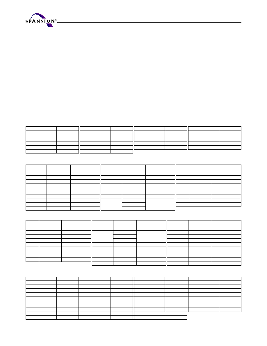
32
S71GL032A Based MCPs
S71GL032A_00_A0 March 31, 2005
A d v a n c e I n f o r m a t i o n
protected sector groups. Sector group protection/unprotection can be imple-
mented via two methods.
Sector protection/unprotection requires V
ID
on the RESET# pin only, and can be
implemented either in-system or via programming equipment.
Figure 2
shows
the algorithms and
Figure 24
shows the timing diagram. This method uses stan-
dard microprocessor bus cycle timing. For sector group unprotect, all unprotected
sector groups must first be protected prior to the first sector group unprotect
write cycle.
The device is shipped with all sector groups unprotected. Spansion offers the op-
tion of programming and protecting sector groups at its factory prior to shipping
the device through Spansion Programming Service. Contact a Spansion represen-
tative for details.
It is possible to determine whether a sector group is protected or unprotected.
See the
Autoselect Mode
section for details.
Table 10. S29GL032A (Models R1, R2) Sector Group Protection/Unprotection Addresses
Sector Group
A20≠A15
Sector Group
A20≠A15
Sector Group
A20≠A15
Sector Group
A20≠A15
SA0
000000
SA12≠SA15
0011xx
SA36≠SA39
1001xx
SA56≠SA59
1110xx
SA1
000001
SA16≠SA19
0100xx
SA40≠SA43
1010xx
SA60
111100
SA2
000010
SA20≠SA23
0101xx
SA44≠SA47
1011xx
SA61
111101
SA3
000011
SA24≠SA27
0110xx
SA48≠SA51
1100xx
SA62
111110
SA4≠SA7
0001xx
SA28≠SA31
0111xx
SA52≠SA55
1101xx
SA63
111111
SA8≠SA11
0010xx
SA32≠SA35
1000xx
Table 11. S29GL032A (Models R3) Sector Group Protection/Unprotection Address Table
Sector
A20≠A12
Sector/Sector
Block Size
(Kbytes)
Sector
A20≠A12
Sector/Sector
Block Size
(Kbytes)
Sector
A20≠A12
Sector/Sector
Block Size
(Kbytes)
SA0-SA3
0000XXXXXh
256 (4x64)
SA36≠SA39
1001XXXXXh
256 (4x64)
SA63
111111000h
8
SA4-SA7
0001XXXXXh
256 (4x64)
SA40≠SA43
1010XXXXXh
256 (4x64)
SA64
111111001h
8
SA8-SA11
0010XXXXXh
256 (4x64)
SA44≠SA47
1011XXXXXh
256 (4x64)
SA65
111111010h
8
SA12-SA15
0011XXXXXh
256 (4x64)
SA48≠SA51
1100XXXXXh
256 (4x64)
SA66
111111011h
8
SA16-SA19
0100XXXXXh
256 (4x64)
SA52-SA55
1101XXXXXh
256 (4x64)
SA67
111111100h
8
SA20-SA23
0101XXXXXh
256 (4x64)
SA56-SA59
1110XXXXXh
256 (4x64)
SA68
111111101h
8
SA24-SA27
0110XXXXXh
256 (4x64)
SA60-SA62
111100XXXh
192 (3x64)
SA69
111111110h
8
SA28-SA31
0111XXXXXh
256 (4x64)
111101XXXh
SA70
111111111h
8
SA32≠SA35
1000XXXXXh
256 (4x64)
111110XXXh
Table 12. S29GL032A (Models R4) Sector Group Protection/Unprotection Address Table
Sector
A20≠A12
Sector/Sector
Block Size
(Kbytes)
Sector
A20≠A12
Sector/Sector
Block Size
(Kbytes)
Sector
A20≠A12
Sector/Sector
Block Size
(Kbytes)
SA0
000000000h
8
SA8≠SA10
000001XXXh
192 (3x64)
SA35-SA38
0111XXXXXh
256 (4x64)
SA1
000000001h
8 000010XXXh
SA39-SA42
1000XXXXXh
256
(4x64)
SA2
000000010h
8 000011XXXh
SA43-SA46
1001XXXXXh
256
(4x64)
SA3
000000011h
8 SA11≠SA14
0001XXXXXh
256
(4x64)
SA47-SA50
1010XXXXXh
256
(4x64)
SA4
000000100h
8 SA15≠SA18
0010XXXXXh
256
(4x64)
SA51-SA54
1011XXXXXh
256
(4x64)
SA5
000000101h
8 SA19≠SA22
0011XXXXXh
256
(4x64)
SA55≠SA58
1100XXXXXh
256
(4x64)
SA6
000000110h
8 SA23≠SA26
0100XXXXXh
256
(4x64)
SA59≠SA62
1101XXXXXh
256
(4x64)
SA7
000000111h
8 SA27-SA30
0101XXXXXh
256
(4x64)
SA63≠SA66
1110XXXXXh
256
(4x64)
SA31-SA34
0110XXXXXh
256 (4x64)
SA67≠SA70
1111XXXXXh
256 (4x64)
Table 13. S29GL064A (Models R1, R2, R8, R9) Sector Group Protection/Unprotection Addresses
Sector Group
A21≠A15
Sector Group
A21≠A15
Sector Group
A21≠A15
Sector Group
A21≠A15
SA0
0000000
SA28≠SA31
00111xx
SA68≠SA71
10001xx
SA108≠SA111
11011xx
SA1
0000001
SA32≠SA35
01000xx
SA72≠SA75
10010xx
SA112≠SA115
11100xx
SA2
0000010
SA36≠SA39
01001xx
SA76≠SA79
10011xx
SA116≠SA119
11101xx
SA3
0000011
SA40≠SA43
01010xx
SA80≠SA83
10100xx
SA120≠SA123
11110xx
SA4≠SA7
00001xx
SA44≠SA47
01011xx
SA84≠SA87
10101xx
SA124
1111100
SA8≠SA11
00010xx
SA48≠SA51
01100xx
SA88≠SA91
10110xx
SA125
1111101
SA12≠SA15
00011xx
SA52≠SA55
01101xx
SA92≠SA95
10111xx
SA126
1111110
SA16≠SA19
00100xx
SA56≠SA59
01110xx
SA96≠SA99
11000xx
SA127
1111111
SA20≠SA23
00101xx
SA60≠SA63
01111xx
SA100≠SA103
11001xx
SA24≠SA27
00110xx
SA64≠SA67
10000xx
SA104≠SA107
11010xx

March 31, 2005 S71GL032A_00_A0
S71GL032A Based MCPs
33
A d v a n c e I n f o r m a t i o n
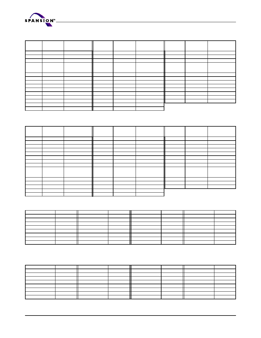
34
S71GL032A Based MCPs
S71GL032A_00_A0 March 31, 2005
A d v a n c e I n f o r m a t i o n
Note:
All sector groups are 128 Kwords in size.
Note:
All sector groups are 128 Kwords in size.
Table 14. S29GL064A (Model R3) Top Boot Sector Protection/Unprotection Addresses
Sector
A21≠A12
Sector/Sector
Block Size
(Kbytes)
Sector
A20≠A12
Sector/Sector
Block Size
(Kbytes)
Sector
A20≠A12
Sector/Sector
Block Size
(Kbytes)
SA0-SA3
00000XXXXX
256 (4x64)
SA56-SA59
01110XXXXX
256 (4x64)
SA112-SA115
11100XXXXX
256 (4x64)
SA4-SA7
00001XXXXX
256 (4x64)
SA60-SA63
01111XXXXX
256 (4x64)
SA116-SA119
11101XXXXX
256 (4x64)
SA8-SA11
00010XXXXX
256 (4x64)
SA64-SA67
10000XXXXX
256 (4x64)
SA120-SA123
11110XXXXX
256 (4x64)
SA12-SA15
00011XXXXX
256 (4x64)
SA68-SA71
10001XXXXX
256 (4x64)
SA124-SA126
1111100XXX
1111101XXX
1111110XXX
192 (3x64)
SA16-SA19
00100XXXXX
256 (4x64)
SA72-SA75
10010XXXXX
256 (4x64)
SA127
1111111000
8
SA20-SA23
00101XXXXX
256 (4x64)
SA76-SA79
10011XXXXX
256 (4x64)
SA128
1111111001
8
SA24-SA27
00110XXXXX
256 (4x64)
SA80-SA83
10100XXXXX
256 (4x64)
SA129
1111111010
8
SA28-SA31
00111XXXXX
256 (4x64)
SA84-SA87
10101XXXXX
256 (4x64)
SA130
1111111011
8
SA32-SA35
01000XXXXX
256 (4x64)
SA88-SA91
10110XXXXX
256 (4x64)
SA131
1111111100
8
SA36-SA39
01001XXXXX
256 (4x64)
SA92-SA95
10111XXXXX
256 (4x64)
SA132
1111111101
8
SA40-SA43
01010XXXXX
256 (4x64)
SA96-SA99
11000XXXXX
256 (4x64)
SA133
1111111110
8
SA44-SA47
01011XXXXX
256 (4x64)
SA100-SA103
11001XXXXX
256 (4x64)
SA134
1111111111
8
SA48-SA51
01100XXXXX
256 (4x64)
SA104-SA107
11010XXXXX
256 (4x64)
SA52-SA55
01101XXXXX
256 (4x64)
SA108-SA111
11011XXXXX
256 (4x64)
Table 15. S29GL064A (Model R4) Bottom Boot Sector Protection/Unprotection Addresses
Sector
A21≠A12
Sector/Sector
Block Size
(Kbytes)
Sector
A20≠A12
Sector/Sector
Block Size
(Kbytes)
Sector
A20≠A12
Sector/Sector
Block Size
(Kbytes)
SA0
0000000000
8
SA31-SA34
00110XXXXX
256 (4x64)
SA87≠SA90
10100XXXXX
256 (4x64)
SA1
0000000001
8
SA35-SA38
00111XXXXX
256 (4x64)
SA91≠SA94
10101XXXXX
256 (4x64)
SA2
0000000010
8
SA39-SA42
01000XXXXX
256 (4x64)
SA95≠SA98
10110XXXXX
256 (4x64)
SA3
0000000011
8
SA43-SA46
01001XXXXX
256 (4x64)
SA99≠SA102
10111XXXXX
256 (4x64)
SA4
0000000100
8
SA47-SA50
01010XXXXX
256 (4x64)
SA103≠SA106
11000XXXXX
256 (4x64)
SA5
0000000101
8
SA51-SA54
01011XXXXX
256 (4x64)
SA107≠SA110
11001XXXXX
256 (4x64)
SA6
0000000110
8
SA55≠SA58
01100XXXXX
256 (4x64)
SA111≠SA114
11010XXXXX
256 (4x64)
SA7
0000000111
8
SA59≠SA62
01101XXXXX
256 (4x64)
SA115≠SA118
11011XXXXX
256 (4x64)
SA8≠SA10
0000001XXX,
0000010XXX,
0000011XXX,
192 (3x64)
SA63≠SA66
01110XXXXX
256 (4x64)
SA119≠SA122
11100XXXXX
256 (4x64)
SA11≠SA14 00001XXXXX
256 (4x64)
SA67≠SA70
01111XXXXX
256 (4x64)
SA123≠SA126
11101XXXXX
256 (4x64)
SA15≠SA18 00010XXXXX
256 (4x64)
SA71≠SA74
10000XXXXX
256 (4x64)
SA127≠SA130
11110XXXXX
256 (4x64)
SA19≠SA22 00011XXXXX
256 (4x64)
SA75≠SA78
10001XXXXX
256 (4x64)
SA131≠SA134
11111XXXXX
256 (4x64)
SA23≠SA26 00100XXXXX
256 (4x64)
SA79≠SA82
10010XXXXX
256 (4x64)
SA27-SA30
00101XXXXX
256 (4x64)
SA83≠SA86
10011XXXXX
256 (4x64)
Table 16. S29GL064A (Model R5) Sector Group Protection/Unprotection Addresses
Sector Group
A21≠A15
Sector Group
A21≠A15
Sector Group
A21≠A15
Sector Group
A21≠A15
SA0≠SA3
00000
SA32≠SA35
01000
SA64≠SA67
10000
SA96≠SA99
11000
SA4≠SA7
00001
SA36≠SA39
01001
SA68≠SA71
10001
SA100≠SA103
11001
SA8≠SA11
00010
SA40≠SA43
01010
SA72≠SA75
10010
SA104≠SA107
11010
SA12≠SA15
00011
SA44≠SA47
01011
SA76≠SA79
10011
SA108≠SA111
11011
SA16≠SA19
00100
SA48≠SA51
01100
SA80≠SA83
10100
SA112≠SA115
11100
SA20≠SA23
00101
SA52≠SA55
01101
SA84≠SA87
10101
SA116≠SA119
11101
SA24≠SA27
00110
SA56≠SA59
01110
SA88≠SA91
10110
SA120≠SA123
11110
SA28≠SA31
00111
SA60≠SA63
01111
SA92≠SA95
10111
SA124≠SA127
11111
Table 17. S29GL064A (Models R6, R7) Sector Group Protection/Unprotection Addresses
Sector Group
A21≠A15
Sector Group
A21≠A15
Sector Group
A21≠A15
Sector Group
A21≠A15
SA0≠SA3
00000
SA32≠SA35
01000
SA64≠SA67
10000
SA96≠SA99
11000
SA4≠SA7
00001
SA36≠SA39
01001
SA68≠SA71
10001
SA100≠SA103
11001
SA8≠SA11
00010
SA40≠SA43
01010
SA72≠SA75
10010
SA104≠SA107
11010
SA12≠SA15
00011
SA44≠SA47
01011
SA76≠SA79
10011
SA108≠SA111
11011
SA16≠SA19
00100
SA48≠SA51
01100
SA80≠SA83
10100
SA112≠SA115
11100
SA20≠SA23
00101
SA52≠SA55
01101
SA84≠SA87
10101
SA116≠SA119
11101
SA24≠SA27
00110
SA56≠SA59
01110
SA88≠SA91
10110
SA120≠SA123
11110
SA28≠SA31
00111
SA60≠SA63
01111
SA92≠SA95
10111
SA124≠SA127
11111
March 31, 2005 S71GL032A_00_A0
S71GL032A Based MCPs
35
A d v a n c e I n f o r m a t i o n
Temporary Sector Group Unprotect
This feature allows temporary unprotection of previously protected sector groups
to change data in-system. The Sector Group Unprotect mode is activated by set-
ting the RESET# pin to V
ID
. During this mode, formerly protected sector groups
can be programmed or erased by selecting the sector group addresses. Once V
ID
is removed from the RESET# pin, all the previously protected sector groups are
protected again.
Figure 1
shows the algorithm, and
Figure 22
shows the timing
diagrams, for this feature.
Notes:
1. All protected sector groups unprotected (If WP# = V
IL
, the highest or lowest address sector will remain protected for
uniform sector devices; the top or bottom two address sectors will remain protected for boot sector devices).
2. All previously protected sector groups are protected once again.
Figure 1. Temporary Sector Group Unprotect Operation
START
Perform Erase or
Program Operations
RESET# = V
IH
Temporary Sector
Group Unprotect Completed
(Note 2)
RESET# = V
ID
(Note 1)
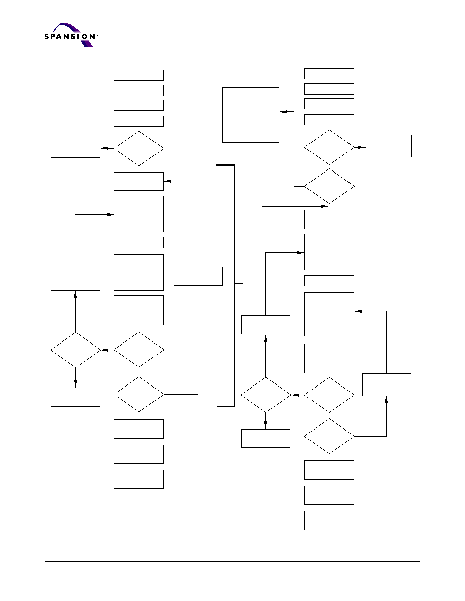
36
S71GL032A Based MCPs
S71GL032A_00_A0 March 31, 2005
A d v a n c e I n f o r m a t i o n
Figure 2. In-System Sector Group Protect/Unprotect Algorithms
Sector Group Protect:
Write 60h to sector
group address with
A6≠A0 = 0xx0010
Set up sector
group address
Wait 150 µs
Verify Sector Group
Protect: Write 40h
to sector group
address with
A6≠A0 = 0xx0010
Read from
sector group address
with A6≠A0
= 0xx0010
START
PLSCNT = 1
RESET# = V
ID
Wait 1
µs
First Write
Cycle = 60h?
Data = 01h?
Remove V
ID
from RESET#
Write reset
command
Sector Group
Protect complete
Yes
Yes
No
PLSCNT
= 25?
Yes
Device failed
Increment
PLSCNT
Temporary Sector
Group Unprotect
Mode
No
Sector Group
Unprotect:
Write 60h to sector
group address with
A6≠A0 = 1xx0010
Set up first sector
group address
Wait 15 ms
Verify Sector Group
Unprotect: Write
40h to sector group
address with
A6≠A0 = 1xx0010
Read from
sector group
address with
A6≠A0 = 1xx0010
START
PLSCNT = 1
RESET# = V
ID
Wait 1
µs
Data = 00h?
Last sector
group
verified?
Remove V
ID
from RESET#
Write reset
command
Sector Group
Unprotect complete
Yes
No
PLSCNT
= 1000?
Yes
Device failed
Increment
PLSCNT
Temporary Sector
Group Unprotect
Mode
No
All sector
groups
protected?
Yes
Protect all sector
groups: The indicated
portion of the sector
group protect algorithm
must be performed for all
unprotected sector
groups prior to issuing
the first sector group
unprotect address
Set up
next sector group
address
No
Yes
No
Yes
No
No
Yes
No
Sector Group
Protect
Algorithm
Sector Group
Unprotect
Algorithm
First Write
Cycle = 60h?
Protect
another
sector group?
Reset
PLSCNT = 1
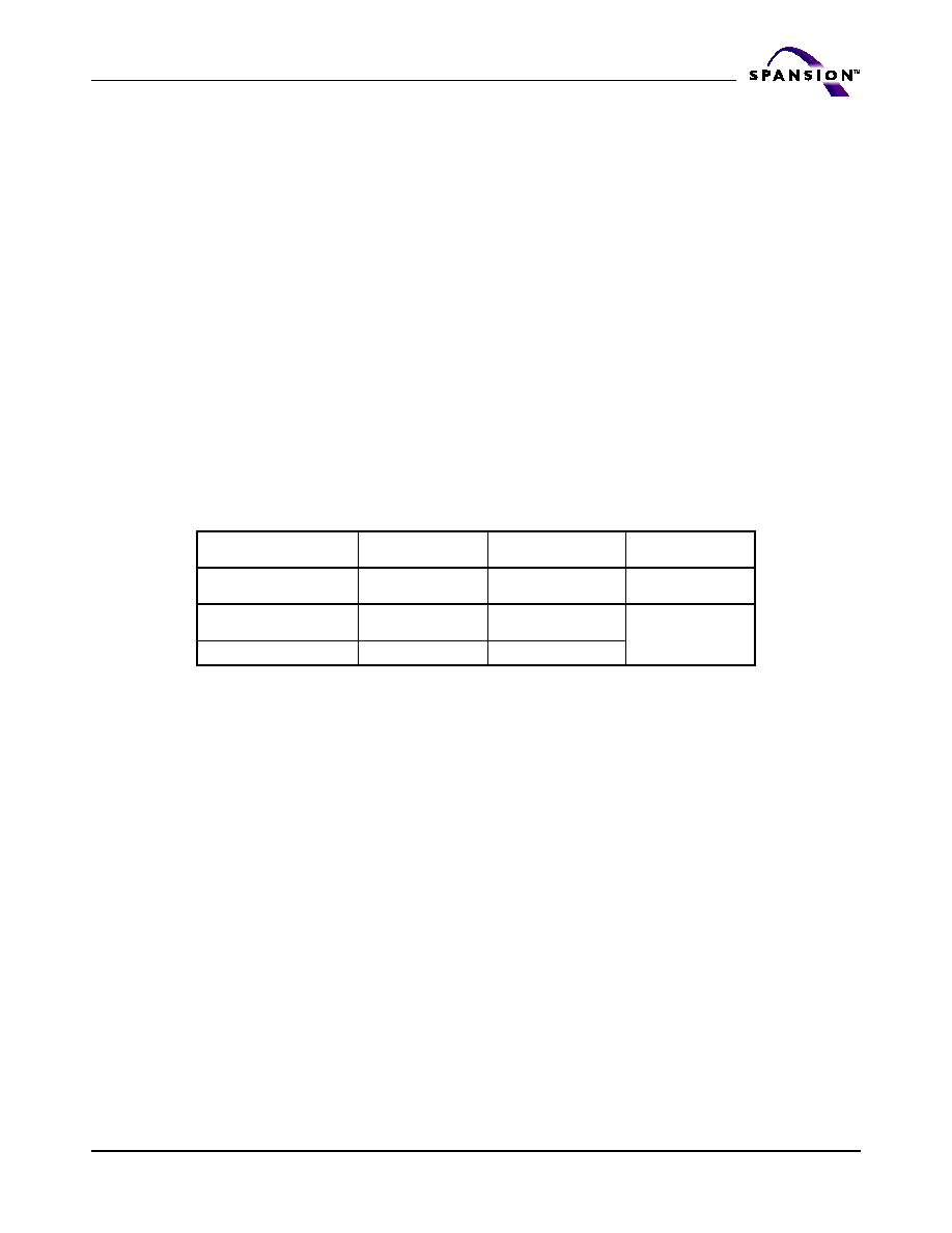
March 31, 2005 S71GL032A_00_A0
S71GL032A Based MCPs
37
A d v a n c e I n f o r m a t i o n
Secured Silicon Sector Flash Memory Region
The Secured Silicon Sector feature provides a Flash memory region that enables
permanent part identification through an Electronic Serial Number (ESN). The
Secured Silicon Sector is 256 bytes in length, and uses a Secured Silicon Sector
Indicator Bit (DQ7) to indicate whether or not the Secured Silicon Sector is locked
when shipped from the factory. This bit is permanently set at the factory and can-
not be changed, which prevents cloning of a factory locked part. This ensures the
security of the ESN once the product is shipped to the field.
The factory offers the device with the Secured Silicon Sector either customer
lockable (standard shipping option) or factory locked (contact a Spansion sales
representative for ordering information). The customer-lockable version is
shipped with the Secured Silicon Sector unprotected, allowing customers to pro-
gram the sector after receiving the device. The customer-lockable version also
has the Secured Silicon Sector Indicator Bit permanently set to a "0." The factory-
locked version is always protected when shipped from the factory, and has the
Secured Silicon Sector Indicator Bit permanently set to a "1." Thus, the Secured
Silicon Sector Indicator Bit prevents customer-lockable devices from being used
to replace devices that are factory locked. Note that the ACC function and unlock
bypass modes are not available when the Secured Silicon Sector is enabled.
The Secured Silicon sector address space in this device is allocated as follows:
The system accesses the Secured Silicon Sector through a command sequence
(see "Write Protect (WP#)"). After the system has written the Enter Secured Sil-
icon Sector command sequence, it may read the Secured Silicon Sector by using
the addresses normally occupied by the first sector (SA0). This mode of operation
continues until the system issues the Exit Secured Silicon Sector command se-
quence, or until power is removed from the device. On power-up, or following a
hardware reset, the device reverts to sending commands to sector SA0.
Customer Lockable: Secured Silicon Sector NOT Programmed or
Protected At the Factory
Unless otherwise specified, the device is shipped such that the customer may
program and protect the 256-byte Secured Silicon sector.
The system may program the Secured Silicon Sector using the write-buffer, ac-
celerated and/or unlock bypass methods, in addition to the standard
programming command sequence. See "Command Definitions" .
Programming and protecting the Secured Silicon Sector must be used with cau-
tion since, once protected, there is no procedure available for unprotecting the
Secured Silicon Sector area and none of the bits in the Secured Silicon Sector
memory space can be modified in any way.
The Secured Silicon Sector area can be protected using one of the following
procedures:
Secured Silicon Sector
Address Range
x16
Standard Factory
Locked
ExpressFlash Factory
Locked
Customer Lockable
000000h≠000007h
ESN
ESN or determined by
customer
Determined by customer
000008h≠00007Fh
Unavailable
Determined by customer

38
S71GL032A Based MCPs
S71GL032A_00_A0 March 31, 2005
A d v a n c e I n f o r m a t i o n
Write the three-cycle Enter Secured Silicon Sector Region command se-
quence, and then follow the in-system sector protect algorithm as shown in
Figure 2
, except that RESET# may be at either V
IH
or V
ID
. This allows in-sys-
tem protection of the Secured Silicon Sector without raising any device pin to
a high voltage. Note that this method is only applicable to the Secured Silicon
Sector.
Write the three-cycle Enter Secured Silicon Sector Region command se-
quence, and then use the alternate method of sector protection described in
the "Sector Group Protection and Unprotection" section.
Once the Secured Silicon Sector is programmed, locked and verified, the system
must write the Exit Secured Silicon Sector Region command sequence to return
to reading and writing within the remainder of the array.
Factory Locked: Secured Silicon Sector Programmed and
Protected At the Factory
In devices with an ESN, the Secured Silicon Sector is protected when the device
is shipped from the factory. The Secured Silicon Sector cannot be modified in any
way. An ESN Factory Locked device has an 16-byte random ESN at addresses
000000h≠000007h. Please contact your sales representative for details on order-
ing ESN Factory Locked devices.
Customers may opt to have their code programmed by the factory through the
Spansion programming service (Customer Factory Locked). The devices are then
shipped from the factory with the Secured Silicon Sector permanently locked.
Contact your sales representative for details on using the Spansion programming
service.
Write Protect (WP#)
The Write Protect function provides a hardware method of protecting the first or
last sector group without using V
ID
. Write Protect is one of two functions provided
by the WP#/ACC input.
If the system asserts V
IL
on the WP#/ACC pin, the device disables program and
erase functions in the first or last sector group independently of whether those
sector groups were protected or unprotected. Note that if WP#/ACC is at V
IL
when the device is in the standby mode, the maximum input load current is in-
creased. See the table in
"DC Characteristics" section on page 65
.
If the system asserts V
IH
on the WP#/ACC pin, the device reverts to
whether the first or last sector was previously set to be protected or un-
protected using the method described in "Sector Group Protection and
Unprotection". Note that WP# has an internal pullup; when uncon-
nected, WP# is at V
IH
.
Hardware Data Protection
The command sequence requirement of unlock cycles for programming or erasing
provides data protection against inadvertent writes (refer to
Table 22
for com-
mand definitions). In addition, the following hardware data protection measures
prevent accidental erasure or programming, which might otherwise be caused by
spurious system level signals during V
CC
power-up and power-down transitions,
or from system noise.

March 31, 2005 S71GL032A_00_A0
S71GL032A Based MCPs
39
A d v a n c e I n f o r m a t i o n
Low V
CC
Write Inhibit
When V
CC
is less than V
LKO
, the device does not accept any write cycles. This pro-
tects data during V
CC
power-up and power-down. The command register and all
internal program/erase circuits are disabled, and the device resets to the read
mode. Subsequent writes are ignored until V
CC
is greater than V
LKO
. The system
must provide the proper signals to the control pins to prevent unintentional writes
when V
CC
is greater than V
LKO
.
Write Pulse "Glitch" Protection
Noise pulses of less than 3 ns (typical) on OE#, CE# or WE# do not initiate a write
cycle.
Logical Inhibit
Write cycles are inhibited by holding any one of OE# = V
IL
, CE# = V
IH
or WE# =
V
IH
. To initiate a write cycle, CE# and WE# must be a logical zero while OE# is a
logical one.
Power-Up Write Inhibit
If WE# = CE# = V
IL
and OE# = V
IH
during power up, the device does not accept
commands on the rising edge of WE#. The internal state machine is automatically
reset to the read mode on power-up.
40
S71GL032A Based MCPs
S71GL032A_00_A0 March 31, 2005
A d v a n c e I n f o r m a t i o n
Common Flash Memory Interface (CFI)
The Common Flash Interface (CFI) specification outlines device and host system
software interrogation handshake, which allows specific vendor-specified soft-
ware algorithms to be used for entire families of devices. Software support can
then be device-independent, JEDEC ID-independent, and forward- and back-
ward-compatible for the specified flash device families. Flash vendors can
standardize their existing interfaces for long-term compatibility.
This device enters the CFI Query mode when the system writes the CFI Query
command, 98h, to address 55h, any time the device is ready to read array data.
The system can read CFI information at the addresses given in
Table 18
-
Table 21
.
To terminate reading CFI data, the system must write the reset command.
The system can also write the CFI query command when the device is in the au-
toselect mode. The device enters the CFI query mode, and the system can read
CFI data at the addresses given in
Table 18
-
Table 21
. The system must write the
reset command to return the device to reading array data.
For further information, please refer to the CFI Specification and CFI Publication
100. Alternatively, contact your sales representative for copies of these
documents.
Table 18. CFI Query Identification String
Addresses
(x16)
Data
Description
10h
11h
12h
0051h
0052h
0059h
Query Unique ASCII string "QRY"
13h
14h
0002h
0000h
Primary OEM Command Set
15h
16h
0040h
0000h
Address for Primary Extended Table
17h
18h
0000h
0000h
Alternate OEM Command Set (00h = none exists)
19h
1Ah
0000h
0000h
Address for Alternate OEM Extended Table (00h = none exists)
March 31, 2005 S71GL032A_00_A0
S71GL032A Based MCPs
41
A d v a n c e I n f o r m a t i o n
Table 19. System Interface String
Note: CFI data related to V
CC
and time-outs may differ from actual V
CC
and time-outs of the product. Please consult the Ordering
Information tables to obtain the V
CC
range for particular part numbers. Please consult the Erase and Programming Performance table
for typical timeout specifications.
Addresses
(x16)
Data
Description
1Bh
0027h
V
CC
Min. (write/erase)
D7≠D4: volt, D3≠D0: 100 millivolt
1Ch
0036h
V
CC
Max. (write/erase)
D7≠D4: volt, D3≠D0: 100 millivolt
1Dh
0000h
V
PP
Min. voltage (00h = no V
PP
pin present)
1Eh
0000h
V
PP
Max. voltage (00h = no V
PP
pin present)
1Fh
0007h
Reserved for future use
20h
0007h
Typical timeout for Min. size buffer write 2
N
µ
s (00h = not supported)
21h
000Ah
Typical timeout per individual block erase 2
N
ms
22h
0000h
Typical timeout for full chip erase 2
N
ms (00h = not supported)
23h
0001h
Reserved for future use
24h
0005h
Max. timeout for buffer write 2
N
times typical
25h
0004h
Max. timeout per individual block erase 2
N
times typical
26h
0000h
Max. timeout for full chip erase 2
N
times typical (00h = not supported)
42
S71GL032A Based MCPs
S71GL032A_00_A0 March 31, 2005
A d v a n c e I n f o r m a t i o n
Table 20. Device Geometry Definition
Addresses
(x16)
Data
Description
27h
00xxh
Device Size = 2
N
byte
0017h = 64 Mb, 0016h = 32Mb
28h
29h
000xh
0000h
Flash Device Interface description (refer to CFI publication 100)
0000h = x8-only bus devices
0001h = x16-only bus devices
0002h = x8/x16 bus devices
2Ah
2Bh
0005h
0000h
Max. number of byte in multi-byte write = 2
N
(00h = not supported)
2Ch
00xxh
Number of Erase Block Regions within device (01h = uniform device,
02h = boot device)
2Dh
2Eh
2Fh
30h
00xxh
000xh
00x0h
000xh
Erase Block Region 1 Information
(refer to the CFI specification or CFI publication 100)
007Fh, 0000h, 0020h, 0000h = 32 Mb (-R1, -R2)
003Fh, 0000h, 0001h = 32 Mb (-R3, R4)
007Fh, 0000h, 0020h, 0000h = 64 Mb (-R1, -R2, -R8, -R9)
007Fh, 0000h, 0000h, 0001h = 64 Mb (-R3, -R4, -R5, -R6, -R7)
31h
32h
33h
34h
00xxh
0000h
0000h
000xh
Erase Block Region 2 Information (refer to CFI publication 100)
003Eh, 0000h, 0000h, 0001h = 32 Mb (-R1, -R2)
007Eh, 0000h, 0000h, 0001h = 64 Mb (-R1, -R2, -R8, -R9)
0000h, 0000h, 0000h, 0000h = all others
35h
36h
37h
38h
0000h
0000h
0000h
0000h
Erase Block Region 3 Information (refer to CFI publication 100)
39h
3Ah
3Bh
3Ch
0000h
0000h
0000h
0000h
Erase Block Region 4 Information (refer to CFI publication 100)
March 31, 2005 S71GL032A_00_A0
S71GL032A Based MCPs
43
A d v a n c e I n f o r m a t i o n
Table 21. Primary Vendor-Specific Extended Query
Addresses
(x16)
Data
Description
40h
41h
42h
0050h
0052h
0049h
Query-unique ASCII string "PRI"
43h
0031h
Major version number, ASCII
44h
0033h
Minor version number, ASCII
45h
000xh
Address Sensitive Unlock (Bits 1-0)
0 = Required, 1 = Not Required
Process Technology (Bits 7-2) 0010b = 200 nm MirrorBit
0009h = x8-only bus devices
0008h = all other devices
46h
0002h
Erase Suspend
0 = Not Supported, 1 = To Read Only, 2 = To Read & Write
47h
0001h
Sector Protect
0 = Not Supported, X = Number of sectors in per group
48h
0001h
Sector Temporary Unprotect
00 = Not Supported, 01 = Supported
49h
0004h
Sector Protect/Unprotect scheme
0004h = Standard Mode (Refer to Text)
4Ah
0000h
Simultaneous Operation
00 = Not Supported, X = Number of Sectors in Bank
4Bh
0000h
Burst Mode Type
00 = Not Supported, 01 = Supported
4Ch
0001h
Page Mode Type
00 = Not Supported, 01 = 4 Word Page, 02 = 8 Word Page
4Dh
00B5h
ACC (Acceleration) Supply Minimum
00h = Not Supported, D7-D4: Volt, D3-D0: 100 mV
4Eh
00C5h
ACC (Acceleration) Supply Maximum
00h = Not Supported, D7-D4: Volt, D3-D0: 100 mV
4Fh
00xxh
Top/Bottom Boot Sector Flag
02h = Bottom Boot Device, 03h = Top Boot Device, 04h = Uniform
sectors bottom WP# protect, 05h = Uniform sectors top WP# protect
50h
0001h
Program Suspend
00h = Not Supported, 01h = Supported

44
S71GL032A Based MCPs
S71GL032A_00_A0 March 31, 2005
A d v a n c e I n f o r m a t i o n
Command Definitions
Writing specific address and data commands or sequences into the command
register initiates device operations.
Table 22
defines the valid register command
sequences. Writing incorrect address and data values or writing them in the im-
proper sequence may place the device in an unknown state. A reset command is
then required to return the device to reading array data.
All addresses are latched on the falling edge of WE# or CE#, whichever happens
later. All data is latched on the rising edge of WE# or CE#, whichever happens
first. Refer to the AC Characteristics section for timing diagrams.
Reading Array Data
The device is automatically set to reading array data after device power-up. No
commands are required to retrieve data. The device is ready to read array data
after completing an Embedded Program or Embedded Erase algorithm.
After the device accepts an Erase Suspend command, the device enters the
erase-suspend-read mode, after which the system can read data from any non-
erase-suspended sector. After completing a programming operation in the Erase
Suspend mode, the system may once again read array data with the same ex-
ception. See the Erase Suspend/Erase Resume Commands section for more
information.
The system must issue the reset command to return the device to the read (or
erase-suspend-read) mode if DQ5 goes high during an active program or erase
operation, or if the device is in the autoselect mode. See the next section, Reset
Command, for more information.
See also Requirements for Reading Array Data in the Device Bus Operations sec-
tion for more information. The Read-Only Operations≠
"AC Characteristics"
section on page 67
provides the read parameters, and
Figure 13
shows the timing
diagram.
Reset Command
Writing the reset command resets the device to the read or erase-suspend-read
mode. Address bits are don't cares for this command.
The reset command may be written between the sequence cycles in an erase
command sequence before erasing begins. This resets the device to the read
mode. Once erasure begins, however, the device ignores reset commands until
the operation is complete.
The reset command may be written between the sequence cycles in a program
command sequence before programming begins. This resets the device to the
read mode. If the program command sequence is written while the device is in
the Erase Suspend mode, writing the reset command returns the device to the
erase-suspend-read mode. Once programming begins, however, the device ig-
nores reset commands until the operation is complete.
The reset command may be written between the sequence cycles in an autoselect
command sequence. Once in the autoselect mode, the reset command must be
written to return to the read mode. If the device entered the autoselect mode
while in the Erase Suspend mode, writing the reset command returns the device
to the erase-suspend-read mode.
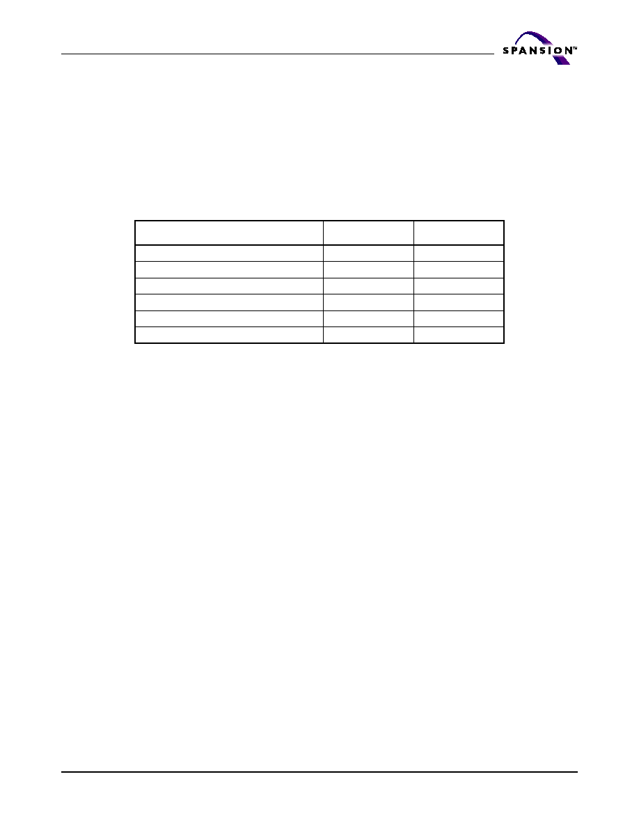
March 31, 2005 S71GL032A_00_A0
S71GL032A Based MCPs
45
A d v a n c e I n f o r m a t i o n
If DQ5 goes high during a program or erase operation, writing the reset command
returns the device to the read mode (or erase-suspend-read mode if the device
was in Erase Suspend).
Note that if DQ1 goes high during a Write Buffer Programming operation, the sys-
tem must write the Write-to-Buffer-Abort Reset command sequence to reset the
device for the next operation.
Autoselect Command Sequence
The autoselect command sequence allows the host system to read several iden-
tifier codes at specific addresses:
Note: The device ID is read over three cycles. SA = Sector Address
The autoselect command sequence is initiated by first writing two unlock cycles.
This is followed by a third write cycle that contains the autoselect command. The
device then enters the autoselect mode. The system may read at any address any
number of times without initiating another autoselect command sequence:
The system must write the reset command to return to the read mode (or erase-
suspend-read mode if the device was previously in Erase Suspend).
Enter Secured Silicon Sector/Exit Secured Silicon
Sector Command Sequence
The Secured Silicon Sector region provides a secured data area containing an 8-
word random Electronic Serial Number (ESN). The system can access the Se-
cured Silicon Sector region by issuing the three-cycle Enter Secured Silicon
Sector command sequence. The device continues to access the Secured Silicon
Sector region until the system issues the four-cycle Exit Secured Silicon Sector
command sequence. The Exit Secured Silicon Sector command sequence returns
the device to normal operation.
Table 22
shows the address and data require-
ments for both command sequences. See also "Secured Silicon Sector Flash
Memory Region" for further information. Note that the ACC function and unlock
bypass modes are not available when the Secured Silicon Sector is enabled.
Word Program Command Sequence
Programming is a four-bus-cycle operation. The program command sequence is
initiated by writing two unlock write cycles, followed by the program set-up com-
mand. The program address and data are written next, which in turn initiate the
Embedded Program algorithm. The system is not required to provide further con-
trols or timings. The device automatically provides internally generated program
pulses and verifies the programmed cell margin.
Table 22
shows the address and
data requirements for the word program command sequence, respectively.
Identifier Code
A7:A0
(x16)
A6:A-1
(x8)
Manufacturer ID
00h
00h
Device ID, Cycle 1
01h
02h
Device ID, Cycle 2
0Eh
1Ch
Device ID, Cycle 3
0Fh
1Eh
Secured Silicon Sector Factory Protect
03h
06h
Sector Protect Verify
(SA)02h
(SA)04h

46
S71GL032A Based MCPs
S71GL032A_00_A0 March 31, 2005
A d v a n c e I n f o r m a t i o n
When the Embedded Program algorithm is complete, the device then returns to
the read mode and addresses are no longer latched. The system can determine
the status of the program operation by using DQ7 or DQ6. Refer to the Write Op-
eration Status section for information on these status bits. Any commands
written to the device during the Embedded Program Algorithm are ignored. Note
that the Secured Silicon Sector, autoselect, and CFI functions are unavailable
when a program operation is in progress. Note that a hardware reset immedi-
ately terminates the program operation. The program command sequence should
be reinitiated once the device has returned to the read mode, to ensure data
integrity.
Programming is allowed in any sequence of address locations and across sector
boundaries. Programming to the same word address multiple times without in-
tervening erases (incremental bit programming) requires a modified
programming method. For such application requirements, please contact your
local Spansion representative. Word programming is supported for backward
compatibility with existing Flash driver software and for occasional writing of in-
dividual words. Use of write buffer programming (see below) is strongly
recommended for general programming use when more than a few words are to
be programmed. The effective word programming time using write buffer pro-
gramming is approximately four times shorter than the single word programming
time.
Any bit in a word cannot be programmed from "0" back to a "1." Attempt-
ing to do so may cause the device to set DQ5=1, or cause DQ7 and DQ6 status
bits to indicate the operation was successful. However, a succeeding read will
show that the data is still "0." Only erase operations can convert a "0" to a "1."
Unlock Bypass Command Sequence
The unlock bypass feature allows the system to program words to the device
faster than using the standard program command sequence. The unlock bypass
command sequence is initiated by first writing two unlock cycles. This is followed
by a third write cycle containing the unlock bypass command, 20h. The device
then enters the unlock bypass mode. A two-cycle unlock bypass mode command
sequence is all that is required to program in this mode. The first cycle in this se-
quence contains the unlock bypass program command, A0h; the second cycle
contains the program address and data. Additional data is programmed in the
same manner. This mode dispenses with the initial two unlock cycles required in
the standard program command sequence, resulting in faster total programming
time.
Table 22
shows the requirements for the command sequence.
During the unlock bypass mode, only the Unlock Bypass Program and Unlock By-
pass Reset commands are valid. To exit the unlock bypass mode, the system
must issue the two-cycle unlock bypass reset command sequence. The first cycle
must contain the data 90h. The second cycle must contain the data 00h. The de-
vice then returns to the read mode.
Write Buffer Programming
Write Buffer Programming allows the system write to a maximum of 16 in one
programming operation. This results in faster effective programming time than
the standard programming algorithms. The Write Buffer Programming command
sequence is initiated by first writing two unlock cycles. This is followed by a third
write cycle containing the Write Buffer Load command written at the Sector Ad-
dress in which programming will occur. The fourth cycle writes the sector address
and the number of word locations, minus one, to be programmed. For example,

March 31, 2005 S71GL032A_00_A0
S71GL032A Based MCPs
47
A d v a n c e I n f o r m a t i o n
if the system will program 6 unique address locations, then 05h should be written
to the device. This tells the device how many write buffer addresses will be loaded
with data and therefore when to expect the Program Buffer to Flash command.
The number of locations to program cannot exceed the size of the write buffer or
the operation will abort.
The fifth cycle writes the first address location and data to be programmed. The
write-buffer-page is selected by address bits A
MAX
≠A
4
. All subsequent address/
data pairs must fall within the selected-write-buffer-page. The system then
writes the remaining address/data pairs into the write buffer. Write buffer loca-
tions may be loaded in any order.
The write-buffer-page address must be the same for all address/data pairs loaded
into the write buffer. (This means Write Buffer Programming cannot be performed
across multiple write-buffer pages.) This also means that Write Buffer Program-
ming cannot be performed across multiple sectors. If the system attempts to load
programming data outside of the selected write-buffer page, the operation will
abort.
Note that if a Write Buffer address location is loaded multiple times, the address/
data pair counter will be decremented for every data load operation. The host
system must therefore account for loading a write-buffer location more than
once. The counter decrements for each data load operation, not for each unique
write-buffer-address location. Note also that if an address location is loaded more
than once into the buffer, the final data loaded for that address will be
programmed.
Once the specified number of write buffer locations have been loaded, the system
must then write the Program Buffer to Flash command at the sector address. Any
other address and data combination aborts the Write Buffer Programming oper-
ation. The device then begins programming. Data polling should be used while
monitoring the last address location loaded into the write buffer. DQ7, DQ6, DQ5,
and DQ1 should be monitored to determine the device status during Write Buffer
Programming.
The write-buffer programming operation can be suspended using the standard
program suspend/resume commands. Upon successful completion of the Write
Buffer Programming operation, the device is ready to execute the next command.
The Write Buffer Programming Sequence can be aborted in the following ways:
Load a value that is greater than the page buffer size during the Number of
Locations to Program step.
Write to an address in a sector different than the one specified during the
Write-Buffer-Load command.
Write an Address/Data pair to a different write-buffer-page than the one se-
lected by the Starting Address during the write buffer data loading stage of
the operation.
Write data other than the Confirm Command after the specified number of
data load cycles.
The abort condition is indicated by DQ1 = 1, DQ7 = DATA# (for the last address
location loaded), DQ6 = toggle, and DQ5=0. A Write-to-Buffer-Abort Reset com-
mand sequence must be written to reset the device for the next operation.
Note that the Secured Silicon Sector, autoselect, and CFI functions are unavail-
able when a program operation is in progress.This flash device is capable of
handling multiple write buffer programming operations on the same write buffer
address range without intervening erases. For applications requiring incremental

48
S71GL032A Based MCPs
S71GL032A_00_A0 March 31, 2005
A d v a n c e I n f o r m a t i o n
bit programming, a modified programming method is required; please contact
your local Spansion representative. Any bit in a write buffer address range
cannot be programmed from "0" back to a "1." Attempting to do so may
cause the device to set DQ5=1, of cause the DQ7 and DQ6 status bits to indicate
the operation was successful. However, a succeeding read will show that the data
is still "0." Only erase operations can convert a "0" to a "1."
Accelerated Program
The device offers accelerated program operations through the WP#/ACC or ACC
pin depending on the particular product. When the system asserts V
HH
on the
WP#/ACC or ACC pin. The device uses the higher voltage on the WP#/ACC or ACC
pin to accelerate the operation. Note that the WP#/ACC pin must not be at V
HH
for operations other than accelerated programming, or device damage may re-
sult. WP# has an internal pullup; when unconnected, WP# is at V
IH
.
Figure 3
illustrates the algorithm for the program operation. Refer to the Erase
and Program Operations≠
"AC Characteristics" section on page 67
section for pa-
rameters, and
Figure 14
for timing diagrams.
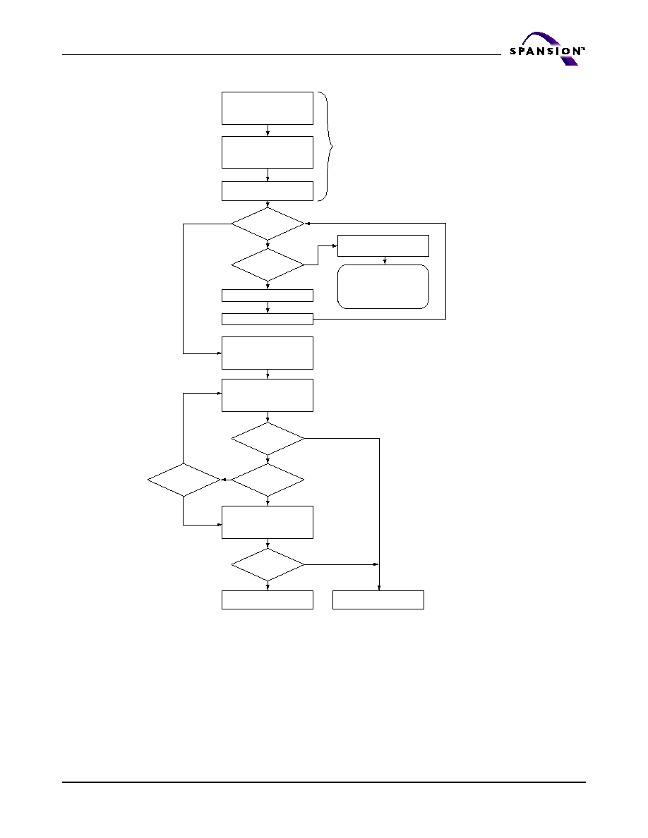
March 31, 2005 S71GL032A_00_A0
S71GL032A Based MCPs
49
A d v a n c e I n f o r m a t i o n
Notes:
1. When Sector Address is specified, any address in the selected sector is acceptable. However, when loading Write-Buffer
address locations with data, all addresses must fall within the selected Write-Buffer Page.
2. DQ7 may change simultaneously with DQ5. Therefore, DQ7 should be verified.
3. If this flowchart location was reached because DQ5= "1", then the device FAILED. If this flowchart location was reached
because DQ1= "1", then the Write to Buffer operation was ABORTED. In either case, the proper reset command must be
written before the device can begin another operation. If DQ1=1, write the Write-Buffer-Programming-Abort-Reset
command. if DQ5=1, write the Reset command.
4. See
Table 22
for command sequences required for write buffer programming.
Figure 3. Write Buffer Programming Operation
Write "Write to Buffer"
command and
Sector Address
Write number of addresses
to program minus 1(WC)
and Sector Address
Write program buffer to
flash sector address
Write first address/data
Write to a different
sector address
FAIL or ABORT
PASS
Read DQ7 - DQ0 at
Last Loaded Address
Read DQ7 - DQ0 with
address = Last Loaded
Address
Write next address/data pair
WC = WC - 1
WC = 0 ?
Part of "Write to Buffer"
Command Sequence
Yes
Yes
Yes
Yes
Yes
Yes
No
No
No
No
No
No
Abort Write to
Buffer Operation?
DQ7 = Data?
DQ7 = Data?
DQ5 = 1?
DQ1 = 1?
Write to buffer ABORTED.
Must write "Write-to-buffer
Abort Reset" command
sequence to return
to read mode.
(Note 2)
(Note 3)
(Note 1)
50
S71GL032A Based MCPs
S71GL032A_00_A0 March 31, 2005
A d v a n c e I n f o r m a t i o n
Note:See
Table 22
for program command sequence.
Figure 4. Program Operation
Program Suspend/Program Resume Command Sequence
The Program Suspend command allows the system to interrupt a programming
operation or a Write to Buffer programming operation so that data can be read
from any non-suspended sector. When the Program Suspend command is written
during a programming process, the device halts the program operation within 15
µs maximum (5µs typical) and updates the status bits. Addresses are not re-
quired when writing the Program Suspend command.
After the programming operation has been suspended, the system can read array
data from any non-suspended sector. The Program Suspend command may also
be issued during a programming operation while an erase is suspended. In this
case, data may be read from any addresses not in Erase Suspend or Program
Suspend. If a read is needed from the Secured Silicon Sector area (One-time Pro-
gram area), then user must use the proper command sequences to enter and exit
this region. Note that the Secured Silicon Sector, autoselect, and CFI functions
are unavailable when a program operation is in progress.
The system may also write the autoselect command sequence when the device
is in the Program Suspend mode. The system can read as many autoselect codes
as required. When the device exits the autoselect mode, the device reverts to the
Program Suspend mode, and is ready for another valid operation. See Autoselect
Command Sequence for more information.
START
Write Program
Command Sequence
Data Poll
from System
Verify Data?
No
Yes
Last Address?
No
Yes
Programming
Completed
Increment Address
Embedded
Program
algorithm
in progress
March 31, 2005 S71GL032A_00_A0
S71GL032A Based MCPs
51
A d v a n c e I n f o r m a t i o n
After the Program Resume command is written, the device reverts to program-
ming. The system can determine the status of the program operation using the
DQ7 or DQ6 status bits, just as in the standard program operation. See Write Op-
eration Status for more information.
The system must write the Program Resume command (address bits are don't
care) to exit the Program Suspend mode and continue the programming opera-
tion. Further writes of the Resume command are ignored. Another Program
Suspend command can be written after the device has resumed programming.
Figure 5. Program Suspend/Program Resume
Chip Erase Command Sequence
Chip erase is a six bus cycle operation. The chip erase command sequence is ini-
tiated by writing two unlock cycles, followed by a set-up command. Two
additional unlock write cycles are then followed by the chip erase command,
which in turn invokes the Embedded Erase algorithm. The device does not require
the system to preprogram prior to erase. The Embedded Erase algorithm auto-
matically preprograms and verifies the entire memory for an all zero data pattern
prior to electrical erase. The system is not required to provide any controls or tim-
ings during these operations.
Table 22
shows the address and data requirements
for the chip erase command sequence.
When the Embedded Erase algorithm is complete, the device returns to the read
mode and addresses are no longer latched. The system can determine the status
of the erase operation by using DQ7, DQ6, or DQ2. Refer to the Write Operation
Status section for information on these status bits.
Program Operation
or Write-to-Buffer
Sequence in Progress
Write Program Suspend
Command Sequence
Command is also valid for
Erase-suspended-program
operations
Autoselect and SecSi Sector
read operations are also allowed
Data cannot be read from erase- or
program-suspended sectors
Write Program Resume
Command Sequence
Read data as
required
Done
reading?
No
Yes
Write address/data
XXXh/30h
Device reverts to
operation prior to
Program Suspend
Write address/data
XXXh/B0h
Wait 15
µs

52
S71GL032A Based MCPs
S71GL032A_00_A0 March 31, 2005
A d v a n c e I n f o r m a t i o n
Any commands written during the chip erase operation are ignored. However,
note that a hardware reset immediately terminates the erase operation. If that
occurs, the chip erase command sequence should be reinitiated once the device
has returned to reading array data, to ensure data integrity.
Figure 6
illustrates the algorithm for the erase operation. Refer to the Erase and
Program Operations table in the AC Characteristics section for parameters, and
Figure 18
section for timing diagrams.

March 31, 2005 S71GL032A_00_A0
S71GL032A Based MCPs
53
A d v a n c e I n f o r m a t i o n
Sector Erase Command Sequence
Sector erase is a six bus cycle operation. The sector erase command sequence is
initiated by writing two unlock cycles, followed by a set-up command. Two addi-
tional unlock cycles are written, and are then followed by the address of the
sector to be erased, and the sector erase command.
Table 22
shows the address
and data requirements for the sector erase command sequence.
The device does not require the system to preprogram prior to erase. The Em-
bedded Erase algorithm automatically programs and verifies the entire memory
for an all zero data pattern prior to electrical erase. The system is not required to
provide any controls or timings during these operations.
After the command sequence is written, a sector erase time-out of 50 µs occurs.
During the time-out period, additional sector addresses and sector erase com-
mands may be written. Loading the sector erase buffer may be done in any
sequence, and the number of sectors may be from one sector to all sectors. The
time between these additional cycles must be less than 50 µs, otherwise erasure
may begin. Any sector erase address and command following the exceeded time-
out may or may not be accepted. It is recommended that processor interrupts be
disabled during this time to ensure all commands are accepted. The interrupts
can be re-enabled after the last Sector Erase command is written. Any com-
mand other than Sector Erase or Erase Suspend during the time-out
period resets the device to the read mode. Note that the Secured Silicon
Sector, autoselect, and CFI functions are unavailable when an erase op-
eration is in progress. The system must rewrite the command sequence and
any additional addresses and commands.
The system can monitor DQ3 to determine if the sector erase timer has timed out
(See the section on DQ3: Sector Erase Timer.). The time-out begins from the ris-
ing edge of the final WE# pulse in the command sequence.
When the Embedded Erase algorithm is complete, the device returns to reading
array data and addresses are no longer latched. The system can determine the
status of the erase operation by reading DQ7, DQ6, or DQ2 in the erasing sector.
Refer to the Write Operation Status section for information on these status bits.
Once the sector erase operation has begun, only the Erase Suspend command is
valid. All other commands are ignored. However, note that a hardware reset im-
mediately terminates the erase operation. If that occurs, the sector erase
command sequence should be reinitiated once the device has returned to reading
array data, to ensure data integrity.
Figure 6
illustrates the algorithm for the erase operation. Refer to the Erase and
Program Operations table in the AC Characteristics section for parameters, and
Figure 18
section for timing diagrams.
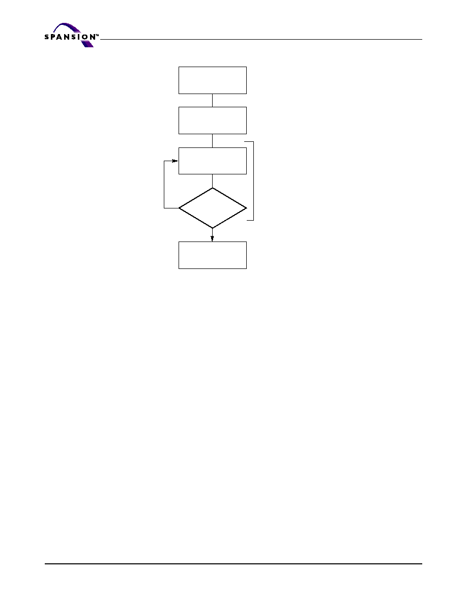
54
S71GL032A Based MCPs
S71GL032A_00_A0 March 31, 2005
A d v a n c e I n f o r m a t i o n
Notes:
1. See
Table 22
for program command sequence.
2. See the section on DQ3 for information on the sector erase timer.
Figure 6. Erase Operation
Erase Suspend/Erase Resume Commands
The Erase Suspend command, B0h, allows the system to interrupt a sector erase
operation and then read data from, or program data to, any sector not selected
for erasure. This command is valid only during the sector erase operation, includ-
ing the 50 µs time-out period during the sector erase command sequence. The
Erase Suspend command is ignored if written during the chip erase operation or
Embedded Program algorithm.
When the Erase Suspend command is written during the sector erase operation,
the device requires a typical of 5 µs
(maximum of 20 µs) to suspend the erase
operation. However, when the Erase Suspend command is written during the sec-
tor erase time-out, the device immediately terminates the time-out period and
suspends the erase operation.
After the erase operation has been suspended, the device enters the erase-sus-
pend-read mode. The system can read data from or program data to any sector
not selected for erasure. (The device "erase suspends" all sectors selected for
erasure.) Reading at any address within erase-suspended sectors produces sta-
tus information on DQ7≠DQ0. The system can use DQ7, or DQ6 and DQ2
together, to determine if a sector is actively erasing or is erase-suspended. Refer
to the Write Operation Status section for information on these status bits.
After an erase-suspended program operation is complete, the device returns to
the erase-suspend-read mode. The system can determine the status of the pro-
gram operation using the DQ7 or DQ6 status bits, just as in the standard word
START
Write Erase
Command Sequence
(Notes 1, 2)
Data Poll to Erasing
Bank from System
Data = FFh?
No
Yes
Erasure Completed
Embedded
Erase
algorithm
in progress

March 31, 2005 S71GL032A_00_A0
S71GL032A Based MCPs
55
A d v a n c e I n f o r m a t i o n
program operation. Refer to the Write Operation Status section for more
information.
In the erase-suspend-read mode, the system can also issue the autoselect com-
mand sequence. Refer to the
"Autoselect Mode" section on page 31
and
"Autoselect Command Sequence" section on page 45
sections for details.
To resume the sector erase operation, the system must write the Erase Resume
command. Further writes of the Resume command are ignored. Another Erase
Suspend command can be written after the chip has resumed erasing.
Note:During an erase operation, this flash device performs multiple internal operations which are invisible to the system. When an
erase operation is suspended, any of the internal operations that were not fully completed must be restarted. As such, if this flash
device is continually issued suspend/resume commands in rapid succession, erase progress will be impeded as a function of the
number of suspends. The result will be a longer cumulative erase time than without suspends. Note that the additional suspends do
not affect device reliability or future performance. In most systems rapid erase/suspend activity occurs only briefly. In such cases,
erase performance will not be significantly impacted.
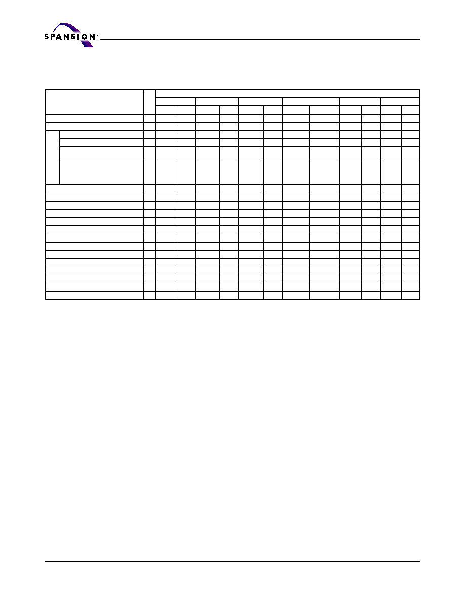
56
S71GL032A Based MCPs
S71GL032A_00_A0 March 31, 2005
A d v a n c e I n f o r m a t i o n
Command Definitions
Table 22. Command Definitions (x16 Mode)
Command
Sequence
(Note 1)
Cy
c
l
es
Bus Cycles (Notes 2≠5)
First
Second
Third
Fourth
Fifth
Sixth
Addr Data
Addr
Data
Addr
Data
Addr
Data
Addr
Data Addr Data
Read (Note 6)
1
RA
RD
Reset (Note 7)
1
XXX
F0
Auto
select (Note
8)
Manufacturer ID
4
555
AA
2AA
55
555
90
X00
0001
Device ID (Note 9)
4
555
AA
2AA
55
555
90
X01
227E
X0E
X0F
Secured Silicon
Sector Factory
Protect (Note 10)
4
555
AA
2AA
55
555
90
X03
(Note 10)
Sector Group Protect Verify (Note
12)
4
555
AA
2AA
55
555
90
(SA)X02
00/01
Enter Secured Silicon Sector Region
3
555
AA
2AA
55
555
88
Exit Secured Silicon Sector Region
4
555
AA
2AA
55
555
90
XXX
00
Program
4
555
AA
2AA
55
555
A0
PA
PD
Write to Buffer (Note 11)
3
555
AA
2AA
55
SA
25
SA
WC
PA
PD
WBL
PD
Program Buffer to Flash
1
SA
29
Write to Buffer Abort Reset (Note 13)
3
555
AA
2AA
55
555
F0
Unlock Bypass
3
555
AA
2AA
55
555
20
Unlock Bypass Program (Note 14)
2
XXX
A0
PA
PD
Unlock Bypass Reset (Note 15)
2
XXX
90
XXX
00
Chip Erase
6
555
AA
2AA
55
555
80
555
AA
2AA
55
555
10
Sector Erase
6
555
AA
2AA
55
555
80
555
AA
2AA
55
SA
30
Program/Erase Suspend (Note 16)
1
XXX
B0
Program/Erase Resume (Note 17)
1
XXX
30
CFI Query (Note 18)
1
55
98
Legend:
X = Don't care
RA = Read Address of memory location to be read.
RD = Read Data read from location RA during read operation.
PA = Program Address. Addresses latch on falling edge of WE# or
CE# pulse, whichever happens later.
PD = Program Data for location PA. Data latches on rising edge of
WE# or CE# pulse, whichever happens first.
SA = Sector Address of sector to be verified (in autoselect mode) or
erased. Address bits A21≠A15 uniquely select any sector.
WBL = Write Buffer Location. Address must be within same write
buffer page as PA.
WC = Word Count. Number of write buffer locations to load minus 1.
Notes:
1. See
Table 1
for description of bus operations.
2. All values are in hexadecimal.
3. Shaded cells indicate read cycles. All others are write cycles.
4. During unlock and command cycles, when lower address bits are
555 or 2AA as shown in table, address bits above A11 and data
bits above DQ7 are don't care.
5. No unlock or command cycles required when device is in read
mode.
6. Reset command is required to return to read mode (or to erase-
suspend-read mode if previously in Erase Suspend) when device
is in autoselect mode, or if DQ5 goes high while device is
providing status information.
7. Fourth cycle of the autoselect command sequence is a read
cycle. Data bits DQ15≠DQ8 are don't care. Except for RD, PD
and WC. See
Autoselect Command Sequence
section for more
information.
8. Device ID must be read in three cycles.
9. If WP# protects highest address sector, data is 98h for factory
locked and 18h for not factory locked. If WP# protects lowest
address sector, data is 88h for factory locked and 08h for not
factor locked.
10. Data is 00h for an unprotected sector group and 01h for a
protected sector group.
11. Total number of cycles in command sequence is determined by
number of words written to write buffer. Maximum number of
cycles in command sequence is 21, including "Program Buffer to
Flash" command.
12. Command sequence resets device for next command after
aborted write-to-buffer operation.
13. Unlock Bypass command is required prior to Unlock Bypass
Program command.
14. Unlock Bypass Reset command is required to return to read
mode when device is in unlock bypass mode.
15. System may read and program in non-erasing sectors, or enter
autoselect mode, when in Erase Suspend mode. Erase Suspend
command is valid only during a sector erase operation.
16. Erase Resume command is valid only during Erase Suspend
mode.
17. Command is valid when device is ready to read array data or
when device is in autoselect mode.

March 31, 2005 S71GL032A_00_A0
S71GL032A Based MCPs
57
A d v a n c e I n f o r m a t i o n
Write Operation Status
The device provides several bits to determine the status of a program or erase
operation: DQ2, DQ3, DQ5, DQ6, and DQ7.
Table 23
and the following subsec-
tions describe the function of these bits. DQ7 and DQ6 each offer a method for
determining whether a program or erase operation is complete or in progress.
The device also provides a hardware-based output signal, RY/BY#, to determine
whether an Embedded Program or Erase operation is in progress or has been
completed.
DQ7: Data# Polling
The Data# Polling bit, DQ7, indicates to the host system whether an Embedded
Program or Erase algorithm is in progress or completed, or whether the device is
in Erase Suspend. Data# Polling is valid after the rising edge of the final WE#
pulse in the command sequence.
During the Embedded Program algorithm, the device outputs on DQ7 the com-
plement of the datum programmed to DQ7. This DQ7 status also applies to
programming during Erase Suspend. When the Embedded Program algorithm is
complete, the device outputs the datum programmed to DQ7. The system must
provide the program address to read valid status information on DQ7. If a pro-
gram address falls within a protected sector, Data# Polling on DQ7 is active for
approximately 1 µs, then the device returns to the read mode.
During the Embedded Erase algorithm, Data# Polling produces a "0" on DQ7.
When the Embedded Erase algorithm is complete, or if the device enters the
Erase Suspend mode, Data# Polling produces a "1" on DQ7. The system must
provide an address within any of the sectors selected for erasure to read valid
status information on DQ7.
After an erase command sequence is written, if all sectors selected for erasing
are protected, Data# Polling on DQ7 is active for approximately 100 µs, then the
device returns to the read mode. If not all selected sectors are protected, the Em-
bedded Erase algorithm erases the unprotected sectors, and ignores the selected
sectors that are protected. However, if the system reads DQ7 at an address within
a protected sector, the status may not be valid.
Just prior to the completion of an Embedded Program or Erase operation, DQ7
may change asynchronously with DQ0≠DQ6 while Output Enable (OE#) is as-
serted low. That is, the device may change from providing status information to
valid data on DQ7. Depending on when the system samples the DQ7 output, it
may read the status or valid data. Even if the device has completed the program
or erase operation and DQ7 has valid data, the data outputs on DQ0≠DQ6 may
be still invalid. Valid data on DQ0≠DQ7 will appear on successive read cycles.
Table 23
shows the outputs for Data# Polling on DQ7.
Figure 7
shows the Data#
Polling algorithm.
Figure 19
in the AC Characteristics section shows the Data#
Polling timing diagram.
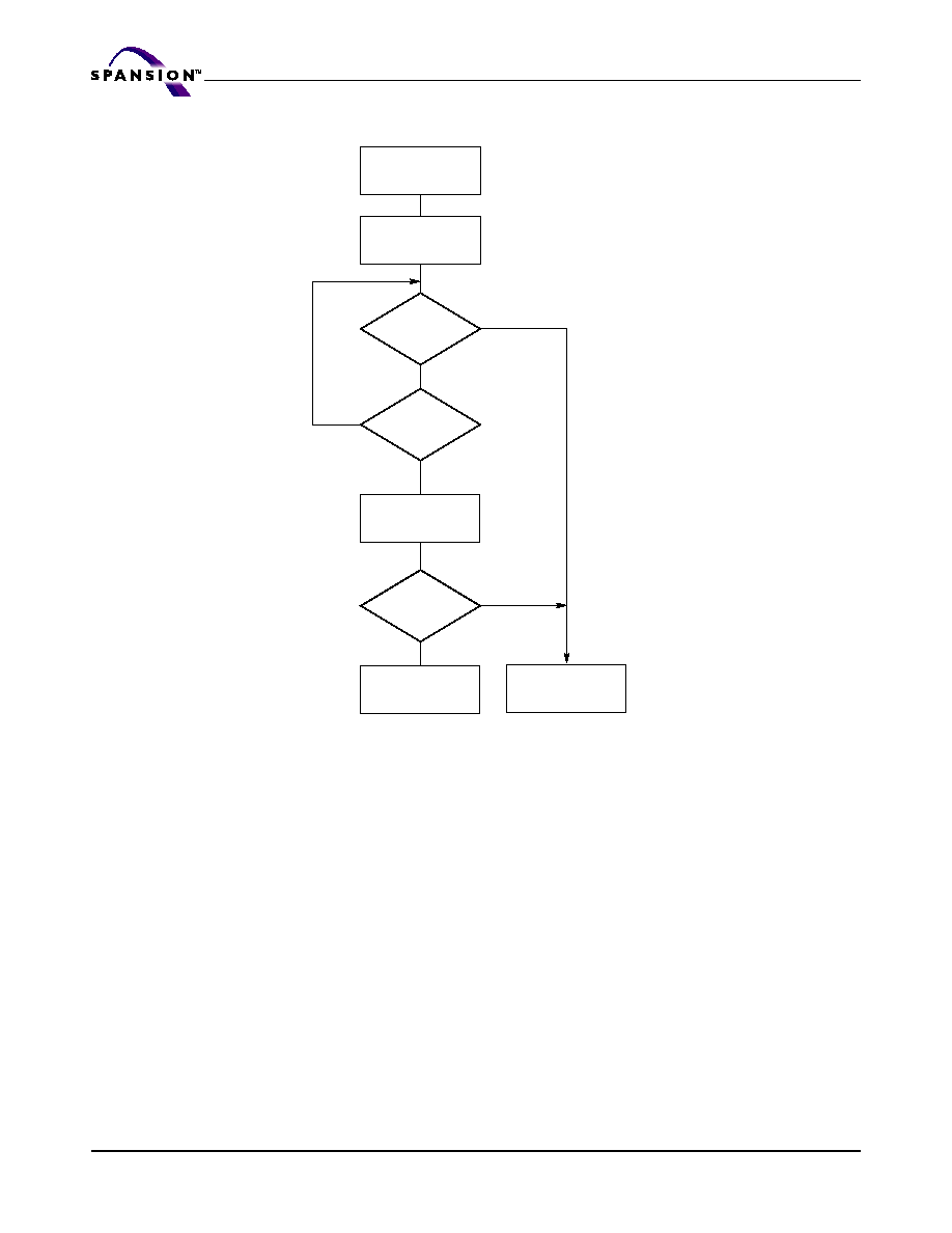
58
S71GL032A Based MCPs
S71GL032A_00_A0 March 31, 2005
A d v a n c e I n f o r m a t i o n
Notes:
1. VA = Valid address for programming. During a sector erase operation, a valid address is any sector address within the sector
being erased. During chip erase, a valid address is any non-protected sector address.
2. DQ7 should be rechecked even if DQ5 = "1" because DQ7 may change simultaneously with DQ5.
Figure 7. Data# Polling Algorithm
RY/BY#: Ready/Busy#
The RY/BY# is a dedicated, open-drain output pin which indicates whether an
Embedded Algorithm is in progress or complete. The RY/BY# status is valid after
the rising edge of the final WE# pulse in the command sequence. Since RY/BY#
is an open-drain output, several RY/BY# pins can be tied together in parallel with
a pull-up resistor to V
CC
.
If the output is low (Busy), the device is actively erasing or programming. (This
includes programming in the Erase Suspend mode.) If the output is high (Ready),
the device is in the read mode, the standby mode, or in the erase-suspend-read
mode.
Table 23
shows the outputs for RY/BY#.
DQ7 = Data?
Yes
No
No
DQ5 = 1?
No
Yes
Yes
FAIL
PASS
Read DQ7≠DQ0
Addr = VA
Read DQ7≠DQ0
Addr = VA
DQ7 = Data?
START

March 31, 2005 S71GL032A_00_A0
S71GL032A Based MCPs
59
A d v a n c e I n f o r m a t i o n
DQ6: Toggle Bit I
Toggle Bit I on DQ6 indicates whether an Embedded Program or Erase algorithm
is in progress or complete, or whether the device has entered the Erase Suspend
mode. Toggle Bit I may be read at any address, and is valid after the rising edge
of the final WE# pulse in the command sequence (prior to the program or erase
operation), and during the sector erase time-out.
During an Embedded Program or Erase algorithm operation, successive read cy-
cles to any address cause DQ6 to toggle. The system may use either OE# or CE#
to control the read cycles. When the operation is complete, DQ6 stops toggling.
After an erase command sequence is written, if all sectors selected for erasing
are protected, DQ6 toggles for approximately 100 µs, then returns to reading
array data. If not all selected sectors are protected, the Embedded Erase algo-
rithm erases the unprotected sectors, and ignores the selected sectors that are
protected.
The system can use DQ6 and DQ2 together to determine whether a sector is ac-
tively erasing or is erase-suspended. When the device is actively erasing (that is,
the Embedded Erase algorithm is in progress), DQ6 toggles. When the device en-
ters the Erase Suspend mode, DQ6 stops toggling. However, the system must
also use DQ2 to determine which sectors are erasing or erase-suspended. Alter-
natively, the system can use DQ7 (see the subsection on DQ7: Data# Polling).
If a program address falls within a protected sector, DQ6 toggles for approxi-
mately 1 µs after the program command sequence is written, then returns to
reading array data.
DQ6 also toggles during the erase-suspend-program mode, and stops toggling
once the Embedded Program algorithm is complete.
Table 23
shows the outputs for Toggle Bit I on DQ6.
Figure 8
shows the toggle bit
algorithm.
Figure 20
in the "AC Characteristics" section shows the toggle bit tim-
ing diagrams.
Figure 21
shows the differences between DQ2 and DQ6 in graphical
form. See also the subsection on DQ2: Toggle Bit II.
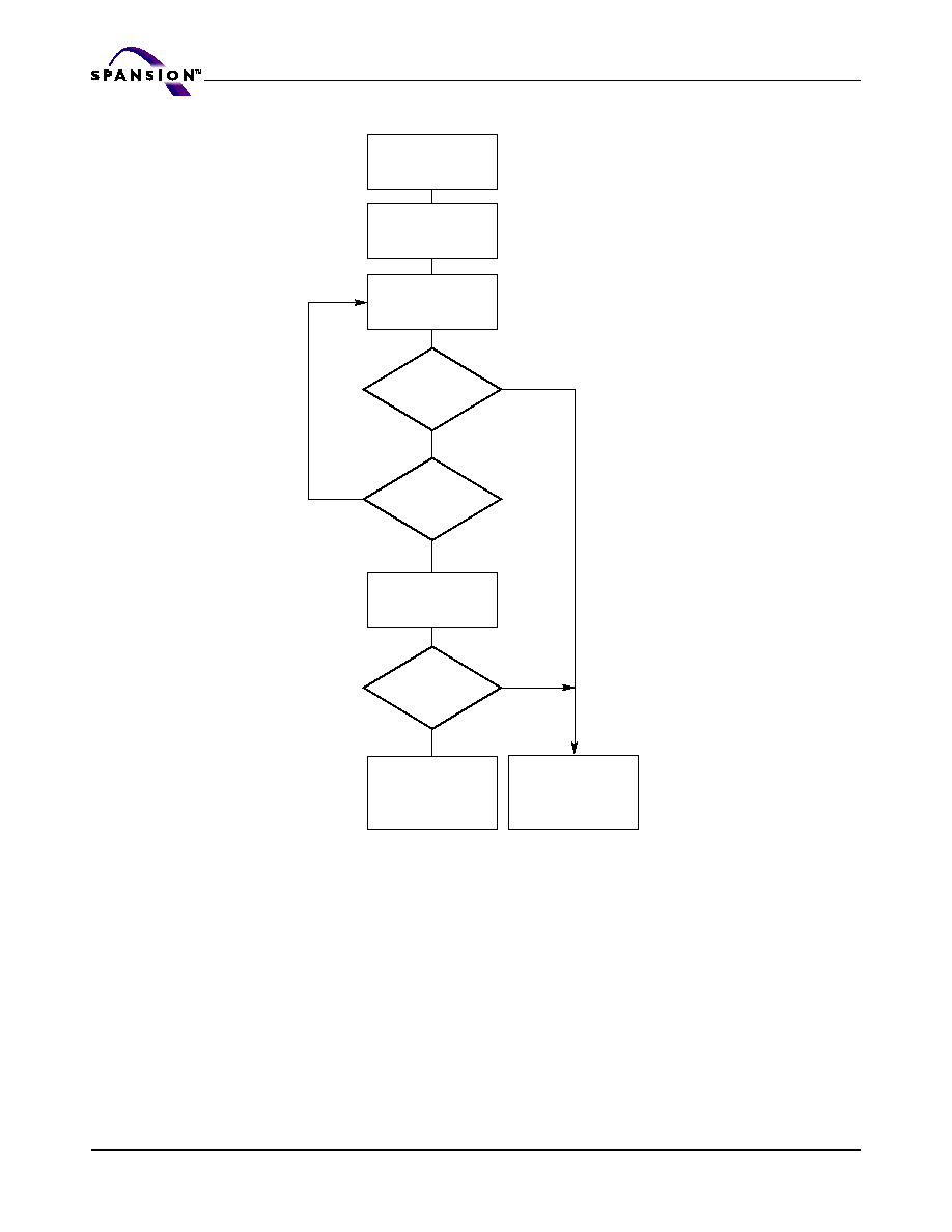
60
S71GL032A Based MCPs
S71GL032A_00_A0 March 31, 2005
A d v a n c e I n f o r m a t i o n
Notes:
1. The system should recheck the toggle bit even if DQ5 = "1" because the toggle bit may stop toggling as DQ5 changes
to "1." See the subsections on DQ6 and DQ2 for more information.
Figure 8. Toggle Bit Algorithm
START
No
Yes
Yes
DQ5 = 1?
No
Yes
Toggle Bit
= Toggle?
No
Program/Erase
Operation Not
Complete, Write
Reset Command
Program/Erase
Operation Complete
Toggle Bit
= Toggle?
Read Byte Twice
(DQ7≠DQ0)
Address = VA
Read Byte
(DQ7≠DQ0)
Address =VA
Read Byte
(DQ7≠DQ0)
Address =VA

March 31, 2005 S71GL032A_00_A0
S71GL032A Based MCPs
61
A d v a n c e I n f o r m a t i o n
DQ2: Toggle Bit II
The "Toggle Bit II" on DQ2, when used with DQ6, indicates whether a particular
sector is actively erasing (that is, the Embedded Erase algorithm is in progress),
or whether that sector is erase-suspended. Toggle Bit II is valid after the rising
edge of the final WE# pulse in the command sequence.
DQ2 toggles when the system reads at addresses within those sectors that have
been selected for erasure. (The system may use either OE# or CE# to control the
read cycles.) But DQ2 cannot distinguish whether the sector is actively erasing or
is erase-suspended. DQ6, by comparison, indicates whether the device is actively
erasing, or is in Erase Suspend, but cannot distinguish which sectors are selected
for erasure. Thus, both status bits are required for sector and mode information.
Refer to
Table 23
to compare outputs for DQ2 and DQ6.
Figure 8
shows the toggle bit algorithm in flowchart form, and the section "DQ2:
Toggle Bit II" explains the algorithm. See also the RY/BY#: Ready/Busy# subsec-
tion.
Figure 20
shows the toggle bit timing diagram.
Figure 21
shows the
differences between DQ2 and DQ6 in graphical form.
Reading Toggle Bits DQ6/DQ2
Refer to
Figure 8
for the following discussion. Whenever the system initially be-
gins reading toggle bit status, it must read DQ7≠DQ0 at least twice in a row to
determine whether a toggle bit is toggling. Typically, the system would note and
store the value of the toggle bit after the first read. After the second read, the
system would compare the new value of the toggle bit with the first. If the toggle
bit is not toggling, the device has completed the program or erase operation. The
system can read array data on DQ7≠DQ0 on the following read cycle.
However, if after the initial two read cycles, the system determines that the toggle
bit is still toggling, the system also should note whether the value of DQ5 is high
(see the section on DQ5). If it is, the system should then determine again
whether the toggle bit is toggling, since the toggle bit may have stopped toggling
just as DQ5 went high. If the toggle bit is no longer toggling, the device has suc-
cessfully completed the program or erase operation. If it is still toggling, the
device did not completed the operation successfully, and the system must write
the reset command to return to reading array data.
The remaining scenario is that the system initially determines that the toggle bit
is toggling and DQ5 has not gone high. The system may continue to monitor the
toggle bit and DQ5 through successive read cycles, determining the status as de-
scribed in the previous paragraph. Alternatively, it may choose to perform other
system tasks. In this case, the system must start at the beginning of the algo-
rithm when it returns to determine the status of the operation (top of
Figure 8
).
DQ5: Exceeded Timing Limits
DQ5 indicates whether the program, erase, or write-to-buffer time has ex-
ceeded a specified internal pulse count limit. Under these conditions DQ5
produces a "1," indicating that the program or erase cycle was not successfully
completed.
The device may output a "1" on DQ5 if the system tries to program a "1" to a
location that was previously programmed to "0." Only an erase operation can
change a "0" back to a "1." Under this condition, the device halts the opera-
tion, and when the timing limit has been exceeded, DQ5 produces a "1."

62
S71GL032A Based MCPs
S71GL032A_00_A0 March 31, 2005
A d v a n c e I n f o r m a t i o n
In all these cases, the system must write the reset command to return the device
to the reading the array (or to erase-suspend-read if the device was previously
in the erase-suspend-program mode).
DQ3: Sector Erase Timer
After writing a sector erase command sequence, the system may read DQ3 to de-
termine whether or not erasure has begun. (The sector erase timer does not
apply to the chip erase command.) If additional sectors are selected for erasure,
the entire time-out also applies after each additional sector erase command.
When the time-out period is complete, DQ3 switches from a "0" to a "1." If the
time between additional sector erase commands from the system can be as-
sumed to be less than 50 µs, the system need not monitor DQ3. See also the
Sector Erase Command Sequence section.
After the sector erase command is written, the system should read the status of
DQ7 (Data# Polling) or DQ6 (Toggle Bit I) to ensure that the device has accepted
the command sequence, and then read DQ3. If DQ3 is "1," the Embedded Erase
algorithm has begun; all further commands (except Erase Suspend) are ignored
until the erase operation is complete. If DQ3 is "0," the device will accept addi-
tional sector erase commands. To ensure the command has been accepted, the
system software should check the status of DQ3 prior to and following each sub-
sequent sector erase command. If DQ3 is high on the second status check, the
last command might not have been accepted.
Table 23
shows the status of DQ3 relative to the other status bits.
DQ1: Write-to-Buffer Abort
DQ1 indicates whether a Write-to-Buffer operation was aborted. Under these
conditions DQ1 produces a "1". The system must issue the Write-to-Buffer-Abort-
Reset command sequence to return the device to reading array data. See Write
Buffer section for more details.

March 31, 2005 S71GL032A_00_A0
S71GL032A Based MCPs
63
A d v a n c e I n f o r m a t i o n
Notes:
1. DQ5 switches to `1' when an Embedded Program, Embedded Erase, or Write-to-Buffer operation has exceeded the
maximum timing limits. Refer to the section on DQ5 for more information.
2. DQ7 and DQ2 require a valid address when reading status information. Refer to the appropriate subsection for
further details.
3. The Data# Polling algorithm should be used to monitor the last loaded write-buffer address location.
4. DQ1 switches to `1' when the device has aborted the write-to-buffer operation.
Table 23. Write Operation Status
Status
DQ7
(Note 2)
DQ6
DQ5
(Note 1)
DQ3
DQ2
(Note 2)
DQ1
RY/
BY#
Standard
Mode
Embedded Program Algorithm
DQ7#
Toggle
0
N/A
No toggle
0
0
Embedded Erase Algorithm
0
Toggle
0
1
Toggle
N/A
0
Program
Suspend
Mode
Program-
Suspend
Read
Program-Suspended
Sector
Invalid (not allowed)
1
Non-Program
Suspended Sector
Data
1
Erase
Suspend
Mode
Erase-
Suspend
Read
Erase-Suspended
Sector
1
No toggle
0
N/A
Toggle
N/A
1
Non-Erase
Suspended Sector
Data
1
Erase-Suspend-Program
(Embedded Program)
DQ7#
Toggle
0
N/A
N/A
N/A
0
Write-to-
Buffer
Busy (Note 3)
DQ7#
Toggle
0
N/A
N/A
0
0
Abort (Note 4)
DQ7#
Toggle
0
N/A
N/A
1
0
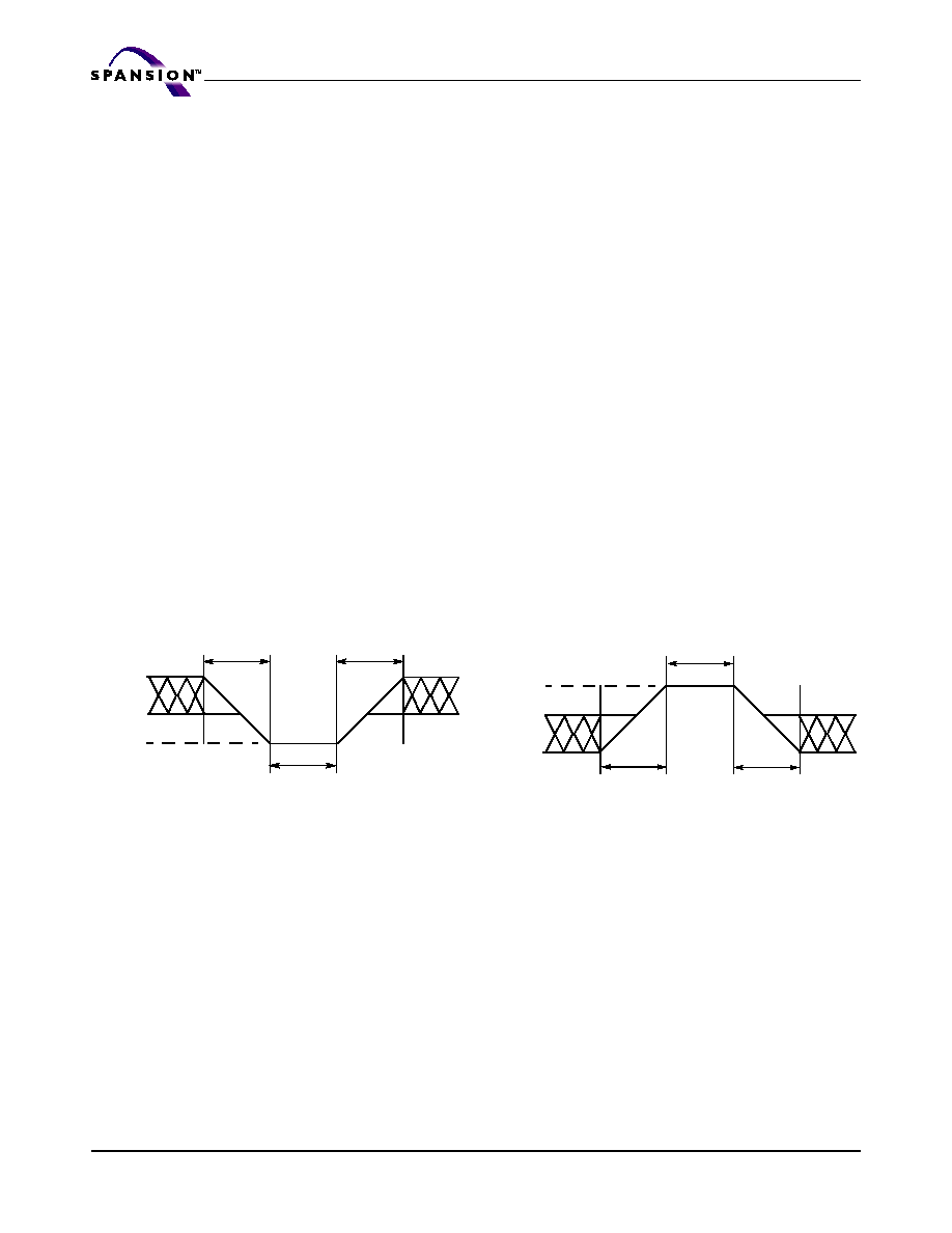
64
S71GL032A Based MCPs
S71GL032A_00_A0 March 31, 2005
A d v a n c e I n f o r m a t i o n
Absolute Maximum Ratings
Storage Temperature, Plastic Packages . . . . . . . . . . . . . . . . ≠65∞C to +150∞C
Ambient Temperature with Power Applied . . . . . . . . . . . . . . ≠65∞C to +125∞C
Voltage with Respect to Ground:
V
CC
(Note 1). . . . . . . . . . . . . . . . . . . . . . . . . . . . . . .≠0.5 V to +4.0 V
ACC and RESET# (Note 2) . . . . . . . . . . . . . . . . . . . . ≠0.5 V to +12.5 V
All other pins (Note 1) . . . . . . . . . . . . . . . . . . . . . ≠0.5 V to V
CC
+0.5 V
Output Short Circuit Current (Note 3). . . . . . . . . . . . . . . . . . . . . . . . 200 mA
Notes:
1. Minimum DC voltage on input or I/Os is ≠0.5 V. During voltage transitions, inputs
or I/Os may overshoot V
SS
to ≠2.0 V for periods of up to 20 ns. See
Figure 9
.
Maximum DC voltage on input or I/Os is V
CC
+ 0.5 V. During voltage transitions,
input or I/O pins may overshoot to V
CC
+ 2.0 V for periods up to 20 ns. See
Figure
10
.
2. Minimum DC input voltage on pins A9, OE#, ACC, and RESET# is ≠0.5 V. During
voltage transitions, A9, OE#, ACC, and RESET# may overshoot V
SS
to ≠2.0 V for
periods of up to 20 ns. See
Figure 9
. Maximum DC input voltage on pin A9, OE#,
ACC, and RESET# is +12.5 V which may overshoot to +14.0V for periods up to
20 ns.
3. No more than one output may be shorted to ground at a time. Duration of the short
circuit should not be greater than one second.
4. Stresses above those listed under "Absolute Maximum Ratings" may cause
permanent damage to the device. This is a stress rating only; functional operation
of the device at these or any other conditions above those indicated in the
operational sections of this data sheet is not implied. Exposure of the device to
absolute maximum rating conditions for extended periods may affect device
reliability.
Operating Ranges
Industrial (I) Devices
Ambient Temperature (T
A
) . . . . . . . . . . . . . . . . . . . . . . . . . ≠40∞C to +85∞C
Supply Voltages
V
CC
for full voltage range . . . . . . . . . . . . . . . . . . . . . . . . . +2.7 V to +3.6 V
V
CC
for regulated voltage range . . . . . . . . . . . . . . . . . . . . . +3.0 V to +3.6 V
V
IO
. . . . . . . . . . . . . . . . . . . . . . . . . . . . . . . . . . . . . . . . . . . . . . . . V
CC
Note:Operating ranges define those limits between which the functionality of the device is guaranteed.
Figure 9. Maximum Negative
Overshoot Waveform
Figure 10. Maximum Positive
Overshoot Waveform
20 ns
20 ns
+0.8 V
≠0.5 V
20 ns
≠2.0 V
20 ns
20 ns
V
CC
+2.0 V
V
CC
+0.5 V
20 ns
2.0 V

March 31, 2005 S71GL032A_00_A0
S71GL032A Based MCPs
65
A d v a n c e I n f o r m a t i o n
DC Characteristics
CMOS Compatible
Notes:
1. On the WP#/ACC pin only, the maximum input load current when WP# = V
IL
is ± 5.0 µA.
2. The I
CC
current listed is typically less than 3.5 mA/MHz, with OE# at V
IH
.
3. Maximum I
CC
specifications are tested with V
CC
= V
CC
max.
4. I
CC
active while Embedded Erase or Embedded Program is in progress.
5. Automatic sleep mode enables the low power mode when addresses remain stable for t
ACC
+ 30 ns.
6. V
CC
voltage requirements.
7. Not 100% tested.
Parameter
Symbol
Parameter Description (Notes)
Test Conditions
Min
Typ
Max
Unit
I
LI
Input Load Current (Note 1)
V
IN
= V
SS
to V
CC
,
V
CC
= V
CC
max
±1.0
µA
I
LIT
A9, ACC Input Load Current
V
CC
= V
CC max
; A9 =
12.5 V
-40∞C to 0∞C
250
µA
0∞C to 85∞C
35
I
LR
Reset Leakage Current
V
CC
= V
CC max
; RESET# = 12.5 V
35
µA
I
LO
Output Leakage Current
V
OUT
= V
SS
to V
CC
,
V
CC
= V
CC max
±1.0
µA
I
CC1
V
CC
Initial Read Current (Notes 2, 3)
CE# = V
IL,
OE# =
V
IH
,
1 MHz
5
20
mA
5 MHz
18
25
10 MHz
35
50
I
CC2
V
CC
Intra-Page Read Current (Notes 2, 3)
CE# = V
IL,
OE# = V
IH
10 MHz
5
20
mA
40 MHz
10
40
I
CC3
V
CC
Active Write Current (Note 3)
CE# = V
IL,
OE# = V
IH
50
60
mA
I
CC4
V
CC
Standby Current (Note 3)
CE#, RESET# = V
CC
± 0.3 V,
WP# = V
IH
1
5
µA
I
CC5
V
CC
Reset Current (Note 3)
RESET# = V
SS
± 0.3 V, WP# = V
IH
1
5
µA
I
CC6
Automatic Sleep Mode (Notes 3, 5)
V
IH
= V
CC
± 0.3 V;
-0.1< V
IL
0.3 V, WP# = V
IH
1
5
µA
V
IL
Input Low Voltage 1 (Note 6)
≠0.5
0.8
V
V
IH
Input High Voltage 1 (Note 6)
0.7 V
CC
V
CC
+ 0.5
V
V
HH
Voltage for ACC Program
Acceleration
V
CC
= 2.7 ≠3.6 V
11.5
12.0
12.5
V
V
ID
Voltage for Autoselect and Temporary
Sector Unprotect
V
CC
= 2.7 ≠3.6 V
11.5
12.0
12.5
V
V
OL
Output Low Voltage (Note 6)
I
OL
= 4.0 mA, V
CC
= V
CC min
0.45
V
V
OH1
Output High Voltage
I
OH
= ≠2.0 mA, V
CC
= V
CC min
0.85
V
CC
V
V
OH2
I
OH
= ≠100 µA, V
CC
= V
CC min
V
CC
≠0.4
V
V
LKO
Low V
CC
Lock-Out Voltage (Note 7)
2.3
2.5
V

66
S71GL032A Based MCPs
S71GL032A_00_A0 March 31, 2005
A d v a n c e I n f o r m a t i o n
Test Conditions
Key to Switching Waveforms
Figure 12. Input Waveforms and Measurement Levels
Note: Diodes are IN3064 or equivalent.
Figure 11. Test Setup
Table 24. Test Specifications
2.7 k
C
L
6.2 k
3.3 V
Device
Under
Test
Test Condition
All Speeds
Unit
Output Load
1 TTL gate
Output Load Capacitance, C
L
(including jig capacitance)
30
pF
Input Rise and Fall Times
5
ns
Input Pulse Levels
0.0 or V
CC
V
Input timing measurement
reference levels (See Note)
0.5 V
CC
V
Output timing measurement
reference levels
0.5 V
CC
V
Waveform
Inputs
Outputs
Steady
Changing from H to L
Changing from L to H
Don't Care, Any Change Permitted
Changing, State Unknown
Does Not Apply
Center Line is High Impedance State (High Z)
VCC
0.0 V
Output
Measurement Level
Input
0.5 VCC
0.5 VCC

March 31, 2005 S71GL032A_00_A0
S71GL032A Based MCPs
67
A d v a n c e I n f o r m a t i o n
AC Characteristics
Read-Only Operations-S29GL064A only
Notes:
1. Not 100% tested.
2. See
Figure 11
and
Table 24
for test specifications.
Read-Only Operations-S29GL032A only
Notes:
1. Not 100% tested.
2. See
Figure 11
and
Table 24
for test specifications.
Parameter
Description
Test Setup
Speed Options
Unit
JEDEC
Std.
90
10
11
t
AVAV
t
RC
Read Cycle Time (Note 1)
Min
90
100
110
ns
t
AVQV
t
ACC
Address to Output Delay
CE#, OE# = V
IL
Max
90
100
110
ns
t
ELQV
t
CE
Chip Enable to Output Delay
OE# = V
IL
Max
90
100
110
ns
t
PACC
Page Access Time
Max
25
30
30
ns
t
GLQV
t
OE
Output Enable to Output Delay
Max
25
30
30
ns
t
EHQZ
t
DF
Chip Enable to Output High Z (Note 1)
Max
16
ns
t
GHQZ
t
DF
Output Enable to Output High Z (Note 1)
Max
16
ns
t
AXQX
t
OH
Output Hold Time From Addresses, CE# or OE#, Whichever Occurs
First
Min
0
ns
t
OEH
Output Enable Hold Time
(Note 1)
Read
Min
0
ns
Toggle and
Data# Polling
Min
10
ns
Parameter
Description
Test Setup
Speed Options
Unit
JEDEC
Std.
90
10
11
t
AVAV
t
RC
Read Cycle Time (Note 1)
Min
90
100
110
ns
t
AVQV
t
ACC
Address to Output Delay
CE#, OE# = V
IL
Max
90
100
110
ns
t
ELQV
t
CE
Chip Enable to Output Delay
OE# = V
IL
Max
90
100
110
ns
t
PACC
Page Access Time
Max
25
30
30
ns
t
GLQV
t
OE
Output Enable to Output Delay
Max
25
30
30
ns
t
EHQZ
t
DF
Chip Enable to Output High Z (Note 1)
Max
16
ns
t
GHQZ
t
DF
Output Enable to Output High Z (Note 1)
Max
16
ns
t
AXQX
t
OH
Output Hold Time From Addresses, CE# or OE#,
Whichever Occurs First
Min
0
ns
t
OEH
Output Enable Hold Time (Note 1)
Read
Min
0
ns
Toggle and
Data# Polling
Min
10
ns

68
S71GL032A Based MCPs
S71GL032A_00_A0 March 31, 2005
A d v a n c e I n f o r m a t i o n
Figure 13. Read Operation Timings
Note: * Figure shows device in word mode. Addresses are A1≠A-1 for byte mode.
Figure 14. Page Read Timings
t
OH
t
CE
Data
WE#
Addresses
CE#
OE#
HIGH Z
Valid Data
HIGH Z
Addresses Stable
t
RC
t
ACC
t
OEH
t
RH
t
OE
t
RH
0 V
RY/BY#
RESET#
t
DF
A23-A2
CE#
OE#
A1-A0*
Data Bus
Same Page
Aa
Ab
Ac
Ad
Qa
Qb
Qc
Qd
t
ACC
t
PACC
t
PACC
t
PACC
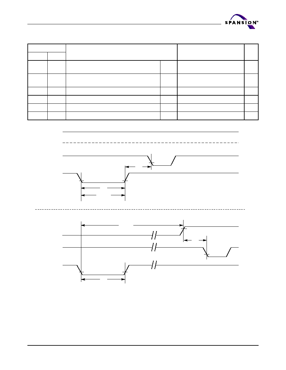
March 31, 2005 S71GL032A_00_A0
S71GL032A Based MCPs
69
A d v a n c e I n f o r m a t i o n
Hardware Reset (RESET#)
Note:Not 100% tested.
Notes:
1. Not 100% tested.
2. See the "Erase and Programming Performance" section for more information.
3. For 1≠16 words/1≠32 bytes programmed.
Figure 15. Reset Timings
Parameter
Description
All Speed Options
Unit
JEDEC
Std.
t
Ready
RESET# Pin Low (During Embedded Algorithms)
to Read Mode (See Note)
Max
20
µs
t
Ready
RESET# Pin Low (NOT During Embedded
Algorithms) to Read Mode (See Note)
Max
500
ns
t
RP
RESET# Pulse Width
Min
500
ns
t
RH
Reset High Time Before Read (See Note)
Min
50
ns
t
RPD
RESET# Input Low to Standby Mode (See Note)
Min
20
µs
t
RB
RY/BY# Output High to CE#, OE# pin Low
Min
0
ns
RESET#
RY/BY#
RY/BY#
t
RP
t
Ready
Reset Timings NOT during Embedded Algorithms
t
Ready
CE#, OE#
t
RH
CE#, OE#
Reset Timings during Embedded Algorithms
RESET#
t
RP
t
RB

70
S71GL032A Based MCPs
S71GL032A_00_A0 March 31, 2005
A d v a n c e I n f o r m a t i o n
Erase and Program Operations-S29GL064A Only
Notes:
1. Not 100% tested.
2. See the "Erase and Programming Performance" section for more information.
3. For 1≠16 words/1≠32 bytes programmed.
4. If a program suspend command is issued within t
POLL
, the device requires t
POLL
before reading status data, once
programming has resumed (that is, the program resume command has been written). If the suspend command was issued
after t
POLL
, status data is available immediately after programming has resumed. See
Figure 16
.
Parameter
Speed Options
Unit
JEDEC
Std.
Description
90
10
11
t
AVAV
t
WC
Write Cycle Time (Note 1)
Min
90
100
110
ns
t
AVWL
t
AS
Address Setup Time
Min
0
ns
t
ASO
Address Setup Time to OE# low during toggle bit polling
Min
15
ns
t
WLAX
t
AH
Address Hold Time
Min
45
ns
t
AHT
Address Hold Time From CE# or OE# high during toggle bit polling
Min
0
ns
t
DVWH
t
DS
Data Setup Time
Min
35
ns
t
WHDX
t
DH
Data Hold Time
Min
0
ns
t
CEPH
CE# High during toggle bit polling
Min
20
ns
t
OEPH
OE# High during toggle bit polling
Min
20
ns
t
GHWL
t
GHWL
Read Recovery Time Before Write (OE# High to WE# Low)
Min
0
ns
t
ELWL
t
CS
CE# Setup Time
Min
0
ns
t
WHEH
t
CH
CE# Hold Time
Min
0
ns
t
WLWH
t
WP
Write Pulse Width
Min
35
ns
t
WHDL
t
WPH
Write Pulse Width High
Min
30
ns
t
WHWH1
t
WHWH1
Write Buffer Program Operation (Notes 2, 3)
Typ
240
µs
Single Word Program Operation (Note 2)
Typ
60
Accelerated Single Word Program Operation (Note 2)
Typ
54
t
WHWH2
t
WHWH2
Sector Erase Operation (Note 2)
Typ
0.5
sec
t
VHH
V
HH
Rise and Fall Time (Note 1)
Min
250
ns
t
VCS
V
CC
Setup Time (Note 1)
Min
50
µs
t
BUSY
WE# High to RY/BY# Low
Min
90
100
110
ns
t
POLL
Program Valid before Status Polling
Max
4
µs
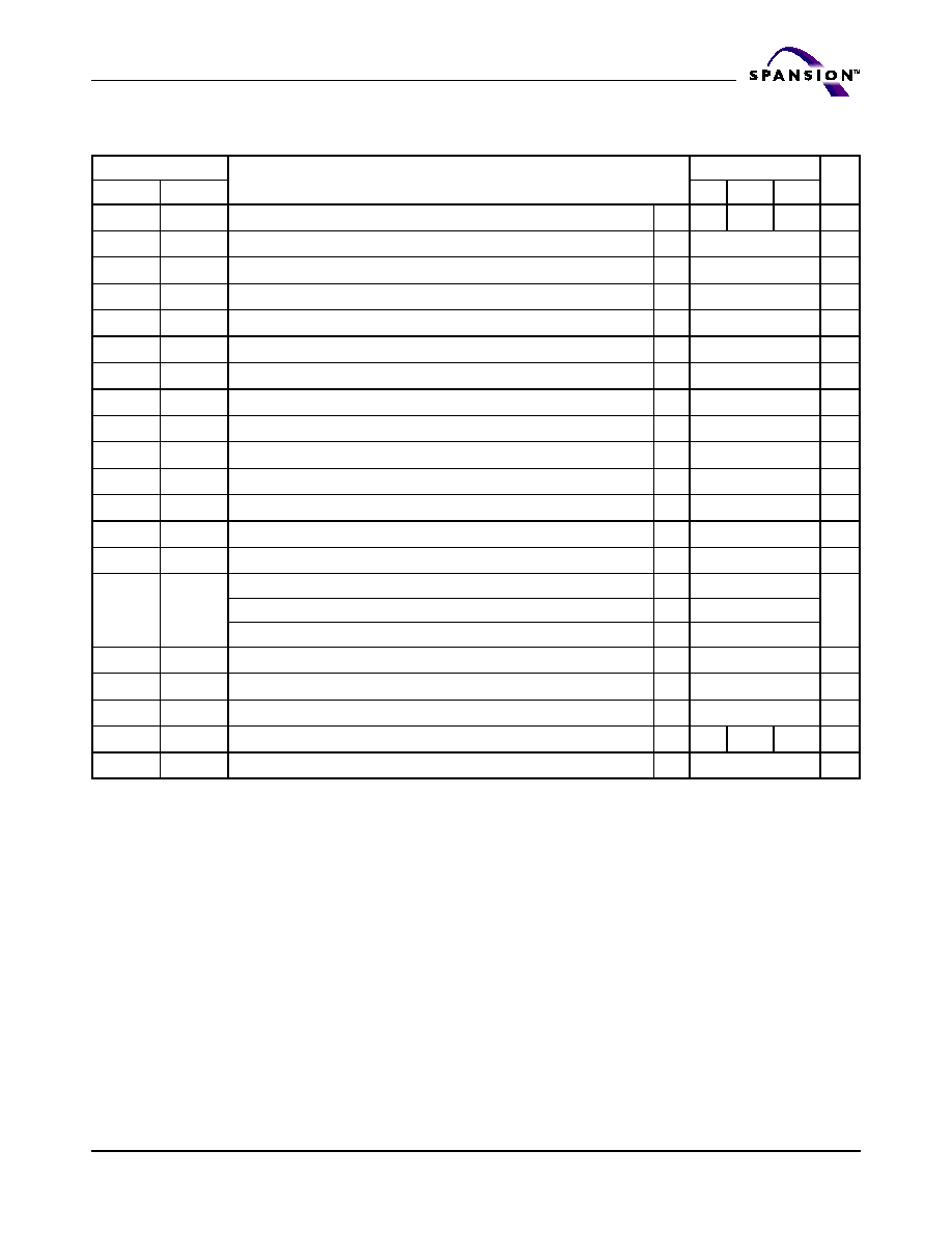
March 31, 2005 S71GL032A_00_A0
S71GL032A Based MCPs
71
A d v a n c e I n f o r m a t i o n
Erase and Program Operations-S29GL032A Only
Notes:
1. Not 100% tested.
2. See
"Erase And Programming Performance"
for more information
3. For 1≠16 words/1≠32 bytes programmed.
4. Effective write buffer specification is based upon a 16-word/32-byte write buffer operation.
5. If a program suspend command is issued within t
POLL
, the device requires t
POLL
before reading status data, once
programming resumes (that is, the program resume command has been written). If the suspend command was issued after
t
POLL
, status data is available immediately after programming resumes. See
Figure 16
.
Parameter
Description
Speed Options
Unit
JEDEC
Std.
90
10
11
t
AVAV
t
WC
Write Cycle Time (Note 1)
Min
90
100
110
ns
t
AVWL
t
AS
Address Setup Time
Min
0
ns
t
ASO
Address Setup Time to OE# low during toggle bit polling
Min
15
ns
t
WLAX
t
AH
Address Hold Time
Min
45
ns
t
AHT
Address Hold Time From CE# or OE# high during toggle bit polling
Min
0
ns
t
DVWH
t
DS
Data Setup Time
Min
35
ns
t
WHDX
t
DH
Data Hold Time
Min
0
ns
t
CEPH
CE# High during toggle bit polling
Min
20
ns
t
OEPH
OE# High during toggle bit polling
Min
20
ns
t
GHWL
t
GHWL
Read Recovery Time Before Write (OE# High to WE# Low)
Min
0
ns
t
ELWL
t
CS
CE# Setup Time
Min
0
ns
t
WHEH
t
CH
CE# Hold Time
Min
0
ns
t
WLWH
t
WP
Write Pulse Width
Min
35
ns
t
WHDL
t
WPH
Write Pulse Width High
Min
30
ns
t
WHWH1
t
WHWH1
Write Buffer Program Operation (Notes 2, 3)
Typ
240
µs
Single Word Program Operation (Note 2)
Typ
60
Accelerated Single Word Program Operation (Note 2)
Typ
54
t
WHWH2
t
WHWH2
Sector Erase Operation (Note 2)
Typ
0.5
sec
t
VHH
V
HH
Rise and Fall Time (Note 1)
Min
250
ns
t
VCS
V
CC
Setup Time (Note 1)
Min
50
µs
t
BUSY
WE# High to RY/BY# Low
Min
90
100
110
ns
t
POLL
Program Valid before Status Polling
Max
4
µs

72
S71GL032A Based MCPs
S71GL032A_00_A0 March 31, 2005
A d v a n c e I n f o r m a t i o n
Notes:
1. PA = program address, PD = program data, D
OUT
is the true data at the program address.
2. Illustration shows device in word mode.
Figure 16. Program Operation Timings
Figure 17. Accelerated Program Timing Diagram
OE#
WE#
CE#
V
CC
Data
Addresses
t
DS
t
AH
t
DH
t
WP
PD
t
WHWH1
t
WC
t
AS
t
WPH
t
VCS
555h
PA
PA
Read Status Data (last two cycles)
A0h
t
POLL
t
CS
Status
D
OUT
RY/BY#
t
RB
t
BUSY
t
CH
PA
Program Command Sequence (last two cycles)
ACC
t
VHH
V
HH
V
IL
or V
IH
V
IL
or V
IH
t
VHH
ACC
t
VHH
V
HH
V
IL
or V
IH
V
IL
or V
IH
t
VHH
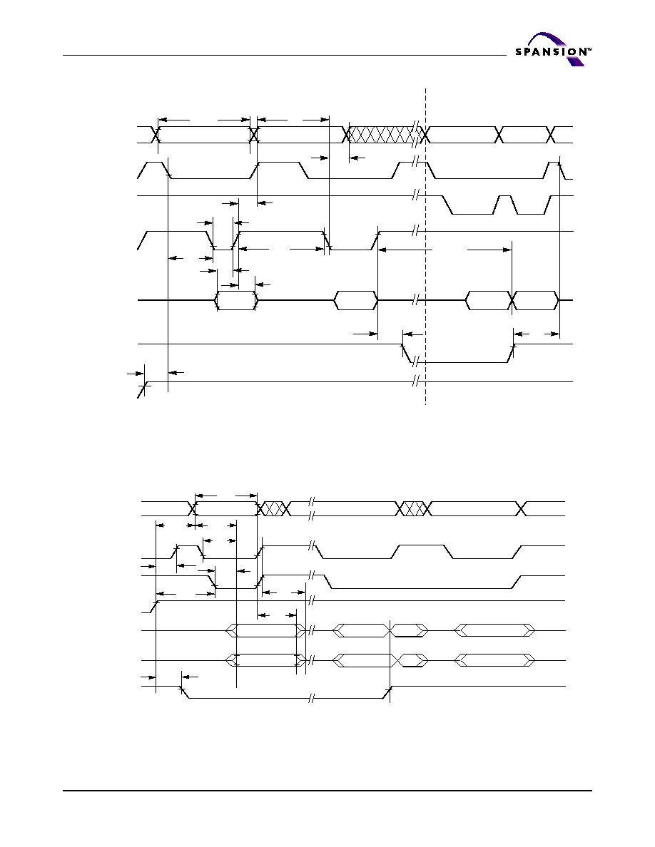
March 31, 2005 S71GL032A_00_A0
S71GL032A Based MCPs
73
A d v a n c e I n f o r m a t i o n
Notes:
1. SA = sector address (for Sector Erase), VA = Valid Address for reading status data (see "Write Operation Status".)
2. Illustration shows device in word mode.
Figure 18. Chip/Sector Erase Operation Timings
Note: VA = Valid address. Illustration shows first status cycle after command sequence, last status read cycle, and array
data read cycle.
Figure 19. Data# Polling Timings (During Embedded Algorithms)
OE#
CE#
Addresses
V
CC
WE#
Data
2AAh
SA
t
AH
t
WP
t
WC
t
AS
t
WPH
555h for chip erase
10 for Chip Erase
30h
t
DS
t
VCS
t
CS
t
DH
55h
t
CH
Status
D
OUT
t
WHWH2
VA
VA
Erase Command Sequence (last two cycles)
Read Status Data
RY/BY#
t
RB
t
BUSY
WE#
CE#
OE#
High Z
t
OE
High Z
DQ7
DQ0≠DQ6
RY/BY#
t
BUSY
Complement
True
Addresses
VA
t
CH
VA
VA
Status Data
Complement
Status Data
True
Valid Data
Valid Data
t
POLL
t
ACC
t
CE
t
OEH
t
DF
t
OH
t
RC
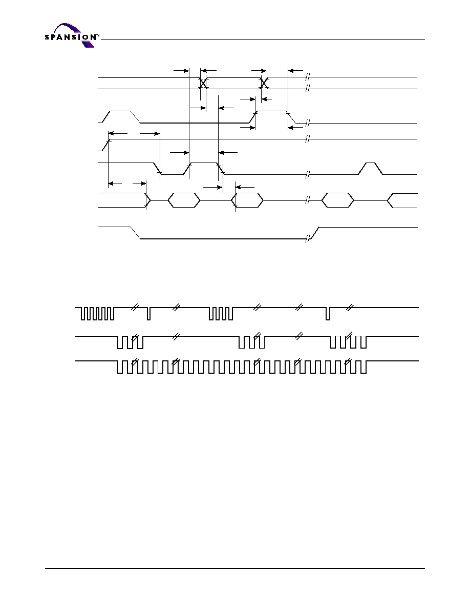
74
S71GL032A Based MCPs
S71GL032A_00_A0 March 31, 2005
A d v a n c e I n f o r m a t i o n
Note: VA = Valid address; not required for DQ6. Illustration shows first two status cycle after command sequence, last
status read cycle, and array data read cycle.
Figure 20. Toggle Bit Timings (During Embedded Algorithms)
Note: DQ2 toggles only when read at an address within an erase-suspended sector. The system may use OE# or CE#
to toggle DQ2 and DQ6.
Figure 21. DQ2 vs. DQ6
OE#
CE#
WE#
Addresses
t
OEH
t
DH
t
AHT
t
ASO
t
OEPH
t
OE
Valid Data
(first read)
(second read)
(stops toggling)
t
CEPH
t
AHT
t
AS
DQ6/DQ2
Valid Data
Valid
Status
Valid
Status
Valid
Status
RY/BY#
Enter
Erase
Erase
Erase
Enter Erase
Suspend Program
Erase Suspend
Read
Erase Suspend
Read
Erase
WE#
DQ6
DQ2
Erase
Complete
Erase
Suspend
Suspend
Program
Resume
Embedded
Erasing
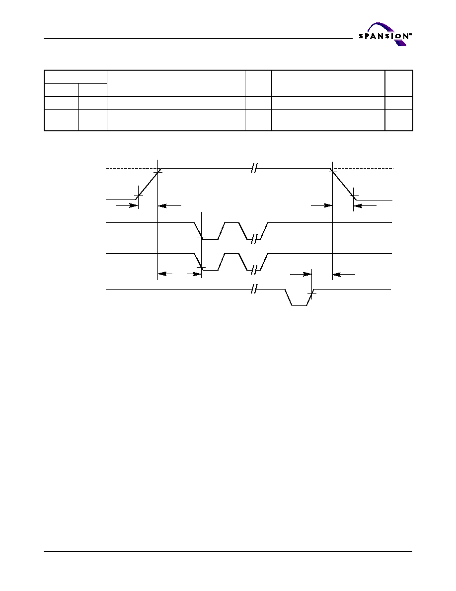
March 31, 2005 S71GL032A_00_A0
S71GL032A Based MCPs
75
A d v a n c e I n f o r m a t i o n
Temporary Sector Unprotect
Notes:
1. Not 100% tested.
Figure 22. Temporary Sector Group Unprotect Timing Diagram
Parameter
All Speed Options
JEDEC
Std
Description
Unit
t
VIDR
V
ID
Rise and Fall Time (See Note)
Min
500
ns
t
RSP
RESET# Setup Time for Temporary Sector
Unprotect
Min
4
µs
RESET#
t
VIDR
V
ID
V
IL
or V
IH
V
ID
V
IL
or V
IH
CE#
WE#
RY/BY#
t
VIDR
t
RSP
Program or Erase Command Sequence
t
RRB

76
S71GL032A Based MCPs
S71GL032A_00_A0 March 31, 2005
A d v a n c e I n f o r m a t i o n
Note: For sector group protect, A6:A0 = 0xx0010. For sector group unprotect, A6:A0 = 1xx0010.
Figure 23. Sector Group Protect and Unprotect Timing Diagram
Sector Group Protect: 150 µs,
Sector Group Unprotect: 15 ms
1 µs
RESET#
SA, A6,
A3, A2,
A1, A0
Data
CE#
WE#
OE#
60h
60h
40h
Valid*
Valid*
Valid*
Status
Sector Group Protect or Unprotect
Verify
V
ID
V
IH
March 31, 2005 S71GL032A_00_A0
S71GL032A Based MCPs
77
A d v a n c e I n f o r m a t i o n
AC Characteristics
Alternate CE# Controlled Erase and Program Operations-S29GL064A
Notes:
1. Not 100% tested.
2. See the "Erase and Programming Performance" section for more information.
3. For 1≠16 words/1≠32 bytes programmed.
4. If a program suspend command is issued within t
POLL
, the device requires t
POLL
before reading status data, once
programming has resumed (that is, the program resume command has been written). If the suspend command was issued
after t
POLL
, status data is available immediately after programming has resumed. See
Figure 24
.
Parameter
Speed Options
Unit
JEDEC
Std.
Description
90
10
11
t
AVAV
t
WC
Write Cycle Time (Note 1)
Min
90
100
110
ns
t
AVWL
t
AS
Address Setup Time
Min
0
ns
t
ELAX
t
AH
Address Hold Time
Min
45
ns
t
DVEH
t
DS
Data Setup Time
Min
35
ns
t
EHDX
t
DH
Data Hold Time
Min
0
ns
t
GHEL
t
GHEL
Read Recovery Time Before Write (OE# High to WE# Low)
Min
0
ns
t
WLEL
t
WS
WE# Setup Time
Min
0
ns
t
EHWH
t
WH
WE# Hold Time
Min
0
ns
t
ELEH
t
CP
CE# Pulse Width
Min
35
ns
t
EHEL
t
CPH
CE# Pulse Width High
Min
25
ns
t
WHWH1
t
WHWH1
Write Buffer Program Operation (Notes 2, 3)
Typ
240
µs
Single Word Program Operation (Note 2)
Typ
60
Accelerated Single Word Program Operation (Note 2)
Typ
54
t
WHWH2
t
WHWH2
Sector Erase Operation (Note 2)
Typ
0.5
sec
t
RH
RESET# High Time Before Write
Min
50
ns
t
POLL
Program Valid before Status Polling (Note 5)
Max
4
µs

78
S71GL032A Based MCPs
S71GL032A_00_A0 March 31, 2005
A d v a n c e I n f o r m a t i o n
Alternate CE# Controlled Erase and Program Operations-S29GL032A
Notes:
1. Not 100% tested.
2. See
"Erase And Programming Performance"
for more information
3. For 1≠16 words/1≠32 bytes programmed.
4. If a program suspend command is issued within t
POLL
, the device requires t
POLL
before reading status data, once
programming resumes (that is, the program resume command has been written). If the suspend command was issued after
t
POLL
, status data is available immediately after programming resumes. See
Figure 24
.
Parameter
Description
Speed Options
Unit
JEDEC
Std.
90
10
11
t
AVAV
t
WC
Write Cycle Time (Note 1)
Min
90
100
110
ns
t
AVWL
t
AS
Address Setup Time
Min
0
ns
t
ELAX
t
AH
Address Hold Time
Min
45
ns
t
DVEH
t
DS
Data Setup Time
Min
35
ns
t
EHDX
t
DH
Data Hold Time
Min
0
ns
t
GHEL
t
GHEL
Read Recovery Time Before Write
(OE# High to WE# Low)
Min
0
ns
t
WLEL
t
WS
WE# Setup Time
Min
0
ns
t
EHWH
t
WH
WE# Hold Time
Min
0
ns
t
ELEH
t
CP
CE# Pulse Width
Min
35
ns
t
EHEL
t
CPH
CE# Pulse Width High
Min
25
ns
t
WHWH1
t
WHWH1
Write Buffer Program Operation (Notes 2, 3)
Typ
240
µs
Single Word Program Operation (Note 2)
Typ
60
Accelerated Single Word Program Operation (Note 2)
Typ
54
t
WHWH2
t
WHWH2
Sector Erase Operation (Note 2)
Typ
0.5
sec
t
RH
RESET# High Time Before Write
Min
50
ns
t
POLL
Program Valid before Status Polling (Note 4)
Max
4
µs
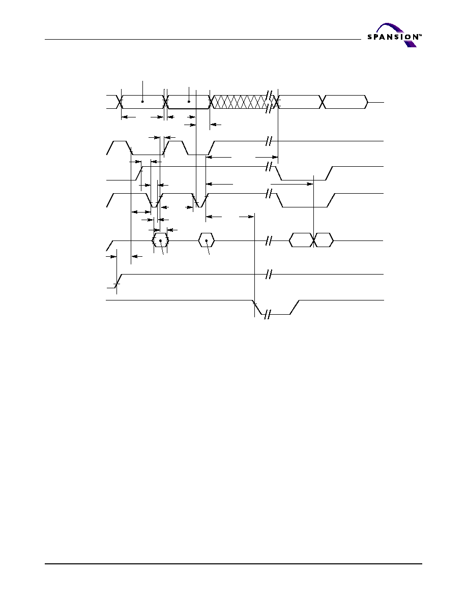
March 31, 2005 S71GL032A_00_A0
S71GL032A Based MCPs
79
A d v a n c e I n f o r m a t i o n
Notes:
1. Figure indicates last two bus cycles of a program or erase operation.
2. PA = program address, SA = sector address, PD = program data.
3. DQ7# is the complement of the data written to the device. D
OUT
is the data written to the device.
4. Illustration shows device in word mode.
Figure 24. Alternate CE# Controlled Write (Erase/Program) Operation Timings
t
GHEL
t
WS
OE#
CE#
WE#
RESET#
t
DS
Data
t
AH
Addresses
t
DH
t
CP
DQ7#
D
OUT
t
WC
t
AS
t
CPH
PA
Data# Polling
PBD for program
55 for erase
t
RH
t
WHWH1 or 2
t
POLL
RY/BY#
t
WH
29 for program buffer to flash
30 for sector erase
10 for chip erase
PBA for program
2AA for erase
SA for program buffer to flash
SA for sector erase
555 for chip erase
t
BUSY
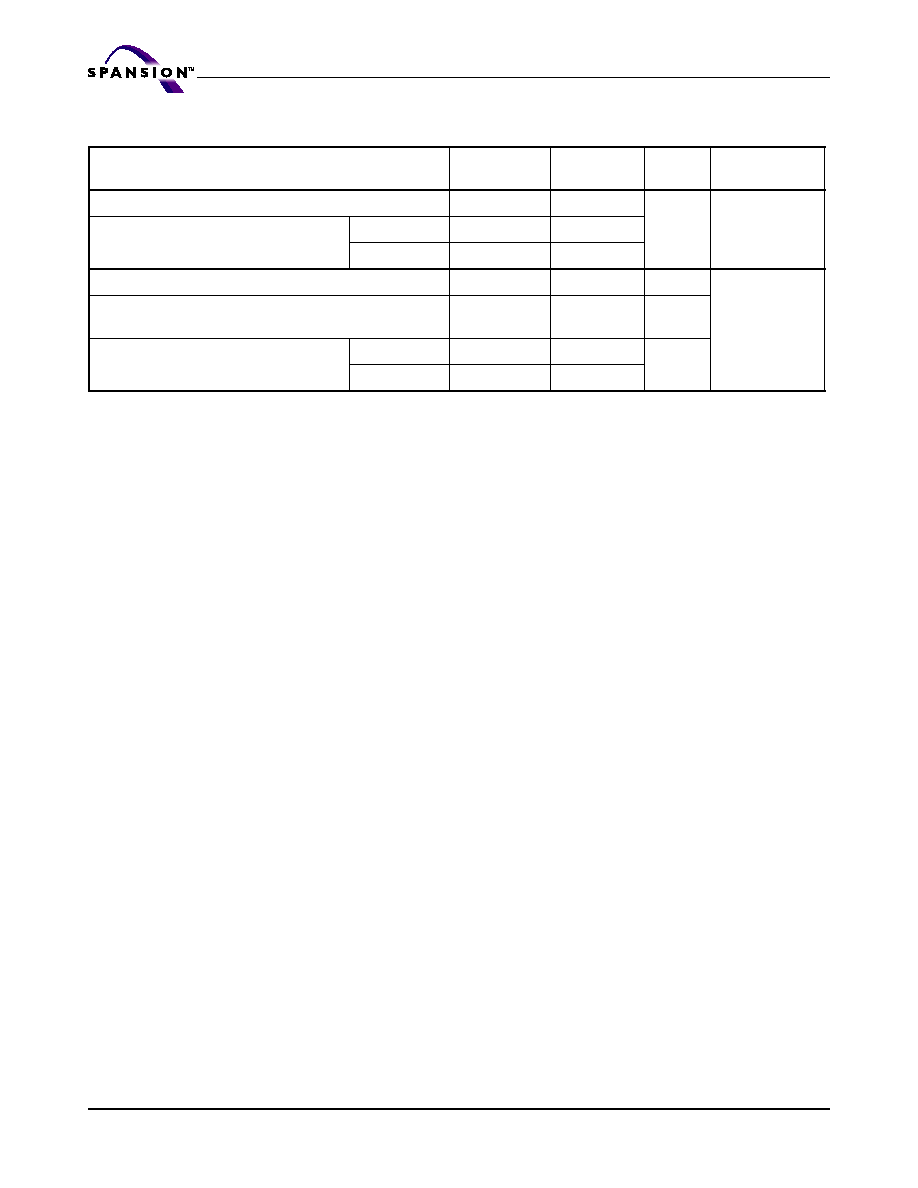
80
S71GL032A Based MCPs
S71GL032A_00_A0 March 31, 2005
A d v a n c e I n f o r m a t i o n
Erase And Programming Performance
Notes:
1. Typical program and erase times assume the following conditions: 25∞C, V
CC
= 3.0V, 10,000 cycles; checkerboard
data pattern.
2. Under worst case conditions of 90
∞
C; Worst case V
CC
, 100,000 cycles.
3. Effective programming time (typ) is 15 µs (per word), 7.5 µs (per byte).
4. Effective accelerated programming time (typ) is 12.5 µs (per word), 6.3 µs (per byte).
5. Effective write buffer specification is calculated on a per-word/per-byte basis for a 16-word/32-byte write buffer
operation.
6. In the pre-programming step of the Embedded Erase algorithm, all bits are programmed to 00h before erasure.
7. System-level overhead is the time required to execute the command sequence(s) for the program command. See
Table 22
for further information on command definitions.
Parameter
Typ (Note 1)
Max
(Note 2)
Unit
Comments
Sector Erase Time
0.5
3.5
sec
Excludes 00h
programming
prior to erasure
(Note 6)
Chip Erase Time
S29GL032A
32
64
S29GL064A
64
128
Total Write Buffer Program Time (Notes 3, 5)
240
µs
Excludes system
level overhead
(Note 7)
Total Accelerated Effective Write Buffer Program Time
(Notes 4, 5)
200
µs
Chip Program Time
S29GL032A
31.5
sec
S29GL064A
63

March 31, 2005 S71GL032A_00_A0
S71GL032A Based MCPs
81
A d v a n c e I n f o r m a t i o n
Type 4 pSRAM
4 Mbit (256K x 16)
Features
Wide voltage range: 2.7V to 3.3V
Typical active current: 3 mA @ f = 1 MHz
Low standby power
Automatic power-down when deselected
Functional Description
The Type 4 pSRAM is a high-performance CMOS pseudo static RAM (pSRAM) or-
ganized as 256K words by 16 bits that supports an asynchronous memory
interface. This device features advanced circuit design to provide ultra-low active
current. The device can be put into standby mode reducing power consumption
dramatically when deselected (CE1# Low, CE2 High or both BHE# and BLE# are
High). The input/output pins (I/O0 through I/O15) are placed in a high-imped-
ance state when: deselected (CE1# High, CE2 Low, OE# is deasserted High), or
during a write operation (Chip Enabled and Write Enable WE# Low). Reading
from the device is accomplished by asserting the Chip Enables (CE1# Low and
CE2 High) and Output Enable (OE#) Low while forcing the Write Enable (WE#)
High. If Byte Low Enable (BLE#) is Low, then data from the memory location
specified by the address pins will appear on I/O0 to I/O7. If Byte High Enable
(BHE#) is Low, then data from memory will appear on I/O8 to I/O15. See
Table
27
for a complete description of read and write modes.
Product Portfolio
Notes:
1. Typical values are included for reference only and are not guaranteed or tested. Typical values are measured at V
CC
= V
CC
(typ) and T
A
= 25∞C.
V
CC
Range (V)
Speed
(ns)
Power Dissipation
Operating, I
CC
(mA)
Standby (I
SB2
) (µA)
f = 1 MHz
f = f
max
Min
Typ
Max
Typ. (note 1)
Max
Typ. (note 1)
Max
Typ. (note 1)
Max
2.7V
3.0V
3.3V
70 ns
3
5
TBD
25 mA
15
40

82
S71GL032A Based MCPs
S71GL032A_00_A0 March 31, 2005
A d v a n c e I n f o r m a t i o n
Maximum Ratings
(Above which the useful life may be impaired. For user guidelines, not tested)
Storage Temperature . . . . . . . . . . . . . . . . . . . . . . . . . . . . -65∞C to +150∞C
Ambient Temperature with Power Applied . . . . . . . . . . . . . . . -40∞C to +85∞C
Supply Voltage to Ground Potential . . . . . . . . . . . . . . . . . . . . . -0.4V to 4.6V
DC Voltage Applied to Outputs in High-Z
State (note 1, 2, 3) . . . . . . . . . . . . . . . . . . . . . . . . . . . . . . . . -0.4V to 3.7V
DC Input Voltage (note 1, 2, 3) . . . . . . . . . . . . . . . . . . . . . . . . -0.4V to 3.7V
Output Current into Outputs (Low). . . . . . . . . . . . . . . . . . . . . . . . . . . 20 mA
Static Discharge Voltage . . . . . . . . . >2001V (per MIL-STD-883, Method 3015)
Latch-up Current . . . . . . . . . . . . . . . . . . . . . . . . . . . . . . . . . . . . . >200 mA
Notes:
1. V
IH(MAX)
= V
CC
+ 0.5V for pulse durations less than 20 ns.
2. V
IL(MIN)
= ≠0.5V for pulse durations less than 20 ns.
3. Overshoot and undershoot specifications are characterized and are not 100% tested.
Operating Range
Table 25. DC Electrical Characteristics (Over the Operating Range)
Notes:
1. Typical values are included for reference only and are not guaranteed or tested. Typical values are measured at V
CC
=
V
CC(typ.)
, T
A
= 25∞C.
Ambient Temperature (T
A
)
V
CC
-25∞C to +85∞C
2.7V to 3.3V
Parameter
Description
Test Conditions
Min.
Typ.
(note 1)
Max
Unit
V
CC
Supply Voltage
2.7
3.3
V
V
OH
Output High Voltage
I
OH
= ≠1.0 mA
V
CC
- 0.4
V
OL
Output Low Voltage
I
OL
= 0.1 mA
0.4
V
IH
Input High Voltage
0.8 * V
CC
V
CC
+ 0.4
V
IL
Input Low Voltage
F = 0
-0.4
0.4
I
IX
Input Leakage Current
GND V
IN
V
CC
-1
+1
µA
I
OZ
Output Leakage Current
GND V
OUT
V
CC
, Output Disabled
-1
+1
I
CC
V
CC
Operating Supply Current
f = f
MAX
= 1/t
RC
V
CC
= 3.3V
I
OUT
= 0 mA
CMOS Levels
TBD
15
mA
f = 1 MHz
3
I
SB1
Automatic CE# Power-Down
Current--CMOS Inputs
CE# V
CC
≠ 0.2V, CE2 0.2V
V
IN
V
CC
≠ 0.2V, V
IN
0.2V,
f = f
max
(Address and Data Only),
f=0 (OE#, WE#, BHE# and BLE#)
250
µA
I
SB2
Automatic CE# Power-Down
Current--CMOS Inputs
CE# V
CC
≠ 0.2V, CE2 0.2V
V
IN
V
CC
≠ 0.2V or V
IN
0.2V,
f = 0, V
CC
= 3.3V
40
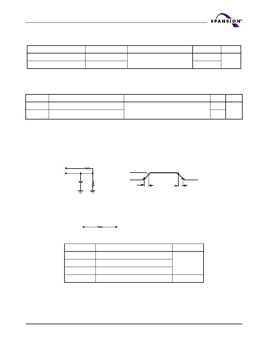
March 31, 2005 S71GL032A_00_A0
S71GL032A Based MCPs
83
A d v a n c e I n f o r m a t i o n
Capacitance
Note: Tested initially and after any design or process changes that may affect these parameters.
Thermal Resistance
Note: Tested initially and after any design or process changes that may affect these parameters.
AC Test Loads and Waveforms
Parameter
Description
Test Condition
Max
Unit
C
IN
Input Capacitance
T
A
= 25∞C, f = 1 MHz,
V
CC
= V
CC(typ.)
8
pF
C
OUT
Output Capacitance
8
Parameter
Description
Test Conditions
VFBGA
Unit
JA
Thermal Resistance (Junction to Ambient) Test conditions follow standard test methods
and procedures for measuring thermal
impedance, per EIA / JESD51.
55
∞C/W
JC
Thermal Resistance (Junction to Case)
17
Figure 25. AC Test Loads and Waveforms
Parameters
3.0V V
CC
Unit
R1
22000
R2
22000
R
TH
11000
V
TH
1.50
V
V
CC
V
CC
OUTPUT
R2
30 pF
INCLUDING
JIG AND
SCOPE
GND
90%
10%
90%
10%
OUTPUT
V
TH
Equivalent to:
TH… VENIN EQUIVALENT
ALL INPUT PULSES
R
T H
R1
Rise Time: 1 V/ns
Fall Time: 1 V/ns
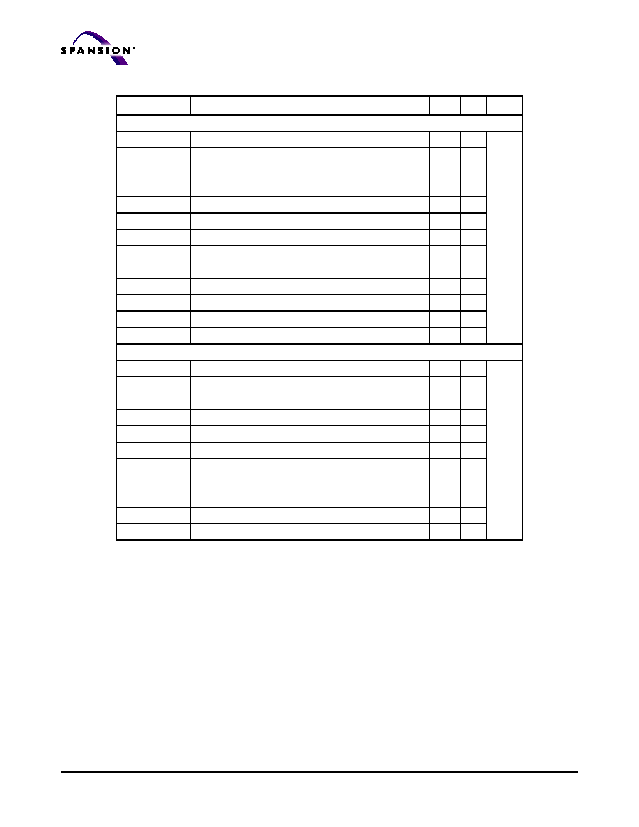
84
S71GL032A Based MCPs
S71GL032A_00_A0 March 31, 2005
A d v a n c e I n f o r m a t i o n
Table 26. Switching Characteristics
Notes:
1. Test conditions assume signal transition time of 1V/ns or higher, timing reference levels of V
CC(typ.)
/2, input pulse levels of
0 to V
CC(typ.)
, and output loading of the specified I
OL
/I
OH
and 30 pF load capacitance.
2. t
HZOE
, t
HZCE
, t
HZBE
and t
HZWE
transitions are measured when the outputs enter a high-impedance state.
3. High-Z and Low-Z parameters are characterized and are not 100% tested.
4. To achieve 55-ns performance, the read access should be CE# controlled. In this case t
ACE
is the critical parameter and t
SK
is
satisfied when the addresses are stable prior to chip enable going active. For the 70-ns cycle, the addresses must be stable
within 10 ns after the start of the read cycle.
5. The internal write time of the memory is defined by the overlap of WE#, CE#1 = V
IL
, CE2 = V
IH
, B
HE
and/or B
LE
=V
IL
. All
signals must be Active to initiate a write and any of these signals can terminate a write by going Inactive. The data input set-
up and hold timing should be referenced to the edge of the signal that terminates write.
Parameter
Description
Min
Max
Unit
Read Cycle
t
RC
Read Cycle Time
70
ns
t
AA
Address to Data Valid
70
t
OHA
Data Hold from Address Change
10
t
ACE
CE#1 Low and CE2 High to Data Valid
70
t
DOE
OE# Low to Data Valid
35
t
LZOE
OE# Low to Low Z (note 2, 3)
5
t
HZOE
OE# High to High Z (note 2, 3)
25
t
LZCE
CE#1 Low and CE2 High to Low Z (note 2, 3)
5
t
HZCE
CE#1 High and CE2 Low to High Z (note 2, 3)
25
t
DBE
BHE# / BLE# Low to Data Valid
70
t
LZBE
BHE# / BLE# Low to Low Z (note 2, 3)
5
t
HZBE
BHE# / BLE# High to High Z (note 2, 3)
25
t
SK
(note 4)
Address Skew
10
Write Cycle (note 5)
t
WC
Write Cycle Time
70
ns
t
SCE
CE#1 Low an CE2 High to Write End
55
t
AW
Address Set-Up to Write End
55
t
HA
Address Hold from Write End
0
t
SA
Address Set-Up to Write Start
0
t
PWE
WE# Pulse Width
55
t
BW
BLE# / BHE# LOW to Write End
55
t
SD
Data Set-up to Write End
25
t
HD
Data Hold from Write End
0
t
HZWE
WE# Low to High Z (note 2, 3)
25
t
LZWE
WE# High to Low Z (note 2, 3)
5

March 31, 2005 S71GL032A_00_A0
S71GL032A Based MCPs
85
A d v a n c e I n f o r m a t i o n
Switching Waveforms
Notes:
1. To achieve 55-ns performance, the read access should be CE# controlled. In this case t
ACE
is the critical parameter and t
SK
is
satisfied when the addresses are stable prior to chip enable going active. For the 70-ns cycle, the addresses must be stable
within 10 ns after the start of the read cycle.
2. Device is continuously selected. OE#, CE# = V
IL
.
3. WE# is High for Read Cycle.
Notes:
1. To achieve 55-ns performance, the read access should be CE# controlled. In this case t
ACE
is the critical parameter and t
SK
is
satisfied when the addresses are stable prior to chip enable going active. For the 70-ns cycle, the addresses must be stable
within 10 ns after the start of the read cycle.
2. WE# is High for Read Cycle.
Figure 26. Read Cycle 1 (Address Transition Controlled)
Figure 27. Read Cycle 2 (OE# Controlled)
ADDRESS
DATA OUT
PREVIOUS DATA VALID
DATA VALID
t
RC
tAA
tOHA
t
SK
DATA VALID
t
RC
t
ACE
t
DOE
t
LZOE
t
LZCE
HIGH IMPEDENCE
t
HZOE
HIGH
IMPEDENCE
ADDRESS
CE
2
t
HZBE
t
LZBE
t
HZCE
DATA OUT
t
DBE
t
SK
CE#1
BHE#/BLE#
OE#
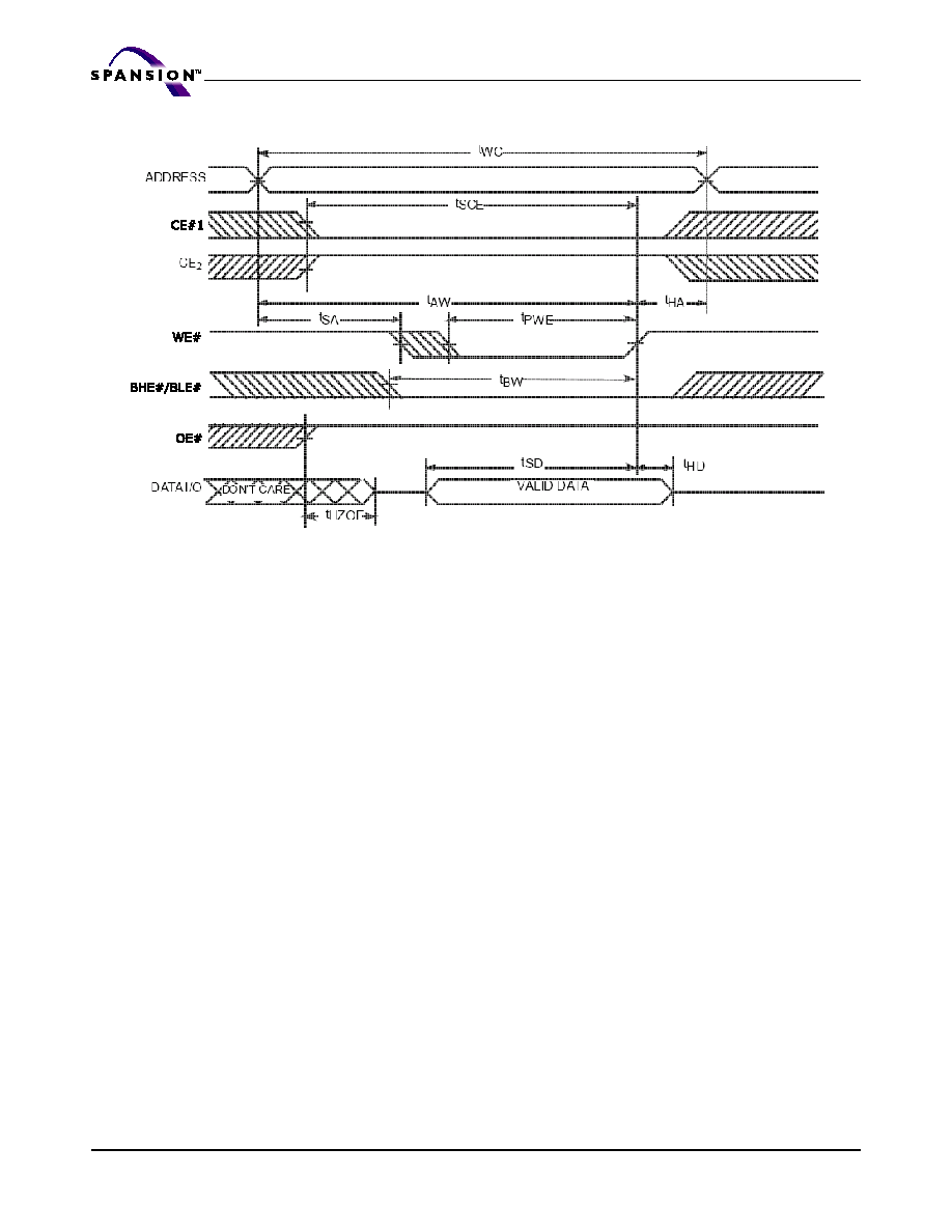
86
S71GL032A Based MCPs
S71GL032A_00_A0 March 31, 2005
A d v a n c e I n f o r m a t i o n
Notes:
1. High-Z and Low-Z parameters are characterized and are not 100% tested.
2. The internal write time of the memory is defined by the overlap of WE#, CE#1 = V
IL
, CE2 = V
IH
, B
HE
and/or B
LE
=V
IL
. All
signals must be Active to initiate a write and any of these signals can terminate a write by going Inactive. The data input set-
up and hold timing should be referenced to the edge of the signal that terminates write.
3. Data I/O is high impedance if OE#
V
IH
.
4. If Chip Enable goes Inactive simultaneously with WE# = High, the output remains in a high-impedance state.
5. During the Don't Care period in the Data I/O waveform, the I/Os are in output state and input signals should not be applied.
Figure 28. Write Cycle 1 (WE# Controlled)

March 31, 2005 S71GL032A_00_A0
S71GL032A Based MCPs
87
A d v a n c e I n f o r m a t i o n
Notes:
1. High-Z and Low-Z parameters are characterized and are not 100% tested.
2. The internal write time of the memory is defined by the overlap of WE#, CE#1 = V
IL
, CE2 = V
IH
, B
HE
and/or B
LE
=V
IL
. All
signals must be Active to initiate a write and any of these signals can terminate a write by going Inactive. The data input set-
up and hold timing should be referenced to the edge of the signal that terminates write.
3. Data I/O is high impedance if OE#
V
IH
.
4. If Chip Enable goes Inactive simultaneously with WE# = High, the output remains in a high-impedance state.
5. During the Don't Care period in the Data I/O waveform, the I/Os are in output state and input signals should not be applied.
Figure 29. Write Cycle 2 (CE#1 or CE2 Controlled)
t
HD
t
SD
t
PWE
t
HA
t
AW
t
SCE
t
WC
t
HZOE
ADDRESS
CE
2
DATA I/O
DON'T CARE
t
BW
t
SA
VALID DATA
CE#1
WE#
BHE#/BLE#
OE#
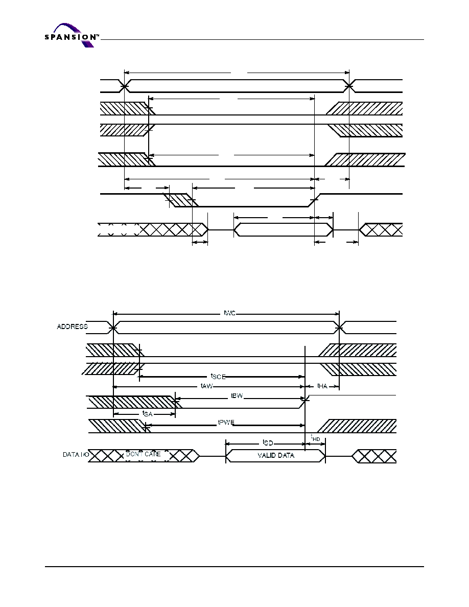
88
S71GL032A Based MCPs
S71GL032A_00_A0 March 31, 2005
A d v a n c e I n f o r m a t i o n
Notes:
1. If Chip Enable goes Inactive simultaneously with WE# = High, the output remains in a high-impedance state.
2. During the Don't Care period in the Data I/O waveform, the I/Os are in output state and input signals should not be applied.
Notes:
1. If Chip Enable goes Inactive simultaneously with WE# = High, the output remains in a high-impedance state.
2. During the Don't Care period in the Data I/O waveform, the I/Os are in output state and input signals should not be applied.
Figure 30. Write Cycle 3 (WE# Controlled, OE# Low)
Figure 31. Write Cycle 4 (BHE#/BLE# Controlled, OE# Low)
VALID DATA
t
HD
t
SD
t
LZWE
t
PWE
t
SA
t
HA
t
AW
t
SCE
t
WC
t
HZWE
ADDRESS
CE
2
DATA I/O
t
BW
DON'T CARE
CE#1
BHE#/BLE#
WE#
CE#1
CE2
BHE#/BLE#
WE#
March 31, 2005 S71GL032A_00_A0
S71GL032A Based MCPs
89
A d v a n c e I n f o r m a t i o n
Truth Table
Table 27. Truth Table
CE#1
CE2
WE# OE# BHE# BLE#
Inputs / Outputs
Mode
Power
H
X
X
X
X
X
High-Z
Deselect/Power-Down
Standby (I
SB
)
X
L
X
X
X
X
High-Z
X
X
X
X
H
H
High-Z
L
H
H
L
L
L
Data Out (I/O0≠I/O15)
Read (Upper Byte and Lower Byte)
Active (I
CC
)
L
H
H
L
H
L
Data Out (I/O0 ≠I/O7);
I/O8≠I/O15 in High Z
Read (Upper Byte only)
L
H
H
L
L
H
Data Out (I/O8≠I/O15);
I/O0≠I/O7 in High Z
Read (Lower Byte only)
L
H
H
H
L
L
High-Z
Output Disabled
L
H
H
H
H
L
High-Z
Output Disabled
L
H
H
H
L
H
High-Z
Output Disabled
L
H
L
X
L
L
Data In (I/O0≠I/O15)
Write (Upper Byte and Lower Byte)
L
H
L
X
H
L
Data In (I/O0≠I/O7);
I/O8≠I/O15 in High Z
Write (Lower Byte Only)
L
H
L
X
L
H
Data In (I/O8≠I/O15);
I/O0 ≠I/O7 in High Z
Write (Upper Byte Only)

90
S71GL032A Based MCPs
S71GL032A_00_A0 March 31, 2005
A d v a n c e I n f o r m a t i o n
Type 1 SRAM
4/8 Megabit CMOS SRAM
Common Features
Process Technology: Full CMOS
Power Supply Voltage: 2.7~3.3V
Three state outputs
Notes:
1. UB#, LB# swapping is available only at x16. x8 or x16 select by BYTE# pin.
Pin Description
Version
Density
Organization
(I
SB1
, Max.)
Standby
(I
CC2
, Max.)
Operating
Mode
F
4Mb
x8 or x16 (note 1)
10 µA
22 mA
Dual CS, UB# / LB# (tCS)
G
4Mb
x8 or x16 (note 1)
10 µA
22 mA
Dual CS, UB# / LB# (tCS)
C
8Mb
x8 or x16 (note 1)
15 µA
22 mA
Dual CS, UB# / LB# (tCS)
D
8Mb
X16
TBD
TBD
Dual CS, UB# / LB# (tCS)
Pin Name
Description
I/O
CS1#, CS2
Chip Selects
I
OE#
Output Enable
I
WE#
Write Enable
I
BYTE#
Word (V
CC
)/Byte (V
SS
) Select
I
A0~A17 (4M)
A0~A18 (8M)
Address Inputs
I
SA
Address Input for Byte Mode
I
I/O0~I/O15
Data Inputs/Outputs
I/O
V
CC
Power Supply
-
V
SS
Ground
-
DNU
Do Not Use
-
NC
No Connection
-
March 31, 2005 S71GL032A_00_A0
S71GL032A Based MCPs
91
A d v a n c e I n f o r m a t i o n
Functional Description
4M Version F, 4M version G, 8M version C
Note: X means don't care (must be low or high state).
Byte Mode
CS1# CS2 OE# WE#
BYTE#
SA
LB#
UB#
IO
0~7
IO
8~15
Mode
Power
H
X
X
X
X
X
X
X
High-Z
High-Z
Deselected
Standby
X
L
X
X
X
X
X
X
High-Z
High-Z
Deselected
Standby
X
X
X
X
X
X
H
H
High-Z
High-Z
Deselected
Standby
L
H
H
H
V
CC
X
L
X
High-Z
High-Z
Output Disabled
Active
L
H
H
H
V
CC
X
X
L
High-Z
High-Z
Output Disabled
Active
L
H
L
H
V
CC
X
L
H
D
out
High-Z
Lower Byte Read
Active
L
H
L
H
V
CC
X
H
L
High-Z
D
out
Upper Byte Read
Active
L
H
L
H
V
CC
X
L
L
D
out
D
out
Word Read
Active
L
H
X
L
V
CC
X
L
H
D
in
High-Z
Lower Byte Write
Active
L
H
X
L
V
CC
X
H
L
High-Z
D
in
Upper Byte Write
Active
L
H
X
L
V
CC
X
L
L
D
in
D
in
Word Write
Active
CS1# CS2 OE# WE#
BYTE#
SA
LB#
UB#
IO
0~7
IO
8~15
Mode
Power
H
X
X
X
X
X
X
X
High-Z
High-Z
Deselected
Standby
X
L
X
X
X
X
X
X
High-Z
High-Z
Deselected
Standby
L
H
H
H
X
X
H
H
High-Z
High-Z
Deselected
Standby
L
H
L
L
V
CC
X
L
X
High-Z
High-Z
Output Disabled
Active
L
H
X
L
V
CC
X
X
L
High-Z
High-Z
Output Disabled
Active
92
S71GL032A Based MCPs
S71GL032A_00_A0 March 31, 2005
A d v a n c e I n f o r m a t i o n
Functional Description
8M Version D
Note: X means don't care (must be low or high state).
Absolute Maximum Ratings (4M Version F)
Stresses greater than those listed under "Absolute Maximum Ratings" may cause permanent damage to the device. Functional
operation should be restricted to recommended operating condition. Exposure to absolute maximum rating conditions for
extended periods may affect reliability
.
Absolute Maximum Ratings (4M Version G, 8M Version C, 8M Version D)
Stresses greater than those listed under "Absolute Maximum Ratings" may cause permanent damage to the device. Functional
operation should be restricted to recommended operating condition. Exposure to absolute maximum rating conditions for
extended periods may affect reliability
.
CS1# CS2 OE# WE#
LB#
UB#
IO
0~8
IO
9~16
Mode
Power
H
X
X
X
X
X
High-Z
High-Z
Deselected
Standby
X
L
X
X
X
X
High-Z
High-Z
Deselected
Standby
X
X
X
X
H
H
High-Z
High-Z
Deselected
Standby
L
H
H
H
L
X
High-Z
High-Z
Output Disabled
Active
L
H
H
H
X
L
High-Z
High-Z
Output Disabled
Active
L
H
L
H
L
H
D
out
High-Z
Lower Byte Read
Active
L
H
L
H
H
L
High-Z
D
out
Upper Byte Read
Active
L
H
L
H
L
L
D
out
D
out
Word Read
Active
L
H
X
L
L
H
D
in
High-Z
Lower Byte Write
Active
L
H
X
L
H
L
High-Z
D
in
Upper Byte Write
Active
L
H
X
L
L
L
D
in
D
in
Word Write
Active
Item
Symbol
Ratings
Unit
Voltage on any pin relative to V
SS
V
IN
,V
OUT
-0.2 to V
CC
+0.3V
V
Voltage on V
CC
supply relative to V
SS
V
CC
-0.2 to 4.0V
V
Power Dissipation
P
D
1.0
W
Operating Temperature
T
A
-40 to 85
∞C
Item
Symbol
Ratings
Unit
Voltage on any pin relative to V
SS
V
IN
,V
OUT
-0.2 to V
CC
+0.3V (Max. 3.6V)
V
Voltage on V
CC
supply relative to V
SS
V
CC
-0.2 to 3.6V
V
Power Dissipation
P
D
1.0
W
Operating Temperature
T
A
-40 to 85
∞C
March 31, 2005 S71GL032A_00_A0
S71GL032A Based MCPs
93
A d v a n c e I n f o r m a t i o n
DC Characteristics
Recommended DC Operating Conditions (Note 1)
Notes:
1. T
A
= -40 to 85
∞
C, unless otherwise specified.
2. Overshoot: Vcc+1.0V in case of pulse width 20ns.
3. Undershoot: -1.0V in case of pulse width 20ns.
4. Overshoot and undershoot are sampled, not 100% tested.
Capacitance (f=1MHz, T
A
=25∞C)
Note: Capacitance is sampled, not 100% tested
DC Operating Characteristics
Common
Item
Symbol
Min
Typ
Max
Unit
Supply voltage
V
CC
2.7
3.0
3.3
V
Ground
V
SS
0
0
0
V
Input high voltage
V
IH
2.2
-
V
CC
+0.2 (Note 2)
V
Input low voltage
V
IL
-0.2 (Note 3)
-
0.6
V
Item
Symbol
Test Condition
Min
Max
Unit
Input capacitance
C
IN
V
IN
=0V
-
8
pF
Input/Output capacitance
C
IO
V
IO
=0V
-
10
pF
Item
Symbol
Test Conditions
Min
Typ
(Note)
Max
Unit
Input leakage current
I
LI
V
IN
=V
SS
to V
CC
-1
-
1
µA
Output leakage current
I
LO
CS1#=V
IH
or CS2=V
IL
or OE#=V
IH
or
WE#=V
IL
or LB#=UB#=V
IH
, V
IO
=V
ss
to V
CC
-1
-
1
µA
Output low voltage
V
OL
I
OL
= 2.1mA
-
-
0.4
V
Output high voltage
V
OH
I
OH
= -1.0mA
2.4
-
-
V

94
S71GL032A Based MCPs
S71GL032A_00_A0 March 31, 2005
A d v a n c e I n f o r m a t i o n
DC Operating Characteristics
4M Version F
Note: Typical values are not 100% tested.
DC Operating Characteristics
4M Version G
Note: Typical values are not 100% tested.
Item
Symbol
Test Conditions
Min
Typ
(Note)
Max
Unit
Average operating current
I
CC1
Cycle time=1µs, 100% duty, I
IO
=0mA, CS1# 0.2V,
CS2
V
CC
-0.2V,
BYTE#=V
SS
or V
CC
, V
IN
0.2V or V
IN
VCC-0.2V, LB#
0.2V or/and UB# 0.2V
-
-
3
mA
I
CC2
Cycle time=Min, I
IO
=0mA, 100% duty, CS1# = V
IL
,
CS2=V
IH
,
BYTE# = V
SS
or V
CC
, V
IN
=V
IL
or V
IH
, LB# 0.2V or/
and UB#
0.2V
-
-
22
mA
Standby Current (CMOS)
I
SB1
(Note)
CS1# V
CC
-0.2V, CS2 V
CC
-0.2V (CS1# controlled)
or CS2
0.2V (CS2 controlled), BYTE# = V
SS
or V
CC
,
Other input =0~V
CC
-
1.0
(Note)
10
µA
Item
Symbol
Test Conditions
Min
Typ
(Note)
Max
Unit
Average operating current
I
CC1
Cycle time=1µs, 100% duty, I
IO
=0mA, CS1# 0.2V,
CS2
V
CC
-0.2V,
BYTE#=V
SS
or V
CC
, V
IN
0.2V or V
IN
VCC-0.2V, LB#
0.2V or/and UB# 0.2V
-
-
4
mA
I
CC2
Cycle time=Min, I
IO
=0mA, 100% duty, CS1# = V
IL
,
CS2=V
IH
,
BYTE# = V
SS
or V
CC
, V
IN
=V
IL
or V
IH
, LB# 0.2V or/
and UB#
0.2V
-
-
22
mA
Standby Current (CMOS)
I
SB1
(Note)
CS1# V
CC
-0.2V, CS2 V
CC
-0.2V (CS1# controlled)
or CS2
0.2V (CS2 controlled), BYTE# = V
SS
or V
CC
,
Other input = 0~V
CC
-
3.0
(Note)
10
µA
March 31, 2005 S71GL032A_00_A0
S71GL032A Based MCPs
95
A d v a n c e I n f o r m a t i o n
DC Operating Characteristics
8M Version C
Note: Typical values are not 100% tested.
DC Operating Characteristics
8M Version D
Note: Typical values are not 100% tested.
Item
Symbol
Test Conditions
Min
Typ
(Note)
Max
Unit
Average operating current
I
CC1
Cycle time=1µs, 100% duty, I
IO
=0mA, CS1# 0.2V,
CS2
V
CC
-0.2V,
BYTE#=V
SS
or V
CC
, V
IN
0.2V or V
IN
VCC-0.2V, LB#
0.2V or/and UB# 0.2V
-
-
3
mA
I
CC2
Cycle time=Min, I
IO
=0mA, 100% duty, CS1# = V
IL
,
CS2=V
IH
,
BYTE# = V
SS
or V
CC
, V
IN
=V
IL
or V
IH
, LB# 0.2V or/
and UB#
0.2V
-
-
22
mA
Standby Current (CMOS)
I
SB1
(Note)
CS1# V
CC
-0.2V, CS2 V
CC
-0.2V (CS1# controlled)
or CS2
0.2V (CS2 controlled), BYTE# = V
SS
or V
CC
,
Other input = 0~V
CC
-
-
15
µA
Item
Symbol
Test Conditions
Min
Typ
(Note)
Max
Unit
Average operating current
I
CC1
Cycle time=1µs, 100% duty, I
IO
=0mA, CS1# 0.2V,
CS2
V
CC
-0.2V,
BYTE#=V
SS
or V
CC
, V
IN
0.2V or V
IN
VCC-0.2V, LB#
0.2V or/and UB# 0.2V
-
-
TBD
mA
I
CC2
Cycle time=Min, I
IO
=0mA, 100% duty, CS1# = V
IL
,
CS2=V
IH
,
BYTE# = V
SS
or V
CC
, V
IN
=V
IL
or V
IH
, LB# 0.2V or/
and UB#
0.2V
-
-
TBD
mA
Standby Current (CMOS)
I
SB1
(Note)
CS1# V
CC
-0.2V, CS2 V
CC
-0.2V (CS1# controlled)
or CS2
0.2V (CS2 controlled), BYTE# = V
SS
or V
CC
,
Other input = 0~V
CC
-
-
TBD
µA
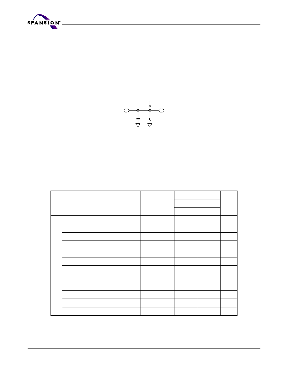
96
S71GL032A Based MCPs
S71GL032A_00_A0 March 31, 2005
A d v a n c e I n f o r m a t i o n
AC Operating Conditions
Test Conditions
Test Load and Test Input/Output Reference
Input pulse level: 0.4 to 2.2V
Input rising and falling time: 5ns
Input and output reference voltage: 1.5V
Output load (See Figure 32): CL= 30pF+1TTL
Notes:
1. Including scope and jig capacitance.
2. R1=3070
, R2=3150
.
3. V
TM
=2.8V.
AC Characteristics
Read/Write Characteristics (V
CC
=2.7-3.3V)
Figure 32. AC Output Load
Parameter List
Symbol
Speed Bins
Units
70ns
Min
Max
Re
a
d
Read cycle time
t
RC
70
-
ns
Address access time
t
AA
-
70
ns
Chip select to output
t
CO1
, t
CO2
-
70
ns
Output enable to valid output
t
OE
-
35
ns
LB#, UB# Access Time
t
BA
-
70
ns
Chip select to low-Z output
t
LZ1
, t
LZ2
10
-
ns
LB#, UB# enable to low-Z output
t
BLZ
10
-
ns
Output enable to low-Z output
t
OLZ
5
-
ns
Chip disable to high-Z output
t
HZ1
, t
HZ2
0
25
ns
UB#, LB# disable to high-Z output
t
BHZ
0
25
ns
Output disable to high-Z output
t
OHZ
0
25
ns
Output hold from address change
t
OH
10
-
ns
VTM (note 3)
R1 (note 2)
CL (note 1)
R2 (note 2)
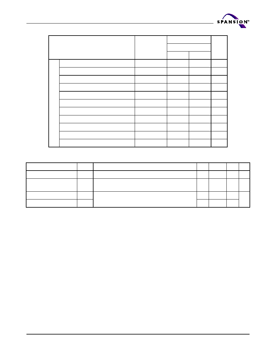
March 31, 2005 S71GL032A_00_A0
S71GL032A Based MCPs
97
A d v a n c e I n f o r m a t i o n
Data Retention Characteristics (4M Version F)
Notes:
1. CS1 controlled:CS1#
V
CC
-0.2V. CS2 controlled: CS2 0.2V.
2. Typical values are not 100% tested.
W
r
ite
Write cycle time
t
WC
70
-
ns
Chip select to end of write
t
CW
60
-
ns
Address set-up time
t
AS
0
-
ns
Address valid to end of write
t
AW
60
-
ns
LB#, UB# valid to end of write
t
BW
60
-
ns
Write pulse width
t
WP
50
-
ns
Write recovery time
t
WR
0
-
ns
Write to output high-Z
t
WHZ
0
20
ns
Data to write time overlap
t
DW
30
-
ns
Data hold from write time
t
DH
0
-
ns
End write to output low-Z
t
OW
5
-
ns
Item
Symbol
Test Condition
Min
Typ
Max Unit
V
CC
for data retention
V
DR
CS1# V
CC
-0.2V (Note 1), V
IN
0V. BYTE# = V
SS
or V
CC
1.5
-
3.3
V
Data retention current
I
DR
V
CC
=3.0V, CS1# V
CC
-0.2V (Note 1), V
IN
0V
-
1.0
(Note 2)
10
µA
Data retention set-up time
t
SDR
See data retention waveform
0
-
-
ns
Recovery time
t
RDR
t
RC
-
-
Parameter List
Symbol
Speed Bins
Units
70ns
Min
Max
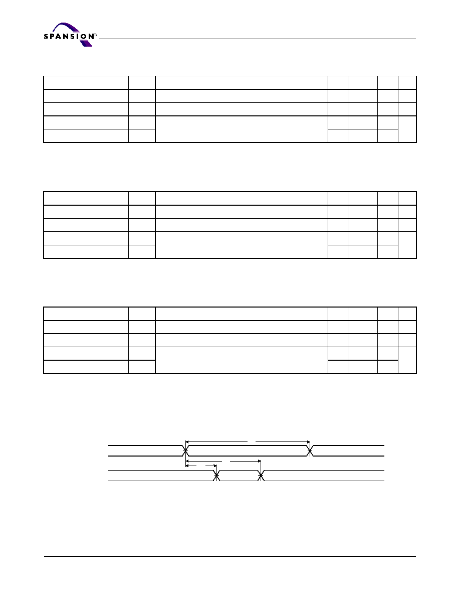
98
S71GL032A Based MCPs
S71GL032A_00_A0 March 31, 2005
A d v a n c e I n f o r m a t i o n
Data Retention Characteristics (4M Version G)
Notes:
1. CS1 controlled:CS1#
V
CC
-0.2V. CS2 controlled: CS2 0.2V.
Data Retention Characteristics (8M Version C)
Notes:
1. CS1 controlled:CS1#
V
CC
-0.2V. CS2 controlled: CS2
0.2V.
Data Retention Characteristics (8M Version D)
Notes:
1. CS1 controlled:CS1#
V
CC
-0.2V. CS2 controlled: CS2
0.2V.
Timing Diagrams
Item
Symbol
Test Condition
Min
Typ
Max Unit
V
CC
for data retention
V
DR
CS1# V
CC
-0.2V (Note 1), V
IN
0V. BYTE# = V
SS
or V
CC
1.5
-
3.3
V
Data retention current
I
DR
V
CC
=1.5V, CS1# V
CC
-0.2V (Note 1), V
IN
0V
-
-
3
µA
Data retention set-up time
t
SDR
See data retention waveform
0
-
-
ns
Recovery time
t
RDR
t
RC
-
-
Item
Symbol
Test Condition
Min
Typ
Max Unit
V
CC
for data retention
V
DR
CS1# V
CC
-0.2V (Note 1). BYTE# = V
SS
or V
CC
1.5
-
3.3
V
Data retention current
I
DR
V
CC
=3.0V, CS1# V
CC
-0.2V (Note 1)
-
-
15
µA
Data retention set-up time
t
SDR
See data retention waveform
0
-
-
ns
Recovery time
t
RDR
t
RC
-
-
Item
Symbol
Test Condition
Min
Typ
Max Unit
V
CC
for data retention
V
DR
CS1# V
CC
-0.2V (Note 1), BYTE# = V
SS
or V
CC
1.5
-
3.3
V
Data retention current
I
DR
V
CC
=3.0V, CS1# V
CC
-0.2V (Note 1)
-
-
TBD
µA
Data retention set-up time
t
SDR
See data retention waveform
0
-
-
ns
Recovery time
t
RDR
t
RC
-
-
Figure 33. Timing Waveform of Read Cycle(1) (Address Controlled, CS#1=OE#=V
IL
, CS2=WE#=V
IH
, UB#
and/or LB#=V
IL
)
t
AA
t
RC
t
OH
Address
Data Out
Previous Data Valid
Data Valid
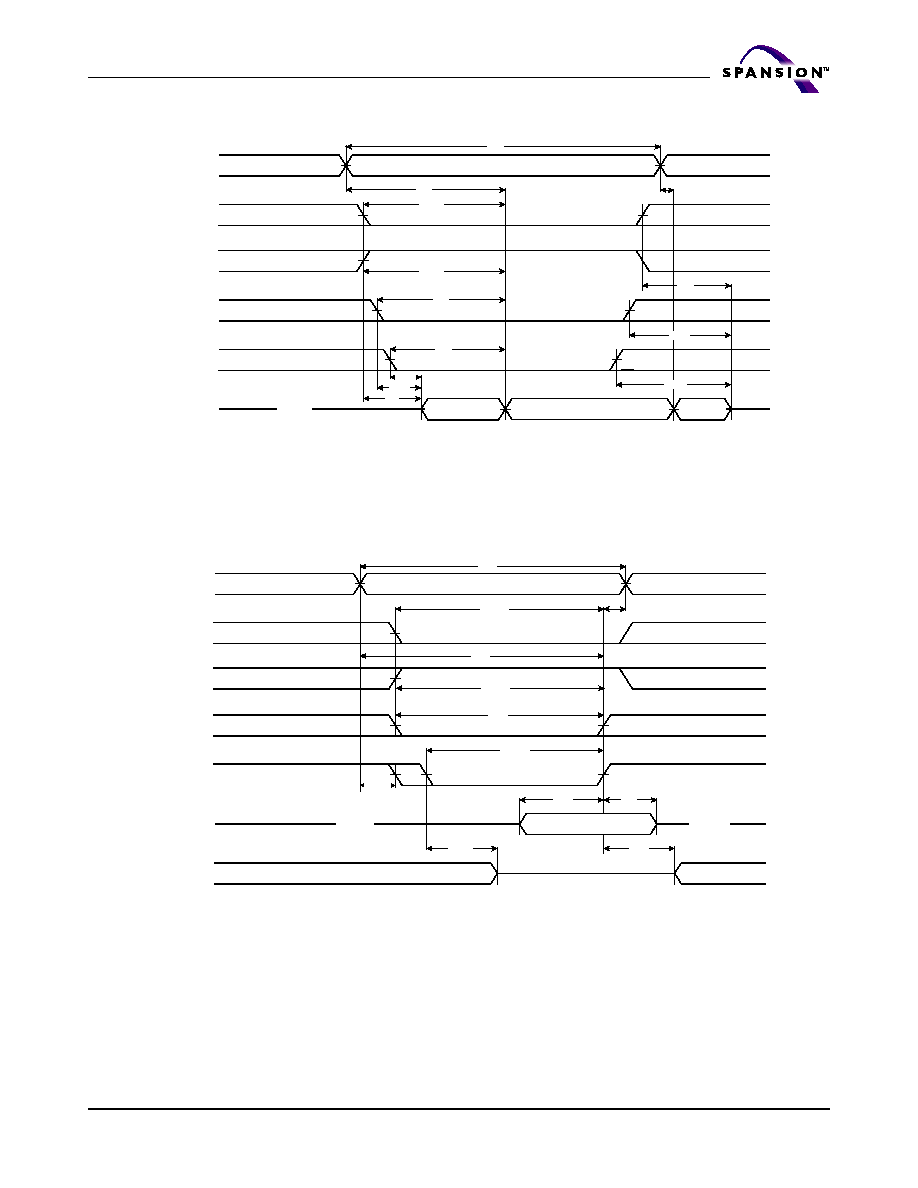
March 31, 2005 S71GL032A_00_A0
S71GL032A Based MCPs
99
A d v a n c e I n f o r m a t i o n
Notes:
1. t
HZ
and t
OHZ
are defined as the time at which the outputs achieve the open circuit conditions and are not referenced to
output voltage levels.
2. At any given temperature and voltage condition, t
HZ
(Max.) is less than t
LZ
(Min.) both for a given device and from
device to device interconnection.
Figure 34. Timing Waveform of Read Cycle(2) (WE#=V
IH
, if BYTE# is Low, Ignore UB#/LB# Timing)
Figure 35. Timing Waveform of Write Cycle(1) (WE# controlled, if BYTE# is Low, Ignore UB#/LB# Timing)
High-Z
t
RC
t
OH
t
AA
t
CO1
t
BA
t
OE
t
OLZ
t
BLZ
t
LZ
t
OHZ
t
BHZ
t
HZ
t
CO2
Address
CS1#
CS2
UB#, LB#
OE#
Data out
Data Valid
t
WC
t
CW(2)
t
WR(4)
t
AW
t
BW
t
WP(1)
t
AS(3)
t
DH
t
DW
t
WHZ
t
OW
High-Z
High-Z
t
CW(2)
Address
CS1#
CS2
UB#, LB#
WE#
Data in
Data out
Data Undefined
Data Valid
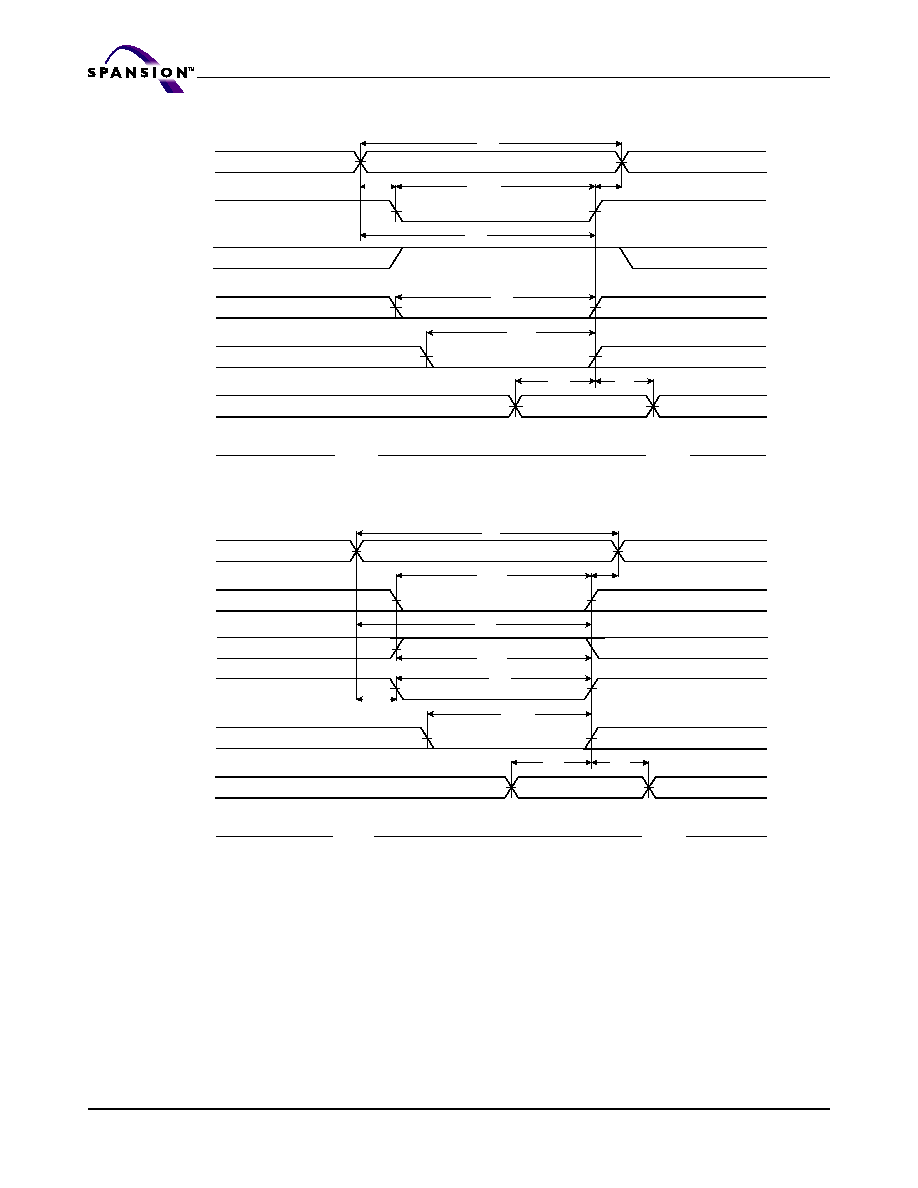
100
S71GL032A Based MCPs
S71GL032A_00_A0 March 31, 2005
A d v a n c e I n f o r m a t i o n
Figure 36. Timing Waveform of Write Cycle(2) (CS# controlled, if BYTE# is Low, Ignore UB#/LB# Timing)
Notes:
1. A write occurs during the overlap (t
WP
) of low CS1# and low WE#. A write begins when CS1# goes low and WE#
goes low with asserting UB# or LB# for single byte operation or simultaneously asserting UB# and LB# for double
byte operation. A write ends at the earliest transition when CS1# goes high and WE# goes high. The t
WP
is
measured from the beginning of write to the end of write.
2. t
CW
is measured from the CS1# going low to the end of write.
3. t
AS
is measured from the address valid to the beginning of write.
4. t
WR
is measured from the end of write to the address change. t
WR
applied in case a write ends as CS1# or WE#
going high.
Figure 37. Timing Waveform of Write Cycle(3) (UB#, LB# controlled)
High-Z
High-Z
t
WC
t
CW(2)
t
AW
t
BW
t
WP(1)
t
DH
t
DW
t
WR(4)
t
AS(3)
Address
CS1#
CS2
UB#, LB#
WE#
Data in
Data out
Data Valid
High-Z
High-Z
t
WC
t
CW(2)
t
BW
t
WP(1)
t
DH
t
DW
t
WR(4)
t
AW
t
AS(3)
t
CW(2)
Address
CS1#
CS2
UB#, LB#
WE#
Data in
Data out
Data Valid
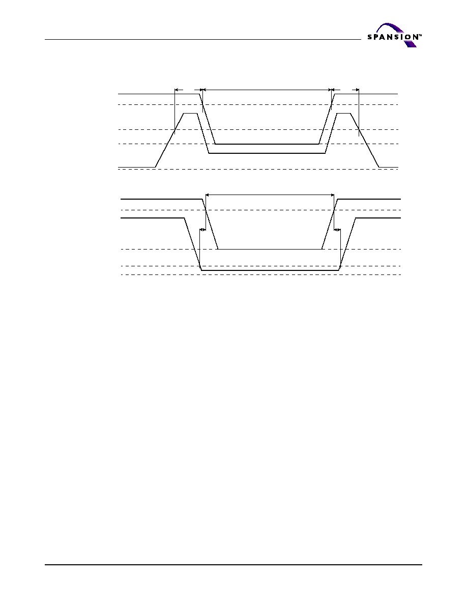
March 31, 2005 S71GL032A_00_A0
S71GL032A Based MCPs
101
A d v a n c e I n f o r m a t i o n
Figure 38. Data Retention Waveform
t
SDR
t
RDR
t
SDR
t
RDR
VCC
2.7V
2.2V
VDR
CS1#
GND
CS1# Controlled
CS2 Controlled
VCC
2.7V
VDR
0.4V
GND
CS2
CS1# VCC - 0.2V
Data Retention Mode
Data Retention Mode
CS2 0.2V

102
S71GL032A Based MCPs
S71GL032A_00_A0 March 31, 2005
A d v a n c e I n f o r m a t i o n
Revision Summary
Revision A (March 31, 2005)
Initial release.
Colophon
The products described in this document are designed, developed and manufactured as contemplated for general use, including without limitation, ordinary
industrial use, general office use, personal use, and household use, but are not designed, developed and manufactured as contemplated (1) for any use that
includes fatal risks or dangers that, unless extremely high safety is secured, could have a serious effect to the public, and could lead directly to death, personal
injury, severe physical damage or other loss (i.e., nuclear reaction control in nuclear facility, aircraft flight control, air traffic control, mass transport control,
medical life support system, missile launch control in weapon system), or (2) for any use where chance of failure is intolerable (i.e., submersible repeater and
artificial satellite). Please note that Spansion will not be liable to you and/or any third party for any claims or damages arising in connection with above-men-
tioned uses of the products. Any semiconductor devices have an inherent chance of failure. You must protect against injury, damage or loss from such failures
by incorporating safety design measures into your facility and equipment such as redundancy, fire protection, and prevention of over-current levels and other
abnormal operating conditions. If any products described in this document represent goods or technologies subject to certain restrictions on export under
the Foreign Exchange and Foreign Trade Law of Japan, the US Export Administration Regulations or the applicable laws of any other country, the prior au-
thorization by the respective government entity will be required for export of those products.
Trademarks and Notice
The contents of this document are subject to change without notice. This document may contain information on a Spansion LLC product under development
by Spansion LLC. Spansion LLC reserves the right to change or discontinue work on any product without notice. The information in this document is provided
as is without warranty or guarantee of any kind as to its accuracy, completeness, operability, fitness for particular purpose, merchantability, non-infringement
of third-party rights, or any other warranty, express, implied, or statutory. Spansion LLC assumes no liability for any damages of any kind arising out of the
use of the information in this document.
Copyright ©2005 Spansion LLC. All rights reserved. Spansion, the Spansion logo, and MirrorBit are trademarks of Spansion LLC. Other company and product
names used in this publication are for identification purposes only and may be trademarks of their respective companies.