 | –≠–ª–µ–∫—Ç—Ä–æ–Ω–Ω—ã–π –∫–æ–º–ø–æ–Ω–µ–Ω—Ç: S111-X | –°–∫–∞—á–∞—Ç—å:  PDF PDF  ZIP ZIP |
S111-X
1 Form A
Solid State Relay
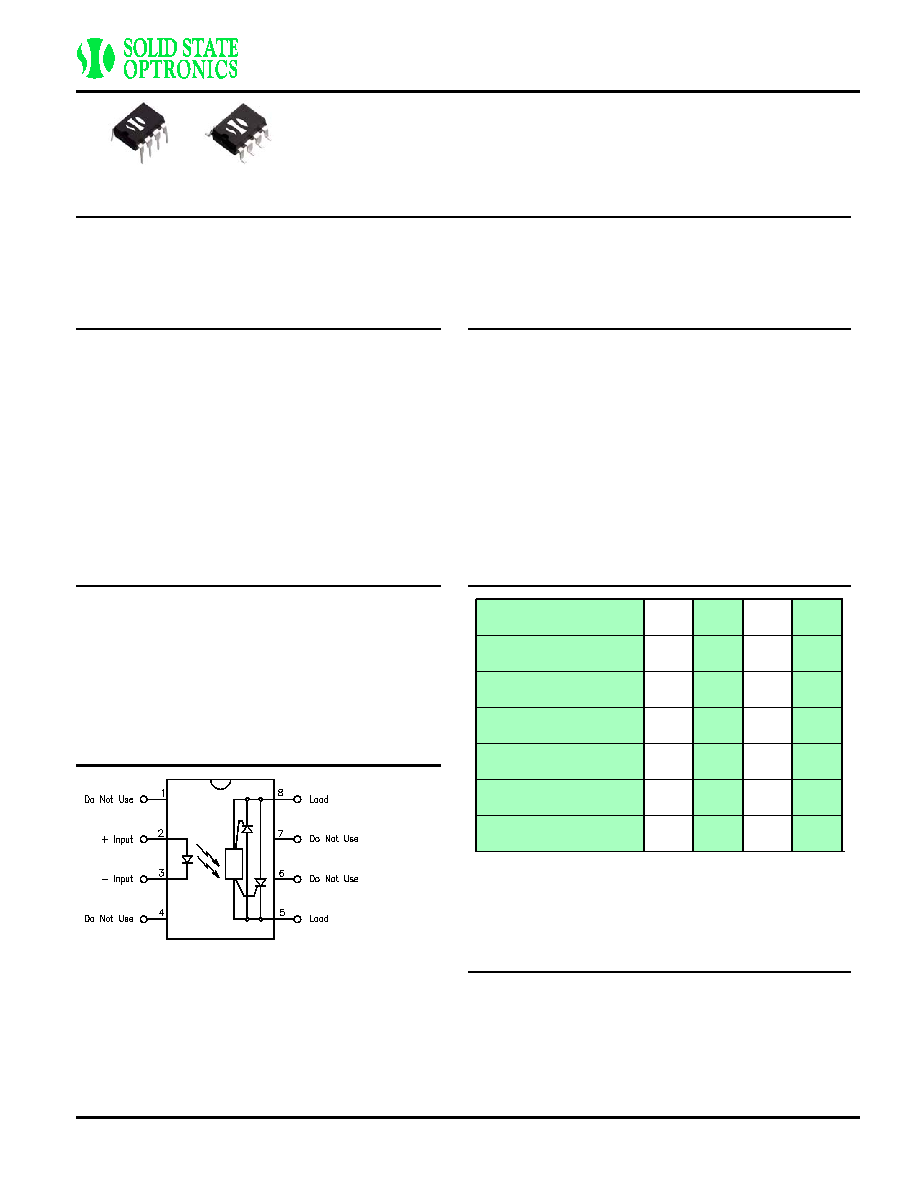
The S111-X is a bi-directional, single-pole, single-throw, normally open multipurpose relay. The circuit is composed of one LED on the
input side which activates an optically coupled IC on the output - controlling the firing angle of two back-to-back SCRs. This circuit
assures no false triggering under most adverse conditions, and a tight zero-volt window not exceeding 5V. A 300-ohm input resistor in
series with the LED is also provided in this circuit.
DESCRIPTION
FEATURES
APPLICATIONS
OPTIONS/SUFFIXES*
SCHEMATIC DIAGRAM
ABSOLUTE MAXIMUM RATINGS*
APPROVALS
Zero-Volt Cross Switching
∑
Internal 300 ohm input resistor
∑
High transient immunity
∑
600V blocking voltage
∑
0.8A maximum continuous current
∑
Low input control current
∑
High input-to-output isolation
∑
Solid state reliability
∑
Valve control
∑
Solenoids
∑
Home appliances
∑
Metering equipment
∑
Heating elements
∑
Gas pump control circuitry
∑
High Output Isolation
∑
-H
Surface Mount Option
∑
-S
Tape and Reel Option
∑
-TR
NOTE: Suffixes listed above are not included in marking on
device for part number identification.
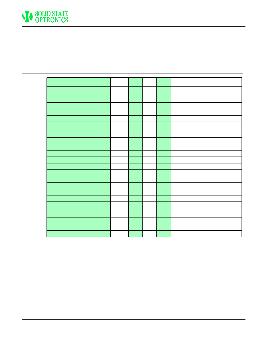
PARAMETER
UNIT
MIN
TYP
MAX
Storage Temperature
∞C
-55
125
Operating Temperature
∞C
-40
85
Continuous Input Current
mA
40
Transient Input Current
mA
400
Reverse Input Control
Voltage
V
6
Output Power Dissipation
mW
800
*The values indicated are absolute stress ratings. Functional operation of the
device is not implied at these or any conditions in excess of those defined in
electrical characteristics section of this document. Exposure to Absolute
Ratings may cause permanent damage to the device and may adversely
affect reliability.
BABT CERTIFICATE #608203:
BS EN 60950, BS EN 41003, BS EN 60065
∑
UL FILE #E90096
∑
© 2004 Solid State Optronics ∑ San JosÈ, CA
www.ssousa.com ∑ +1.408.293.4600
Page 1 of 5
S111-X
rev 1.40 (10/25/2004)
S111-X
1 Form A
Solid State Relay
ELECTRICAL CHARACTERISTICS - 25∞C
PARAMETER
UNIT
MIN
TYP
MAX TEST CONDITIONS
INPUT SPECIFICATIONS
LED Forward Voltage
V
1.2
1.5
If = 10mA
LED Reverse Voltage
V
6
12
Ir = 10uA
Input Resistor
300
Must Operate Current
m
2.5
5
Io = 0.8A, resistive load
A
Junction Capacitance
p
5
Vf = 0V
F
OUTPUT SPECIFICATIONS
Blocking Voltage
V
600
Io = 600uA
Continuous Load Current
A
0.8
If = 5mA
Surge Current Rating
A
10
T = 16ms
Holding Current
m
10
A
On-Voltage
V
1.2
Io = 0.8A
Voltage Across Load at Turn-On
V
5
If = 5mA
Leakage Current
µ
100
250
Vo = 250V
A
Thermal Resistance
∞
120
C /
W
Power Factor
0.3
Critical Rate of Rise (dV/dt)
V
400
/
µ s
COUPLED SPECIFICATIONS
Isolation Voltage
V
2500
T = 1 minute
-H Suffix
V
3750
T = 1 minute
Isolation Resistance
G
100
Coupled Capacitance
p
6
F
© 2004 Solid State Optronics ∑ San JosÈ, CA
www.ssousa.com ∑ +1.408.293.4600
Page 2 of 5
S111-X
rev 1.40 (10/25/2004)
S111-X
1 Form A
Solid State Relay
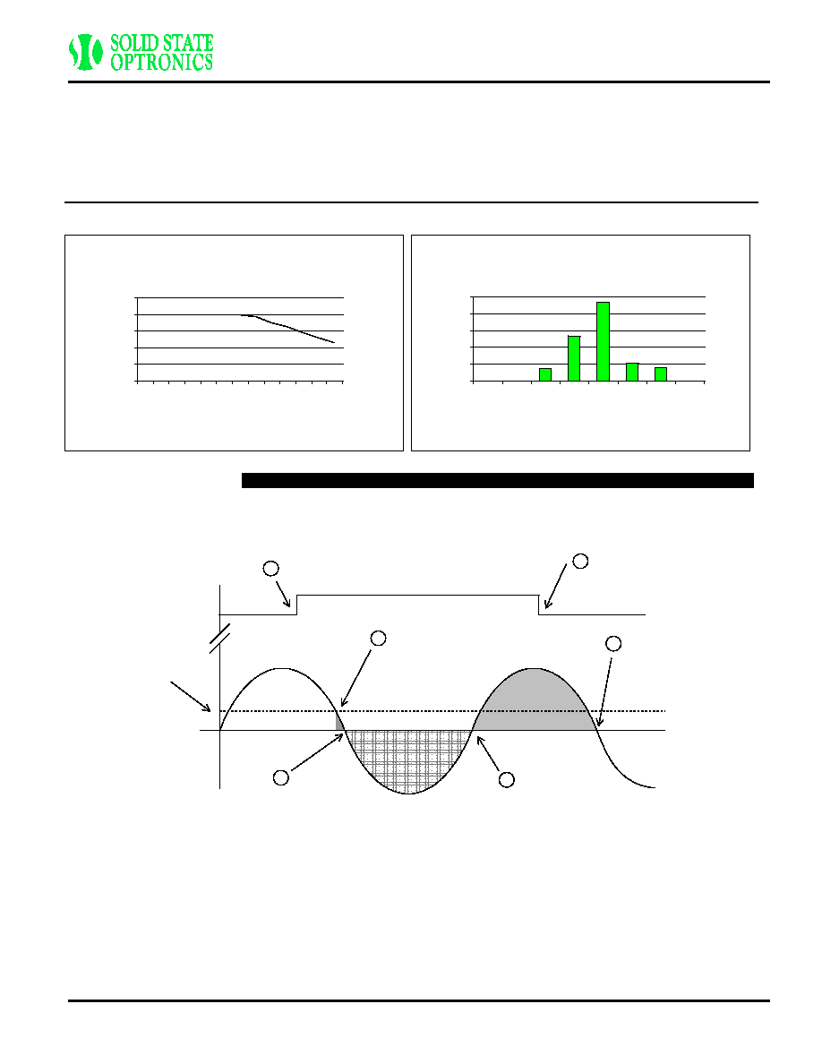
PERFORMANCE DATA
0
10
20
30
40
50
620 630 640 650 660 670 680 690
Blocking Voltage (V)
D
e
v
i
c
e
C
ount
S111-X
Typical Blocking Voltage Distribution
N = 100, Ambient Temperature = 25∞C
0
200
400
600
800
1000
-4
0
-2
0
0
20
40
60
80
Tem perature (C)
Loa
d
C
ur
r
e
nt
(
m
A
)
S111-X
Maximum Load Current vs. Temperature
5 V
Threshold
Input Signal
SCR #1 Turns On when
5V threshold is reached.
SCR #1 Turns Off,
SCR #2 Turns On
at Zero Volts.
SCR #2 Turns Off,
SCR #1 Turns On
at Zero Volts.
SCR #1 and Relay Turn
Off at Zero Volts.
5
4
2
6
3
1
Relay Input Signal is
Turned On.
Relay Input Signal is
Turned Off.
This solid state relay has been designed with a driver circuit that controls the operation of two back-to-back silicon controlled rectifiers
(SCRs), each responsible for one half of the AC cycle. If an AC signal is examined, the turn on, turn off and zero-volt switching can be seen.
Figure 1 shows a typical 60 Hz, 120Vac signal with a corresponding relay input signal:
ZERO-VOLT SWITCHING
Figure 1 shows the sequence of zero-volt switching operation. At Stage 1, an input signal is applied to the relay. The relay will not turn on
until the threshold voltage of 5V is reached. Once this point is reached (Stage 2), SCR #1 (designated as the SCR which controls positive
AC voltage) turns on. However, SCR #1 only conducts for an instant, as the cycle quickly crosses zero. At this point (Stage 3), SCR #1 will
turn off and SCR #2 (negative AC voltage) turns on. Likewise, at the next zero cross (Stage 4), SCR #2 will turn off and SCR #1 conducts
again. Even though the input signal is terminated at Stage 5, the relay will continue to conduct (typical SCR behavior) until Stage 6, when
SCR #1 crosses zero and ceases to conduct. Please note that turn on can likewise begin on the negative phase of the AC cycle with a -5V
threshold, though only the positive phase is shown here.
© 2004 Solid State Optronics ∑ San JosÈ, CA
www.ssousa.com ∑ +1.408.293.4600
Page 3 of 5
S111-X
rev 1.40 (10/25/2004)
S111-X
1 Form A
Solid State Relay
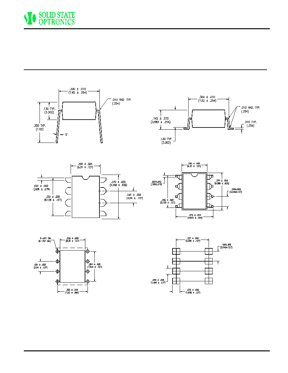
MECHANICAL DIMENSIONS
8 PIN DUAL IN-LINE PACKAGE
8 PIN SURFACE MOUNT DEVICE
END VIEW
END VIEW
TOP VIEW
TOP VIEW
BOTTOM VIEW/
BOARD PATTERN
BOTTOM VIEW/
BOARD PATTERN
© 2004 Solid State Optronics ∑ San JosÈ, CA
www.ssousa.com ∑ +1.408.293.4600
Page 4 of 5
S111-X
rev 1.40 (10/25/2004)
S111-X
1 Form A
Solid State Relay
Solid State Optronics (SSO) makes no warranties or representations with regards to the completeness and accuracy of this document. SSO
reserves the right to make changes to product description, specifications at any time without further notice.
SSO shall not assume any liability arising out of the application or use of any product or circuit described herein. Neither circuit patent
licenses nor indemnity are expressed or implied.
Except as specified in SSO's Standard Terms & Conditions, SSO disclaims liability for consequential or other damage, and we make no other
warranty, expressed or implied, including merchantability and fitness for particular use.
DISCLAIMER
LIFE SUPPORT POLICY
SSO does not authorize use of its devices in life support applications wherein failure or malfunction of a device may lead to personal injury or
death. Users of SSO devices in life support applications assume all risks of such use and agree to indemnify SSO against any and all
damages resulting from such use. Life support devices are defined as devices or systems which, (a) are intended for surgical implant into the
body, or (b) support or sustain life, and (c) whose failure to perform when used properly in accordance with instructions for use can be
reasonably expected to result in significant injury to the user, or (d) a critical component in any component of a life support device or system
whose failure can be reasonably expected to cause failure of the life support device or system, or to affect its safety or effectiveness.
© 2004 Solid State Optronics ∑ San JosÈ, CA
www.ssousa.com ∑ +1.408.293.4600
Page 5 of 5
S111-X
rev 1.40 (10/25/2004)