
SDD451
DC Input
Optocoupler
The SDD451 consists of a photo Darlington transistor optically coupled to a light emitting diode. Optical coupling between the input LED
and output phototransistor allows for high isolation levels while maintaining low-level DC signal control capability. The SDD451 provides an
optically isolated method of controlling many interface applications such as telecommunications, industrial control and instrumentation
circuitry.
DESCRIPTION
FEATURES
APPLICATIONS
OPTIONS/SUFFIXES
SCHEMATIC DIAGRAM
MAXIMUM RATINGS
APPROVALS
High current transfer ratio
(CTR: MIN.600% at If=1mA, Vce=2V)
∑
High input-to-output isolation package (
3750 Vrms)
∑
4 Pin small outline package
∑
System appliances, measuring instruments
∑
Industrial robots
∑
Copiers, automated vending machines
∑
Signal transmission between varying circuits
∑
Telephone sets
∑
Fax machines
∑
Interface with various power supply circuits
∑
Numerical control machines
∑
Tape and Reel
∑
-TR
PARAMETER
UNIT
MIN
TYP
MAX
Storage Temperature
∞C
-40
125
Operating Temperature
∞C
-40
100
Continuous Input Current
mA
50
Transient Input Current
A
1
Reverse Input Control
Voltage
V
6
Output Power Dissipation
mW
170
UL and C-UL approved File#
E201932
∑
rev 1.0
Solid State Optronics, Inc.
1.888.377.4776
www.ssousa.com
52
1. Anode
2. Cathode
3. Emitter
4. Collector
SDD451
DC Input
Optocoupler
ELECTRICAL CHARACTERISTICS - 25∞
PARAMETER
UNIT
MIN
TYP
MAX TEST CONDITIONS
INPUT SPECIFICATIONS
LED Forward Voltage
V
1.2
1.4
If = 20mA
LED Reverse Current
µ
10
VR=4V
A
OUTPUT SPECIFICATIONS
Collector-Emitter Breakdown Voltage
V
35
Emitter-Collector Voltage
V
5
Dark Current
µ
1
Vce = 10V, If=0
A
Floating Capacitance
p
0.6
1
V= 0V, f=1.0MHz
F
Saturation Voltage
V
1
If = 20mA, Ic = 1mA
Current Transfer Ratio
%
600
7500
If = 1mA, Vce = 2V
Rise Time
µ
60
Ic = 2mA, Vc
e = 2V, Rc = 100 ohms
s
Fall Time
µ
5
0
Ic = 2mA, Vc
e = 2V, Rc = 100 ohms
s
COUPLED SPECIFICATIONS
Isolation Voltage
V
5000
T = 1 minute
Isolation Resistance
G
50
Cut off Frequency
k
7
Ic = 2mA, Vcc = 5V, Rc = 100 ohms
H z
rev 1.0
Solid State Optronics, Inc.
1.888.377.4776
www.ssousa.com

SDD451
rev 1.0 Solid State Optronics, Inc.
1.888.377.4776
www.ssousa.com
Fig.2 Collector Power Dissipation vs.
Ambient Temperature
Ambient Temperature Ta (∞C)
Diode power dissipation Pc (mW)
Fig.1 Forward Current vs. Ambient
Temperature
Ambient Temperature Ta (∞C)
Forward Current I
F
(mA)
Fig.3 Peak Forward Current vs. Duty
Ratio
Duty ratio
Peak forward Current I
FM
(mA)
Fig.5 Current Transfer Ratio vs.
Forward Current
Forward Current I
F
(mA)
Current transfer ratio CTR (%)
Fig.6 Collector Current vs. Collector-
emitter Voltage
Collector Current Ic (mA)
Collector current I
C
(mA)
Fig.8 Collector-emitter Saturation
Voltage vs. Ambient Temperature
Ambient Temperature Ta (∞C)
Collector-emitter saturation V
oltage V
CE
(SA
T) (V)
Fig.9 Collector Dark Current vs.
Ambient Temperature
Ambient Temperature Ta (∞C)
Collector dark current I
CEO
(A)
Fig.11 Collector-emitter Saturation
Voltage vs. Forward current
Ambient temperature Ta (∞C)
Collector-emitter saturation voltage V
CE
(sat) (V)
Fig.4 Forward Current vs. Forward
Voltage
Forward voltage V
F
(V)
Forward Current I
F
(mA)
Fig.7 Relative Current Transfer Ratio
vs. Ambient Temperature
Ambient Temperature Ta (∞C)
Relative current transfer ratio (%)
Fig.10 Response Time vs. Load
Resistance
Load resistance R
L
(K ohm)
Response T
ime (us)
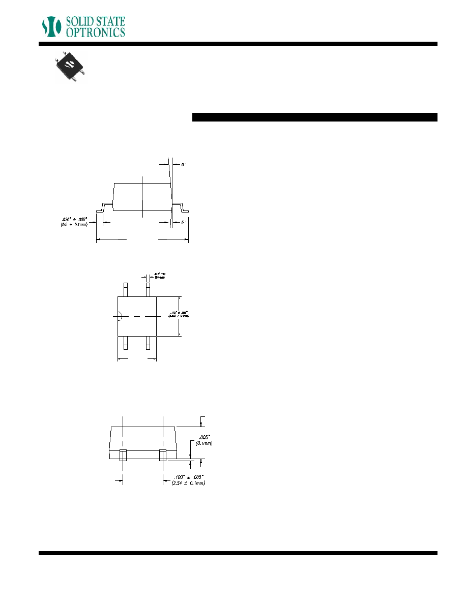
MECHANICAL DIMENSIONS
4 PIN SMALL OUTLINE PACKAGE
rev 1.0
Solid State Optronics, Inc.
1.888.377.4776
www.ssousa.com
END VIEW
TOP VIEW
BACK VIEW
.275" ± 0.015"
(6.985 ± 0.4mm)
.80" ± 0.005"
(1.96 ± 0.13mm)
.170" ± 0.010"
(4.165 ± 0.3mm)
SDD451
DC Input
Optocoupler