 | Электронный компонент: SSSB148 | Скачать:  PDF PDF  ZIP ZIP |
¡ 1 ¡
Swindon Silicon Systems Limited
December 1994
SSSB148
2.5GHz 16:1 Multiplexer
SDH Product Range
The SSSB148 is a very high speed 16 : 1 parallel to serial data converter suitable for digital voice or data communication
applications.
╖
High performance Silicon Bipolar Technology
╖
2.5 GHz minimum clock frequency
╖
ECL100k compatible parallel data inputs
╖
50
differential serial data output
╖
Low jitter contribution
╖
Differential or single ended 2.5 GHz clock input
╖
Single power supply (¡5V)
╖
Low dissipation (800 mW)
╖
44 pin J¡leaded ceramic package
╖
Evaluation board available
2.5GHz 16:1 MULTIPLEXER
FEATURES
APPLICATIONS
╖
High speed instrumentation
╖
Fibre¡optic communication
╖
SDH STM1 to STM16 Multiplexing
╖
Computer to computer interface
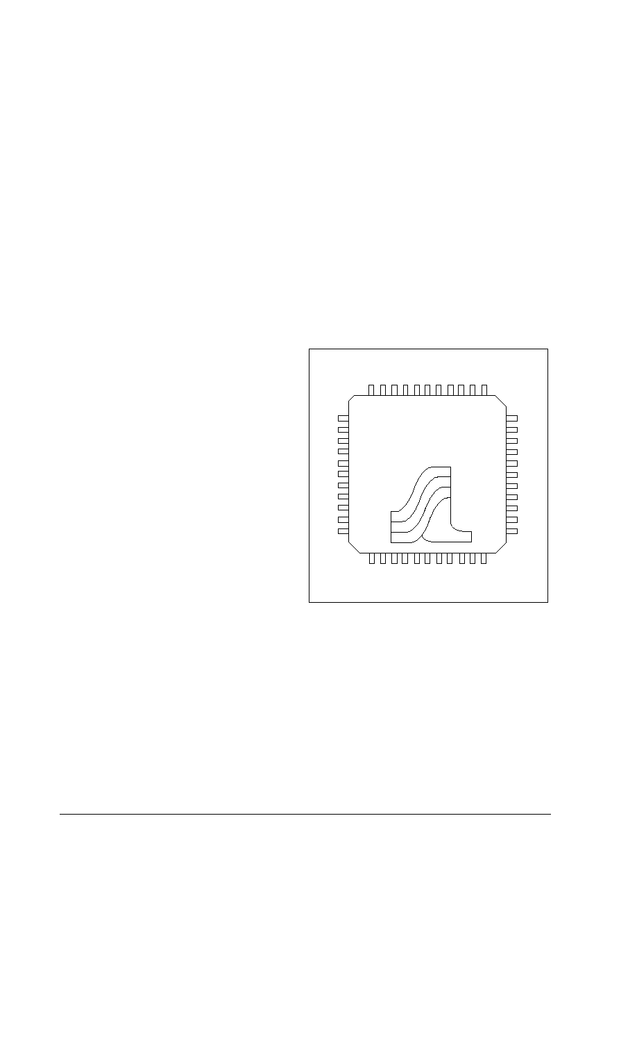
Q
B
Q
B
Q
Q
C
K
C
K
B
D
1
2
D
1
1
D
1
0
D
9
D
8
D
7
D
6
D
5
D
4
D
3
V
CC
REFR
V
CC
TCK
ICK
V
CC
V
EE
D0
D1
D2
V
CC
V
EE
V
CC
SCK
V
CC
V
EE
D15
D14
D13
SSSB148
DATE CODE
SSSB148
2.5GHz 16:1 Multiplexer
¡ 2 ¡
Swindon Silicon Systems Limited
December 1994
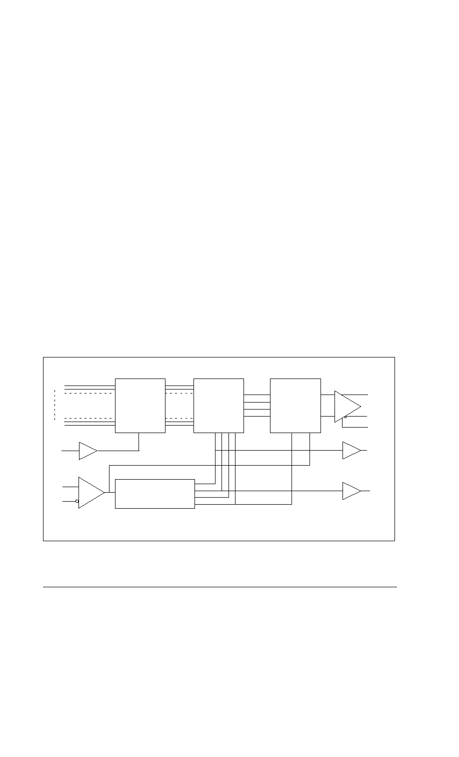
Block Diagram
ICK
REFR
Q
QB
TCK
SCK
TIMING
GENERATOR
CK
CKB
FUNCTIONAL DESCRIPTION
Parallel data is applied to the device as a 16 bit word to the data inputs D15 ¡ D0. Data is clocked into the input registers
on the rising edge of the ICK clock input. The ICK clock signal is not independent of other clocks and must be derived
from the TCK clock output. Data is serialised and re¡timed in the Multiplexer and output register circuits, then fed
through the differential output buffer to Q and QB. The latency of this device depends on process and temperature
variations, and on the external delay from TCK to ICK. Serial data output of each word starts 1/2 to 1 cycle of the TCK
clock after it was clocked into the input registers. Serial data output is in the order D15 first, D0 last.
The 2.5GHz clock is internally divided by 16 to produce the internal clocks and the 155MHz TCK and SCK signals.
These signals have a nominal 50 : 50 mark space ratio. The TCK clock output is designed to be connected directly to
the ICK clock input. The ICK clock signal is fed through the I/O buffers, rather than being connected internally to the
timing generator circuit, to optimise the timing of the external circuits driving the data input register. The SCK clock
output is phase advanced with respect to TCK by 1/4 of the TCK period.
The serial data outputs Q and QB are designed to drive 50
transmission lines externally terminated to V
CC
(ground),
and incorporate on chip 50
resistors for back matching purposes. An external 2k
resistor (and parallel 10nF
decoupling capacitor) must be connected between the REFR pin and V
CC
to set the optimum drive current into the
external 50
load resistors.
The 2.5GHz clock inputs to the device are very versatile, and can accept ECL or high frequency sine wave drive (AC
coupled) from single ended or differential clock sources.
The D15 ¡ D0 and ICK pins are ECL 100k compatible inputs with 50k
pulldown resistors.
The TCK and SCK pins are ECL 100k compatible outputs.
MULTIPLEXER
INPUT
REGISTER
OUTPUT
REGISTER
D15
D0
MULTIPLEXER
SSSB148
2.5GHz 16:1 Multiplexer
¡ 3 ¡
Swindon Silicon Systems Limited
December 1994
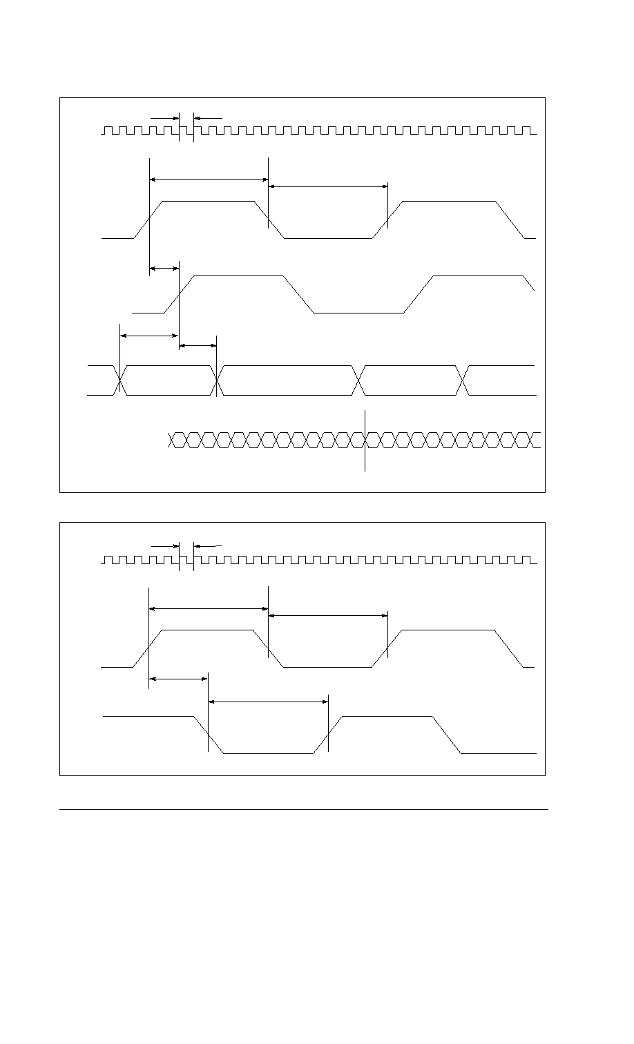
TIMING DIAGRAMS
12
11
10
09
08
07
06
05
04
03
02
01
00
15
14
13
12
04
P
8P
8P
t
dti
t
h
t
s
CK
TCK
ICK
D15¡D0
Q, QB
Word n valid
Word n + 1 valid
Word n
Word n ¡ 1
11
10
09
08
07
06
05
8P
4P
SCK
P
8P
8P
CK
TCK
SSSB148
2.5GHz 16:1 Multiplexer
¡ 4 ¡
Swindon Silicon Systems Limited
December 1994
V
EE
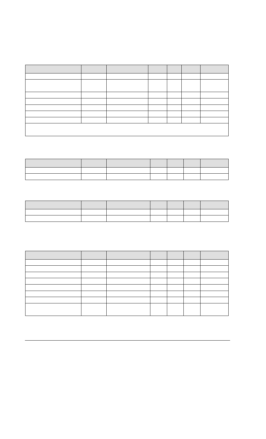
ABSOLUTE MAXIMUM RATINGS
Parameter
Symbol
Min
Max
Units
Conditions
Supply Voltage
V
CC
V
I
V
CC
= 0V
V
Input Voltage D15¡D0,
ICK, CK, CKB
V
Output Current TCK, SCK
I
out
mA
+150
Junction Temperature
T
j
¡6.0
Storage Temperature
¡65
+0.5
Useful life may be impaired if the device is operated outside these limits
Typ
V
EE
40
░
C
T
stg
+150
All pins are protected against ESD. However, the normal ESD precautions for high speed devices must be observed
at all times
V
EE
OPERATING CONDITIONS
Parameter
Symbol
Min
Max
Units
Conditions
Operating Supply Voltage
70
T
a
V
CC
= 0V
V
Ambient Temperature
¡5.5
¡4.5
Typ
No forced air cooling
0
These operating conditions apply to all subsequent characteristics, unless otherwise stated
P
D
GENERAL
Parameter
Symbol
Min
Max
Units
Conditions
Power Dissipation
mW
800
1200
Typ
V
IH
PARALLEL LOAD INPUTS
Parameter
Symbol
Min
Max
Units
Conditions
Input High Level
¡1.475
V
IL
V
Input Low Level
V
Input High Current
I
IH
╡
A
Maximum Input Data Rate
D
IX
¡1.165
Data Setup Time
1.5
¡0.880
Typ
¡1.810
V
IN
= V
IH(Max)
150
MBit/s
t
s
ns
D15 to D0 and ICK
155
Data Hold Time
t
h
1.0
ns
External Delay from TCK
output to ICK input
1.0
ns
ELECTRICAL CHARACTERISTICS
t
dti
░
C
░
C
(ECL100k inputs)
Input Voltage REFR
V
V
I
V
EE
+0.5V
V
CC
Output Voltage Q, QB
V
O
V
CC
¡1.8V
V
CC
Input Low Current
I
IL
╡
A
V
IN
= ¡2V
25
SSSB148
2.5GHz 16:1 Multiplexer
¡ 5 ¡
Swindon Silicon Systems Limited
December 1994
V
OH
Parameter
Symbol
Min
Max
Units
Conditions
Output High Level
V
OL
V
Output Low Level
V
Rise Time
t
rq
ps
Fall Time
t
fq
¡0.02
Jitter Contribution
Typ
¡0.6
200
ps
ps RMS
SERIAL DATA OUTPUTS
Q and QB
These characteristics apply with both outputs terminated with a 50
1% resistor to V
CC,
and with a 2k
1% resistor between REFR and V
CC
.
200
20% to 80%
20% to 80%
10
V
OH
Parameter
Symbol
Min
Max
Units
Conditions
Output High Level
¡1.620
V
OL
V
Output Low Level
V
Rise Time
t
r
ns
Fall Time
t
f
¡1.035
TCK skew
¡0.880
Typ
¡1.810
1.5
ns
ns
SCK skew
ns
LOW SPEED (155MHz) CLOCK OUTPUTS
TCK and SCK
These characteristics apply when the relevant output is terminated by a 50
resistor to ¡2V (V
TT
)
1.5
20% to 80%
20% to 80%
*1
*1
*1 The TCK and SCK clock outputs are generated internally to the SSSB148 in divide by 16 circuits from the high speed clock input.
The nominal position of each edge on the TCK and SCK outputs is shown in the timing diagrams in terms of the period of the high
speed clock input. The exact position of each edge may vary slightly from this nominal position. The parameter specified here defines
the width of a window, centred on the nominal position, inside which each edge must lie.
(ECL100k outputs)
(50
outputs)
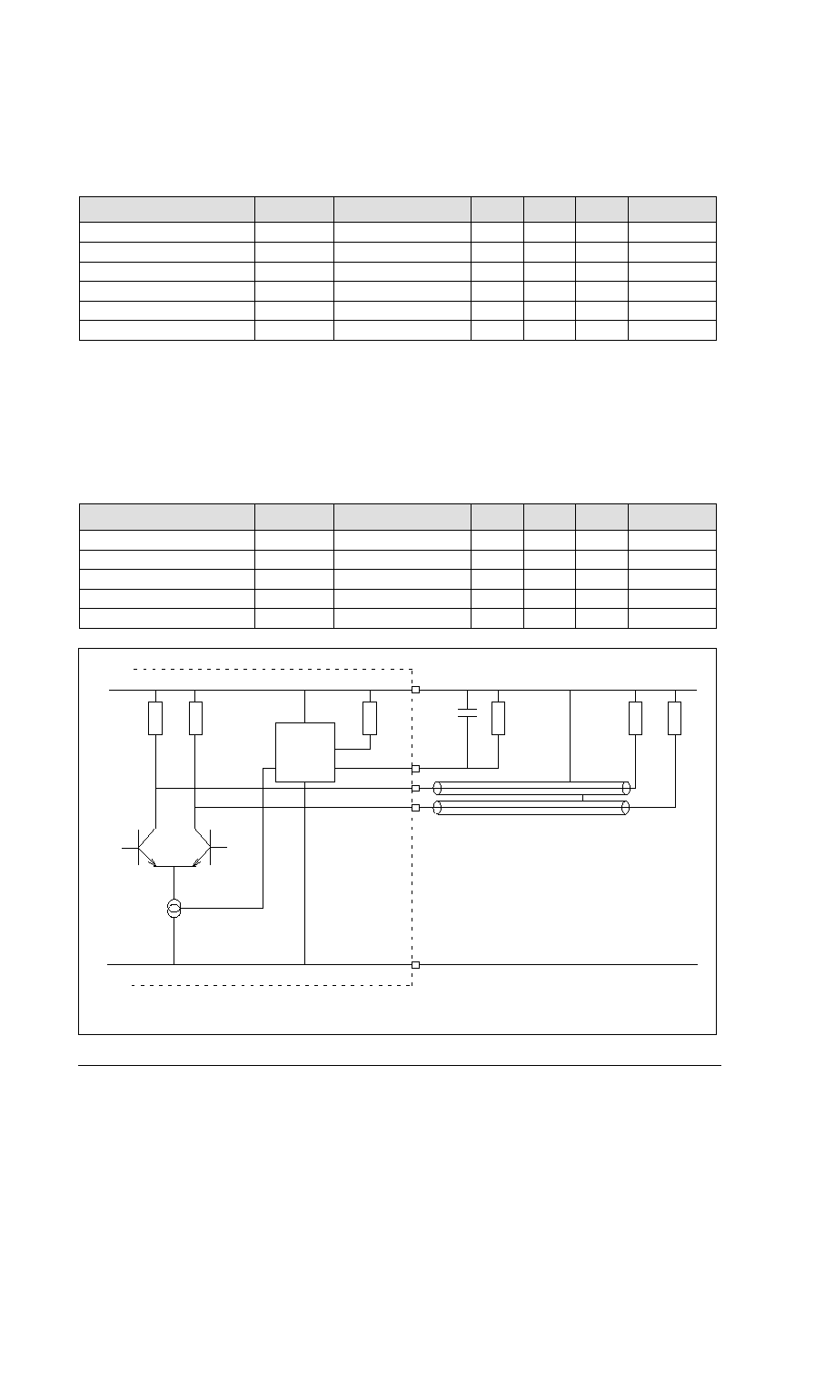
High Speed Data Outputs
Q
QB
V
CC
V
EE
OUTPUT
BIAS
GENERATOR
REFR
50
50
50
50
DEVICE
2k
2k
Unused outputs need not be terminated
0.8
0.8
¡0.54
¡0.66
10nF
SSSB148
2.5GHz 16:1 Multiplexer
¡ 6 ¡
Swindon Silicon Systems Limited
December 1994
F
CK
HIGH SPEED (2.5GHz) CLOCK INPUTS
Parameter
Symbol
Min
Max
Units
Conditions
Maximum Clock Rate
V
slew
GHz
Input Slew Rate
V / ns
Single Ended DC Coupled (ECL 100k) inputs
Minimum Frequency
F
min
2.5
P¡P Amplitude
Typ
0.5
MHz
V
IP
mV
(ECL100k compatible inputs, but internally biased through 1k
to ¡1.32v to allow AC coupling)
100
Single Ended AC Coupled (sine wave) inputs
Input High Level
¡0.88
V
CK and CKB
*2
3.5
*3
200
900
V
IH
Input Low Level
V
IL
600
¡1.55
V
Differential AC Coupled (sine wave) inputs
V
IPP
= |V
CK
¡ V
CKB
|
*2
This device will operate down to zero frequency provided that the minimum input slew rate specification is met.
*3
To ensure correct operation, the clock inputs must always have fast edge speeds. Hence low frequency operation with sine wave
drive is not guaranteed below the minimum sine wave drive frequency specified here.
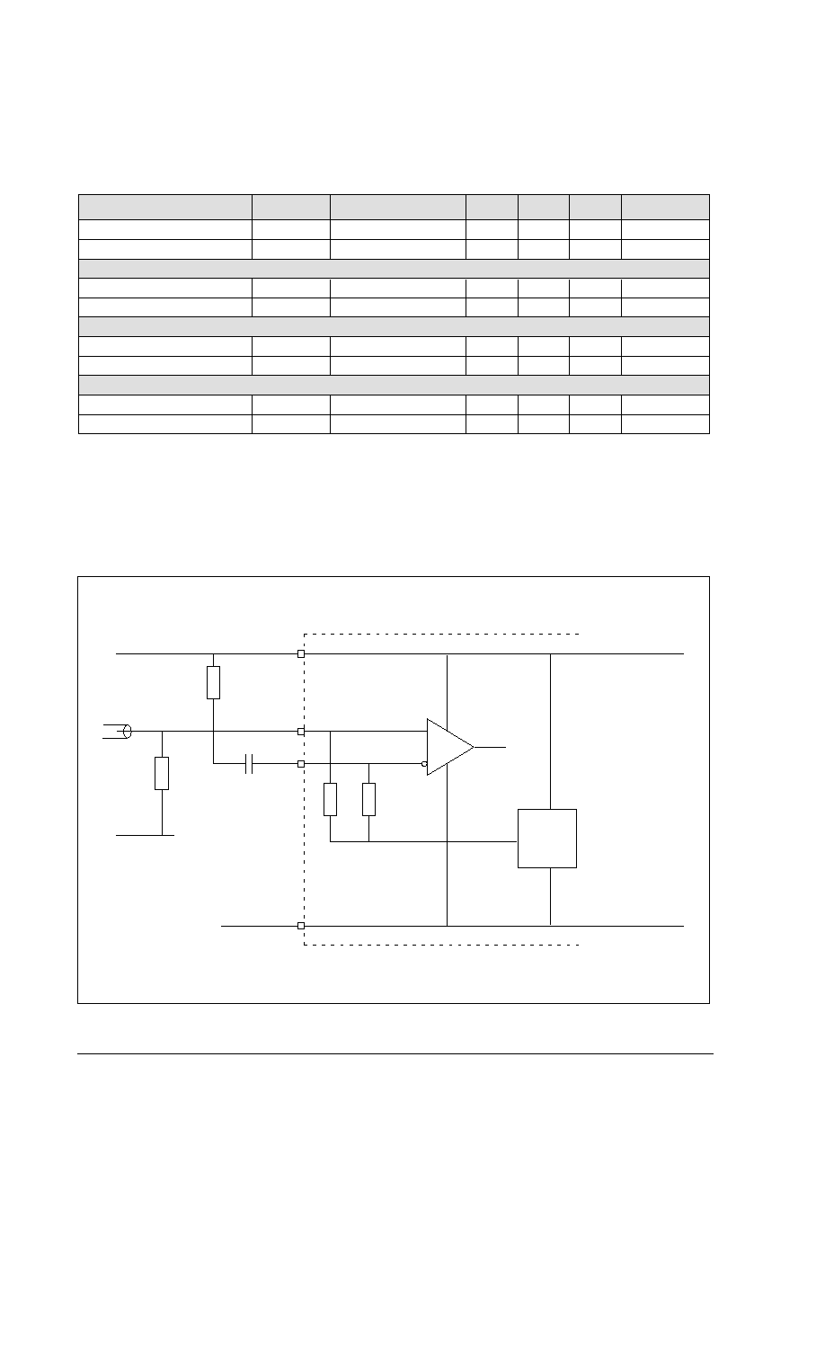
High Speed Clock Inputs
CK
CKB
INPUT
BIAS
GENERATOR
V
CC
V
EE
0V
¡1.32V
¡5V
R
T
DEVICE
Single ended DC coupled (ECL 100k) inputs
1k
1k
¡1.11
¡1.81
Minimum Frequency
F
min
P¡P Amplitude
MHz
V
IPP
mV
100
*3
200
900
400
V
TT
(¡2V)
R
T
SSSB148
2.5GHz 16:1 Multiplexer
¡ 7 ¡
Swindon Silicon Systems Limited
December 1994
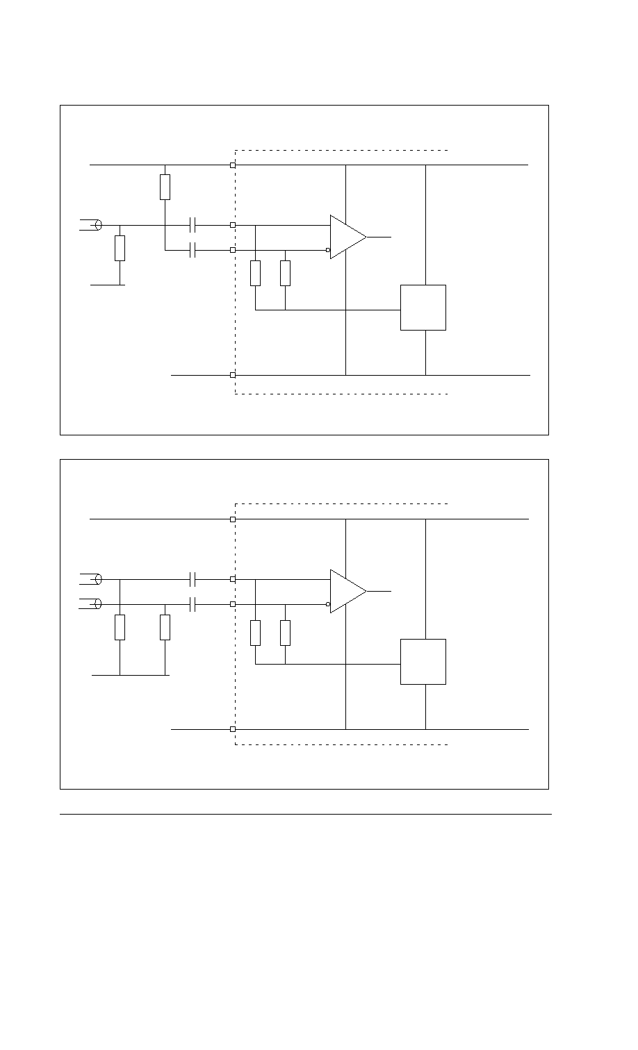
High Speed Clock Inputs
CK
CKB
INPUT
BIAS
GENERATOR
V
CC
V
EE
0V
¡1.32V
¡5V
R
T
DEVICE
High Speed Clock Inputs
CK
CKB
INPUT
BIAS
GENERATOR
V
CC
V
EE
0V
¡1.32V
¡5V
R
T
DEVICE
Single ended AC coupled (sine wave) inputs
V
TT
Differential AC coupled (sine wave) inputs
V
TT
R
T
1k
1k
1k
1k
R
T
SSSB148
2.5GHz 16:1 Multiplexer
¡ 8 ¡
Swindon Silicon Systems Limited
December 1994
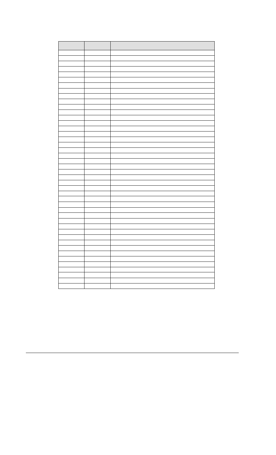
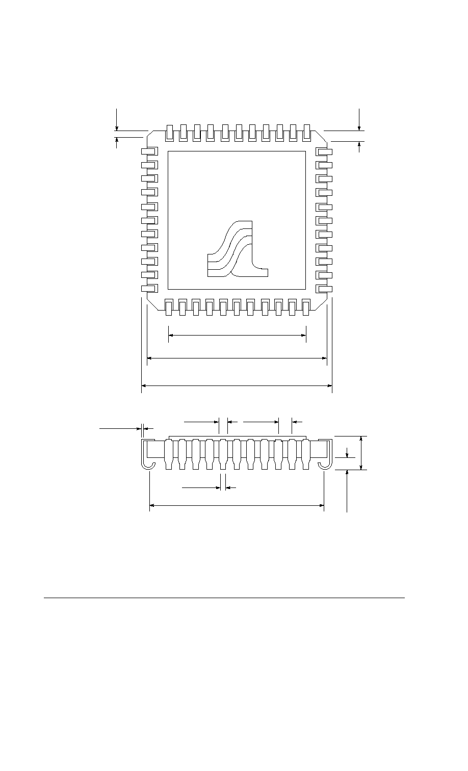
PIN ASSIGNMENT TABLE
Pin No.
Name
Description
1
REFR
Ground
155MHz Clock Output, ECL 100k Compatible
155MHz Clock Output, ECL 100k Compatible
To ensure correct operation :
╖
V
EE
pins (2,21 & 41) and the REFR pin(27) must be decoupled to ground through high speed ceramic capacitors
close to the device pins
╖
For single ended high speed clock inputs, the other input (CK or CKB) must be decoupled to ground through 50
resistors to eliminate the risk of parasitic oscillations.
╖
Pins 34 and 35 must be connected together for the Q output
╖
Pins 37 and 38 must be connected together for the QB output
╖
The Q and QB outputs must have equal loading, even if only one output is in use
╖
Pins 29, 31, 33, 36 & 39 must be No Connection
2
3
4
5
6
7
8
9
10
11
12
13
14
15
16
17
18
19
20
21
22
23
24
25
26
27
28
29
30
31
32
33
34
35
36
37
38
39
40
41
42
43
44
V
CC
V
EE
N/C
D15
D14
D13
D12
D11
D10
D9
D8
N/C
D7
D6
D5
D4
D3
D2
D1
D0
V
EE
V
CC
ICK
N/C
TCK
V
CC
V
CC
N/C
CKB
N/C
CK
N/C
Q
Q
N/C
QB
QB
N/C
V
CC
V
EE
V
CC
SCK
N/C
Negative supply (¡5.0V)
No Connection or Ground
Parallel Data Input (ECL 100k Compatible)
Parallel Data Input (ECL 100k Compatible)
Parallel Data Input (ECL 100k Compatible)
Parallel Data Input (ECL 100k Compatible)
Parallel Data Input (ECL 100k Compatible)
Parallel Data Input (ECL 100k Compatible)
Parallel Data Input (ECL 100k Compatible)
Parallel Data Input (ECL 100k Compatible)
Parallel Data Input (ECL 100k Compatible)
Negative supply (¡5.0V)
Ground
155MHz Clock Input, ECL 100k Compatible
No Connection or Ground
Ground
Output Amplitude Reference Resistor
Ground
Must Be No Connection
2.5GHz Inverted Clock Input
Must Be No Connection
2.5GHz Clock Input
Must Be No Connection
2.5Gbit/S Serial Data Output
2.5Gbit/S Serial Data Output
Must Be No Connection
Inverted 2.5Gbit/S Serial Data Output
Inverted 2.5Gbit/S Serial Data Output
Must Be No Connection
Ground
Negative supply (¡5.0V)
Ground
No Connection or Ground
SSSB148
2.5GHz 16:1 Multiplexer
¡ 9 ¡
Swindon Silicon Systems Limited
December 1994
SSSB148
DATE CODE
Pin 1
40
6
39
29
28
18
17
7
0.500 SQ
0.650 SQ
0.690
▒
0.010
SQ
0.630
▒
0.020
SQ
0.050 typ
0.030 typ
0.017 typ
0.009
+0.002
¡0.001
0.037
▒
0.010
0.040
▒
.010
0.020
▒
.010
PACKAGE DIMENSIONS
44 pin .050 inch pitch
J leaded ceramic chip carrier
Cavity up
╖
Leads are Kovar or Alloy 42
╖
All exposed metal is Gold plated, 60 micro inch minimum over Nickel plated, 100 micro inch minimum
╖
Lid is isolated from all leads
(Top View)
╖
Dimensions are inches
0.115
▒
0.020

SSSB148
2.5GHz 16:1 Multiplexer
¡ 10 ¡
Swindon Silicon Systems Limited
December 1994
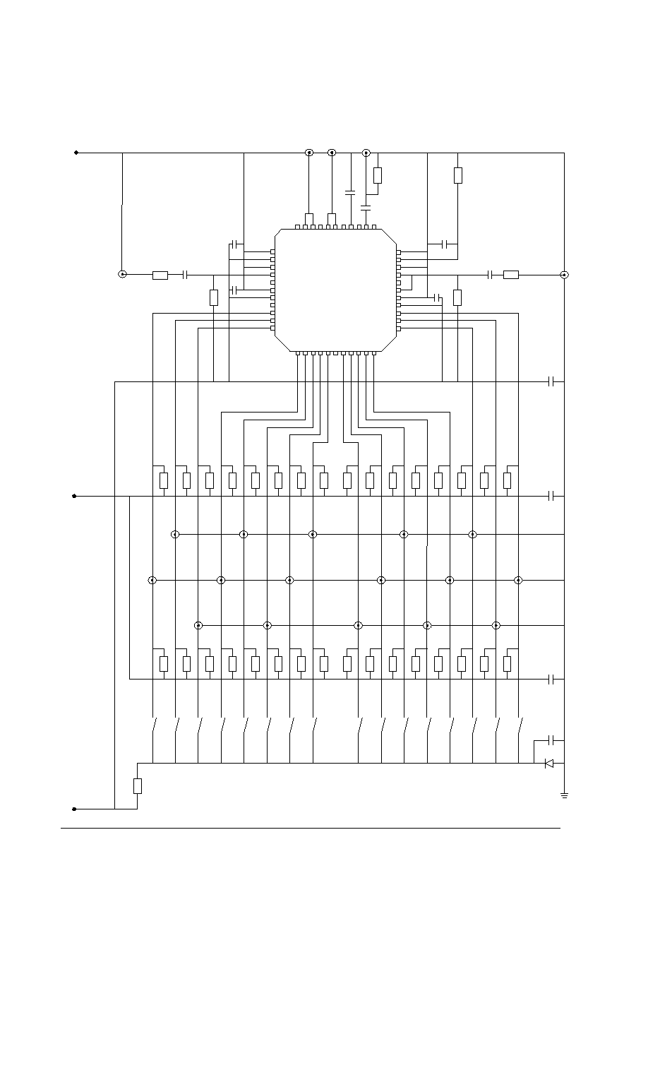
EVALUATION BOARD
An evaluation board for the SSSB148 is available from Swindon Silicon Systems.
This board contains an SSSB148 device and all the necessary supply and signal connections, terminating resistors,
decoupling capacitors, etc. All clock and data signals into and out of the board are through 50
SMA sockets. The
ground plane on the board, and the ground for all the SMA sockets, is the V
CC
supply rail to the SSSB148 device.
The parallel data inputs are provided with a set of DIL switches to force selected inputs high for static drive, and with
a set of 16 SMA sockets for dynamic drive. These parallel data inputs are ECL100k compatible, and have on¡board
terminating resistors of 50
to the ¡2V supply. Data switches must be in the off position for dynamic drive.
The Q and QB high speed data outputs are connected directly to their respective SMA sockets. These outputs are
designed to drive an external load of 50
e.g. the 50
inputs to an oscilloscope. Both outputs must have loads of 50
to V
CC
(GND) for correct operation of the device at full speed. The output level will be around 600mV p¡p into 50
.
Note that on versions of the evaluation board with the SSSB148 in a socket, the output waveforms will be degraded
by the socket inductance, although the board will still operate at full speed.
The device high speed clock inputs are configured for single ended sine wave drive. The clock input to the board, CKB,
has a DC coupled terminating resistor of 50
to V
CC
, and is AC coupled to the SSSB148. The input signal level should
be 0 dBm (1mW into 50
, 632mV p¡p). The operating frequency limits will typically be 100 MHz to 3.5 GHz.
The ICK clock input is connected on the board to the TCK clock output. The TCK and SCK outputs have loads of 130
to the ¡5V supply and are AC coupled to their respective SMA sockets through 50
resistors. This will give a 2 : 1
attenuation into a 50
external load, and so provide around 400mV p¡p to trigger a suitable oscilloscope.
The board requires two power supplies, ¡5V at 300mA and ¡2V at up to 400mA depending on the state of the data
input switches. The connections are GND = 0V, V
TT
= ¡2V and V
EE
= ¡5V.
SSSB148
2.5GHz 16:1 Multiplexer
¡ 11 ¡
Swindon Silicon Systems Limited
December 1994
6
1
40
18
28
39
29
7
17
TCK
SCK
50
50
50
2K
GND
0V
V
TT
¡2V
V
EE
¡5V
SSSB148
(Top View)
D2
D5
D8
D11
D14
D3
D6
D9
D12
D15
D0
D1
D4
D10
D13
D7
S0
S7
S8
S15
Unmarked resistors are 100
Unmarked capacitors are 1nF chip capacitors
QB
Q
CKB
EVALUATION BOARD SCHEMATIC
1nF
1nF
1nF
1nF
IN4145
430
130
130
10nF

SSSB148
2.5GHz 16:1 Multiplexer
¡ 12 ¡
Swindon Silicon Systems Limited December 1994
INTERNATIONAL REPRESENTATIVES / DISTRIBUTORS
HEAD OFFICE
Swindon Silicon Systems
Radnor Street
Swindon
Wiltshire
SN1 3PR
Tel : 01793 614039
Fax : 01793 616215
EUROPE
FRANCE :
Rep Design
5 Rue Carle Vernet
92310 Sevres
Tel : 33¡1¡4623¡7990
Fax : 33¡1¡4623¡7993
ITALY :
Special¡IND
Piazza Spotorno, 3
20159 Milan
Tel : 39¡2¡66805177
Fax : 39¡2¡66800493
FAR EAST
ISRAEL :
IES Ltd
32 Ben-Gurion St
Ramat-Gan 52573
Tel : 972-3-753 0700
Fax : 972-3-753 0701
JAPAN :
Nissho Electronics Corp
3¡1, Tsukiji 7¡chome
Chuo¡ku
Tokyo 104
Tel : 81¡3¡3544¡8495
Fax : 81¡3¡3544¡8280
SOUTH KOREA :
Advance Technology Ltd
Suite 312, Jay 11 B/D
44¡35 Yoido¡dong
Young Deung Po ¡ Ku
Seoul
Tel : 82¡2¡786¡5387
Fax : 82¡2¡786¡5389
This publication is issued to provide outline information only and (unless specifically agreed to the contrary by the company in writing) is
not to be reproduced or to form part of any order or contract or to be regarded as a representation relating to the products or services
concerned. Any applications of product shown in this publication are for illustration purposes only . We reserve the right to alter without notice
the specification, design price or condition of supply of the product.
0000