 | –≠–ª–µ–∫—Ç—Ä–æ–Ω–Ω—ã–π –∫–æ–º–ø–æ–Ω–µ–Ω—Ç: SSSB149 | –°–∫–∞—á–∞—Ç—å:  PDF PDF  ZIP ZIP |
- 1
-
Swindon Silicon Systems Limited
July 2001
SSSB149
2.5GHz 16:1 DeMultiplexer
SDH Product Range
The SSSB149 is a very high speed 16 : 1 serial to parallel data converter suitable for digital voice or data communication
applications. The device incorporates frame recognition and realignment circuitry and complies to ITU-T standards
for SDH.
∑
High performance Silicon Bipolar Technology
∑
2.5 GHz guaranteed clock frequency
∑
ECL100k compatible I/O
∑
Differential or single ended high speed serial
data output
∑
Differential or single ended 2.5 GHz clock input
∑
Single power supply (-5V)
∑
Low dissipation (1300 mW)
∑
44 pin J-leaded ceramic package
∑
Evaluation board available
∑
User programmable or ITU-T A1A2 frame
sync word
2.5GHz 16:1 DEMULTIPLEXER
FEATURES
APPLICATIONS
∑
High speed instrumentation
∑
Fibre-optic communication
∑
Computer to computer interface
D
7
D
8
D
1
5
S
4
B
A
E
N
C
C
K
N
C
VEE
OHW
DIN
N/C
DBIN
TEST
D6
D4
D3
D1
D0
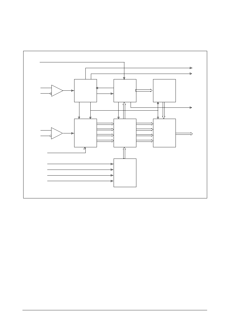
High speed (2.5GBit/s) serial data is applied to the differential inputs (DIN, DBIN) and is clocked into the device by
the 2.5GHz master clock (CK, CKB). The device demultiplexes the serial data into 16 bit words which appear at the
parallel data outputs (D15 - D0). The alignment of the 16 bit output words to the high speed serial data stream is
controlled by internal registers which can be updated by the device when it recognises a synchronisation pattern in the
input data stream. For SDH Telecoms applications, the device is internally programmed for the ITU-T Rec.G708 A1A2
synchronisation pattern. For other applications, the synchronisation pattern can be set by the user. The synchronisation
logic can be disabled to give a fixed relationship between the input data stream and the output word.
FUNCTIONAL OVERVIEW
V
C
C
D
9
D
1
0
D
1
1
D
1
2
D
1
3
D
1
4
F
P
VCC
N/C
VEE
VCC
VCC
VCC
VCC
VCC
C
I
T
T
C
K
B
N
L
O
A
D
L
O
A
D
V
C
C
V
E
E
S
4
D2
D5
VEE
SSSB149
DATE CODE
SSSB149
2.5GHz 16:1 DeMultiplexer
- 2
-
Swindon Silicon Systems Limited
July 2001
BLOCK DIAGRAM
DIN
S4
CK
CKB
SYNCHRO-
NISATION
LOGIC
CLOCK
GENERATOR
ALIGNMENT
REGISTER
D15
-
D0
OHW
SYNC WORD
DETECTOR
SERIAL TO
PARALLEL
CONVERTER
S4B
FP
OUTPUT
FRAMING
SYNC WORD
STORE
DBIN
NCCITT
ENLOAD
A
LOAD
TEST
SSSB149
2.5GHz 16:1 DeMultiplexer
- 3
-
Swindon Silicon Systems Limited
July 2001
FUNCTIONAL DESCRIPTION
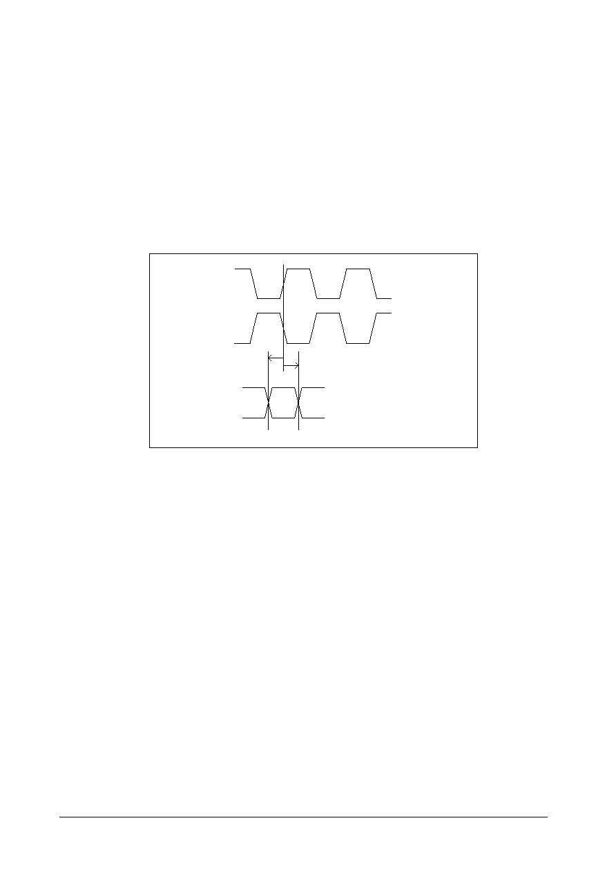
Data is applied to the device as a high speed serial data stream to the differential data inputs, DIN and DBIN. Data is
clocked into the Serial to Parallel converter by the high speed 2.5 GHz differential master clock inputs CK and CKB.
Data is clocked into the device on the rising edge of CK, the falling edge of CKB.
The device has two modes of operation, Synchronisation Mode and Locked Mode depending on the state of the OHW
input. The device is in Synchronisation Mode with OHW at the logic '1' level and in Locked Mode with OHW at the
logic '0'level. In ITU-T applications, OHW is driven to the '1' level to allow device synchronisation, then returned
to zero when synchronisation has occurred. No timing relationships are specified between OHW and the device clock
signals; OHW is assumed to be an asynchronous signal. OHW must be glitch free.
The 2.5 GHz clock and data inputs to the device are very versatile and can accept high frequency sine wave (AC
coupled) or ECL inputs from single ended or differential clock sources. All other inputs and outputs to the device are
ECL100k compatible. To reduce power dissipation, the parallel data outputs are designed to drive a load of 100
to
-2V.
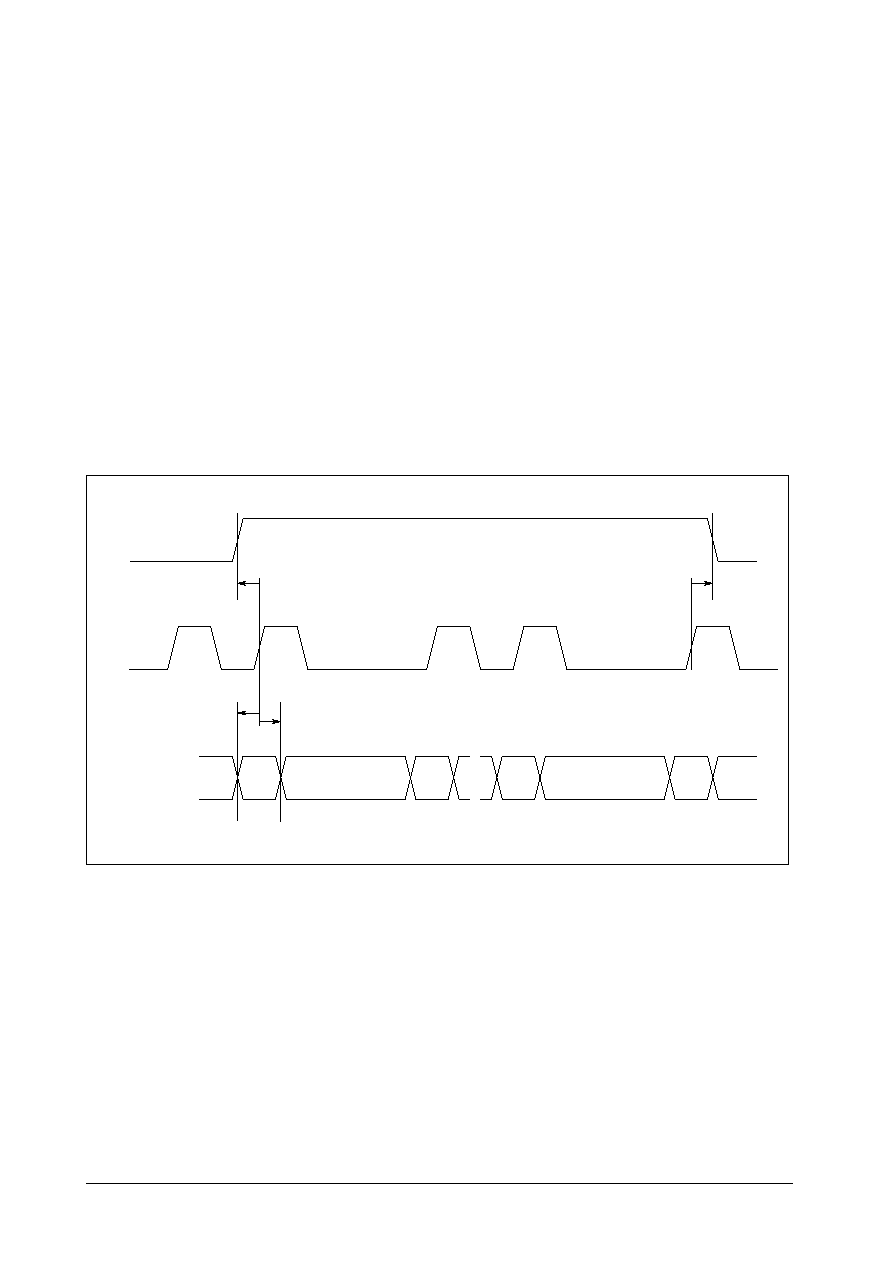
High Speed Input Timing
CK
CKB
DIN
DBIN
t
ds
t
dh
Device synchronisation is achieved by setting a logic "1" (high) on the OHW input. In this mode, the Sync Word
Detector circuit continuously monitors the high speed input data stream until a pattern corresponding to the stored 16
bit sync word is recognised. Upon recognition, the Synchronisation Logic sets the Internal Clock Generator, updates
the output Alignment Register, and produces a Frame Pulse.
The internal Clock Generator produces the internal clocks, and the system clock outputs, S4 and S4B. These clocks
are 1/16 of the input clock frequency, and have a nominal 50 : 50 mark space ratio. The system clock outputs are set
by delaying the next clock edge, thus the width of the clock pulses on the S4 and S4B outputs are never less than 8
times the input clock period.
SSSB149
2.5GHz 16:1 DeMultiplexer
- 4
-
Swindon Silicon Systems Limited
July 2001
The device is locked by setting a logic '0' level (low) on the OHW input. In this mode, re synchronisation will not
occur. The S4 and S4B clock outputs will be a constant 1/16 on the input clock frequency. The alignment of the output
word to the input data stream will be held constant.
In locked mode, frame pulses will be generated whenever the sync word is recognised in the input data stream, even
though the output word may not be aligned to the sync word in the input data stream.
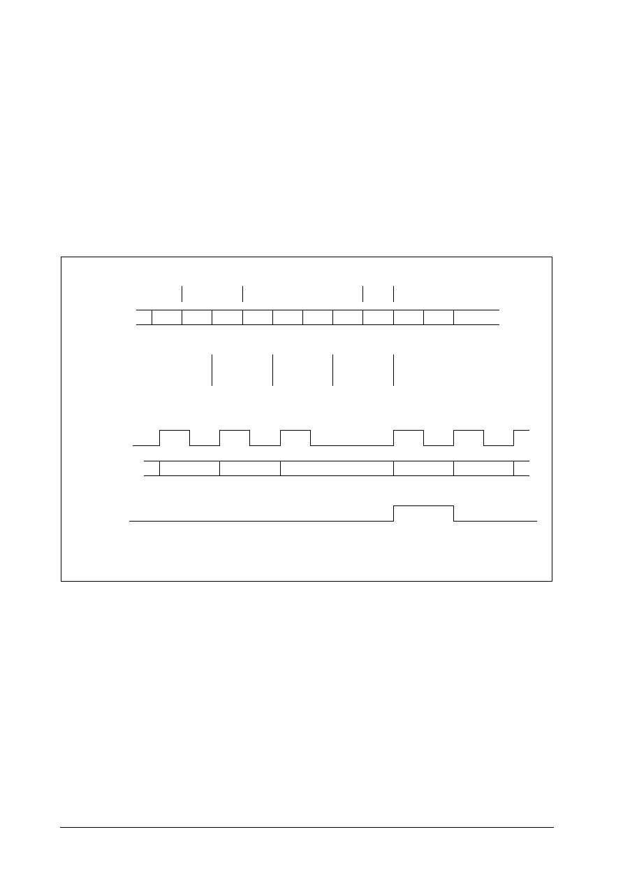
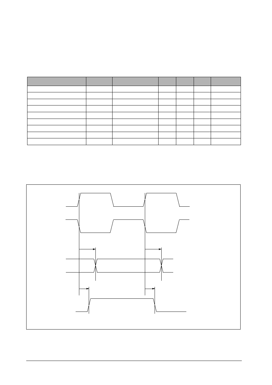
Functional Timing Diagram
Sync Word
1 Byte
or
8 Bits
A1
A1
A2
A2
A2
A2
A2
A2
A2
SERIAL
DATA
STREAM
D15
D0
UT WORD
ING AFTER
HRONISATION
D15
D0 D15
D0
S4B
D15 - D0
FP
Non Valid Data
A2A2
The Alignment Register controls the alignment between the output word and the input data stream. After synchroni-
sation, the output word is aligned to the centre of the sync word. For the first full S4 clock cycle after synchronisation,
the output word, in the order D15 - D0, will be the last 8 bits of the sync word and the next 8 bits in the serial input
data stream. In ITU-T applications, the first output word after synchronisation will be the A2A2 word as shown in
the functional timing diagram below.
The frame pulse output, FP, goes high for the first full S4 cycle after synchronisation. FP is low at all other times.
A2A2
Word 1
Word 2
Word 1
Word 2
SSSB149
2.5GHz 16:1 DeMultiplexer
- 5
-
Swindon Silicon Systems Limited
July 2001
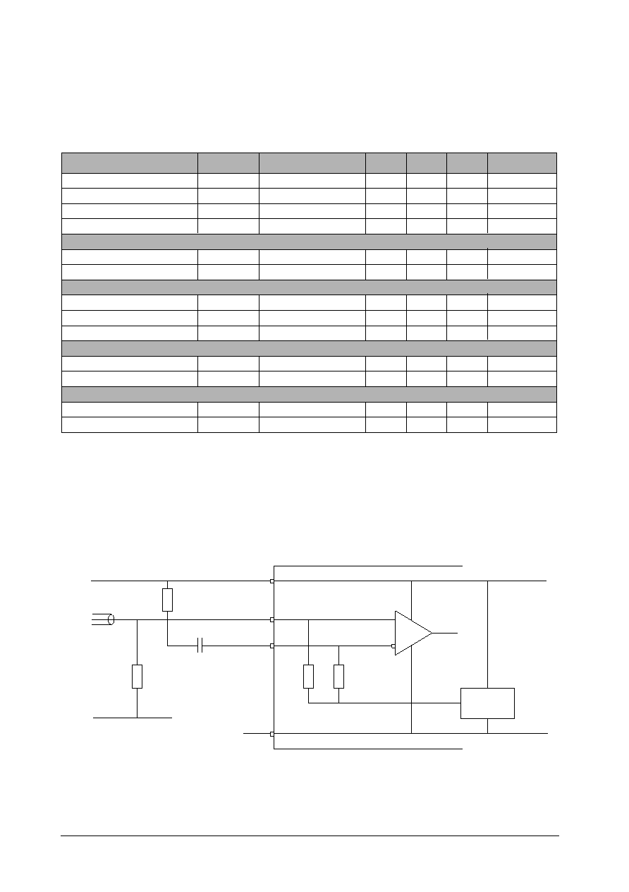
ENLOAD
LOAD
Sync Word Load Timing
15
8
7
0
t
eh
t
es
t
as
t
ah
A
The synchronisation pattern is held in the Sync Word Store. The sync word used to compare with the input data
stream is either a pre-programmed sync word, or the contents of a sync word register, depending on the state of the
NCCITT input.
In ITU-T application, the NCCITT input is held at the logic '0' level (low). With NCCITT = 0, the input data stream
is compared with the pre-programmed A1A2 word as described in ITU-T Rec.G708. This word has the value F628,
and is designed to allow the device to recognise the alignment point as the change in the data stream from a sequence
of repeated bytes with the value F6 (A1) to repeated bytes with the value 28 (A2). The output word will then align
with the first 2828 sequence.
For other applications, NCCITT is held at the logic '1' level (high). With NCCITT = 1, the input data stream is
compared with the contents of the sync word register. The contents of this register are controlled by the A, LOAD
and ENLOAD inputs to the device. The register is serially loaded with data from the A input on rising edges on the
low speed (2MHz) LOAD clock input. New data is loaded in the order bit15 first, bit0 last. ENLOAD must be held
at the logic '1' level (high) to enable new data to be loaded into the register, and returned to zero to enable the new
data to replace the old data as the synchronisation pattern used to compare against the input data stream.
The device has a built in self test facility. For normal device operation, the TEST input must be driven low (or left
open circuit). To enable the device test facility, TEST must be driven high. With the TEST input high, the data input
register is configured as a 5 bit pseudo random pattern generator. If the sync word register is loaded with a pattern
which matches part of the pseudo random sequence, a high 'hit rate' in the sync word detection circuit can be achieved,
and all the internal registers can be tested.

SSSB149
2.5GHz 16:1 DeMultiplexer
- 6
-
Swindon Silicon Systems Limited
July 2001
V
EE
ABSOLUTE MAXIMUM RATINGS
Parameter
Symbol
Min
Ma
Units
Condition
Supply Voltage
V
CC
V
I
V
CC
= 0V
V
Input Voltage
V
Output Current
I
OU
mA
Junction Temperature
T
j
-6.0
Storage Temperature
-55
+0.5
Useful life may be impaired if the device is operated outside these limits
Typ
V
EE
40
∞
C
T
stg
+15
All pins are protected against ESD. However, the normal ESD precautions for high speed devices must be observed at
all times
V
EE
OPERATING CONDITIONS
Parameter
Symbol
Min
Max
Units
Conditions
Operating Supply Voltage
70
T
a
V
CC
= 0V
V
Ambient Temperature
-5.5
-4.5
Typ
No forced air cooling
0
These operating conditions apply to all subsequent characteristics, unless otherwise stated
P
D
GENERAL
Parameter
Symbol
Min
Max
Units
Conditions
Power Dissipation
mW
2200
Typ
V
IH
LOW SPEED INPUTS
Parameter
Symbol
Min
Max
Units
Conditions
Input High Level
-1.475
V
IL
V
Input Low Level
V
Input High Current
I
IH
µ
A
LOAD Clock Rate
F
LOA
-1.165
Data Setup Time
10
-0.88
Typ
-1.81
V
IN
= V
IH(Max)
150
MHz
t
as
ns
OHW, A, LOAD, ENLOAD and TEST
Data Hold Time
t
ah
10
ns
Enable Setup Time
ns
ELECTRICAL CHARACTERISTICS
t
es
∞
C
∞
C
(ECL100k inputs with 50k
pulldown resistors
)
Input Low Current
I
IL
µ
A
V
IN
= -2V
25
2
10
A to LOAD
A to LOAD
ENLOAD to LOAD
10
Enable Hold Time
ns
t
eh
ENLOAD to LOAD
10
+150
SSSB149
2.5GHz 16:1 DeMultiplexer
- 7
-
Swindon Silicon Systems Limited
July 2001
S4B
S4
Output Timing
D15 - D0
FP
t
do
t
do
t
fo
t
fo
V
OH
Parameter
Symbol
Min
Max
Units
Conditions
Output High Level
-1.62
V
OL
V
Output Low Level
V
Rise Time
t
r
ns
Fall Time
t
f
-1.025
Data Offset
-0.88
Typ
-1.81
1.5
ns
ns
Frame Pulse Offset
ns
OUTPUTS
D15 -D0, S4, S4B and FP
These characteristics apply when the relevant output is terminated by a 100
1% resistor to -2V (V
TT
) for the data outputs, and
50
1% to -2V for the S4, S4B and FP outputs
1.5
20% - 80%
20% - 80%
(ECL100k outputs)
0.6
0.6
t
do
-0.3
1.0
t
fo
-0.4
0.6
Duty Cycle S4 & S4B
45
55
%
V
OH
Output High Level
-1.62
V
OL
V
Output Low Level
V
-1.025
-0.88
-1.81
D15 - D0
D15 - D0
S4, S4B and FP
S4, S4B and FP
at -1.3V
at -1.3V
at -1.3V
SSSB149
2.5GHz 16:1 DeMultiplexer
- 8
-
Swindon Silicon Systems Limited
July 2001
F
CK
HIGH SPEED (2.5GHz) CLOCK AND DATA INPUTS
Parameter
Symbol
Min
Max
Units
Conditions
Maximum Clock Rate
V
sle
GHz
Input Slew Rate
V / ns
Single Ended DC coupled (ECL100k) inputs
Minimum Frequency
2.5
P-P Amplitude
Typ
0.5
ps
V
IP
(ECL100k compatible inputs, but internally biased through 1k
to -1.32v to allow AC coupling)
100
Input High Level
-0.88
V
CK, CKB, DIN and DBIN
*2
3.3
V
IH
-1.11
Input Low Level
V
IL
-1.81
-1.55
V
Differential DC coupled inputs
Input High Level
-0.88
V
V
IH
Input Low Level
V
IL
-1.81
V
Input Differential
V
DIF
400
mV
900
*2
This device will operate down to zero frequency provided that the minimum input slew rate specification is met.
*3
To ensure correct operation, the clock inputs must always have fast edge speeds. Hence low frequency operation with sine
wave drive is not guaranteed below the minimum sine wave drive frequency specified here.
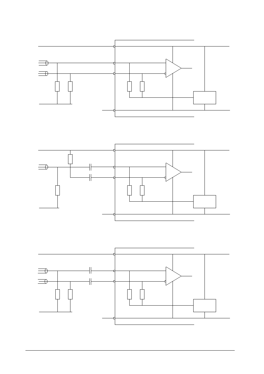
CK
CKB
INPUT
BIAS
GENERATOR
V
CC
V
EE
0V
-1.32V
-5V
R
T
DEVICE
Single Ended DC Coupled (ECL100k) Drive
V
TT
R
T
1k
1k
Data Setup
Data Hold
t
d
ps
t
dh
100
Single Ended AC coupled (Sine wave) inputs
200
MHz
F
min
100
600
900
mV
*3
Minimum Frequency
P-P Amplitude
V
IP
Differential AC coupled (Sine wave) inputs
200
MHz
F
min
100
400
900
mV
*3
HIGH SPEED CLOCK AND DATA INPUT CONFIGURATIONS
SSSB149
2.5GHz 16:1 DeMultiplexer
- 9
-
Swindon Silicon Systems Limited
July 2001
CK
CKB
INPUT
BIAS
GENERATOR
V
CC
V
EE
0V
-1.32V
-5V
R
T
DEVICE
Differential AC Coupled Drive
V
TT
R
T
1k
1k
CK
CKB
INPUT
BIAS
GENERATOR
V
CC
V
EE
0V
-1.32V
-5V
R
T
DEVICE
Single Ended AC Coupled Drive
V
TT
R
T
1k
1k
CK
CKB
INPUT
BIAS
GENERATOR
V
CC
V
EE
0V
-1.32V
-5V
R
T
DEVICE
Differential DC Coupled Drive
V
TT
R
T
1k
1k
-2V

SSSB149
2.5GHz 16:1 DeMultiplexer
- 10
-
Swindon Silicon Systems Limited
July 2001
PIN ASSIGNMENT TABLE
Pin No.
Name
Description
1
Parallel Data Output
Synchronisation Enable Input
To ensure correct operation :
∑
V
EE
pins (9,19, 26 and 42) must be decoupled to ground through high frequency ceramic capacitors close
to the device pins
∑
For single ended high speed clock inputs, the other input (CK or CKB) must be decoupled to ground
through 50
resistors to eliminate the risk of parasitic oscillations
∑
For single ended high speed data inputs, the other input (DIN or DBIN) must be decoupled to ground
through 50
resistors to eliminate the risk of parasitic oscillations
2
3
4
5
6
7
8
9
10
11
12
13
14
15
16
17
18
19
20
21
22
23
24
25
26
27
28
29
30
31
32
33
34
35
36
37
38
39
40
41
42
43
44
D4
D3
N/C
D1
D0
S4
S4B
LOAD
NCCITT
D2
TEST
V
EE
N/C
OHW
V
CC
FP
CKB
CK
D7
V
CC
V
CC
Parallel Data Output
System Clock (155MHz) Output
Negative Supply (-5.0V)
Sync Word Serial Data Input
ITU-T Sync Word Enable (active low)
Test Mode Enable Input
No Connection
Ground
Frame Pulse Output
Ground
Ground
Parallel Data Output
Parallel Data Output
Parallel Data Output
V
CC
Ground
Inverse System Clock (155MHz) Output
V
EE
V
CC
Ground
A
Sync Word Clock Input
ENLOAD
Sync Word Enable Input
Inverse High Speed Clock Input
High Speed Clock Input
V
CC
Ground
Negative Supply (-5.0V)
DBIN
Inverse High Speed Data Input
N/C
No Connection
DIN
High Speed Data Input
No Connection
V
EE
Negative Supply (-5.0V)
V
CC
Ground
D15
Parallel Data Output
D14
D13
D12
D11
D10
D9
D8
Parallel Data Output
Parallel Data Output
Parallel Data Output
Parallel Data Output
Parallel Data Output
Parallel Data Output
Parallel Data Output
Parallel Data Output
V
CC
Ground
V
EE
Negative supply (-5.0V)
D5
D6
Parallel Data Output
Parallel Data Output
SSSB149
2.5GHz 16:1 DeMultiplexer
- 11
-
Swindon Silicon Systems Limited
July 2001
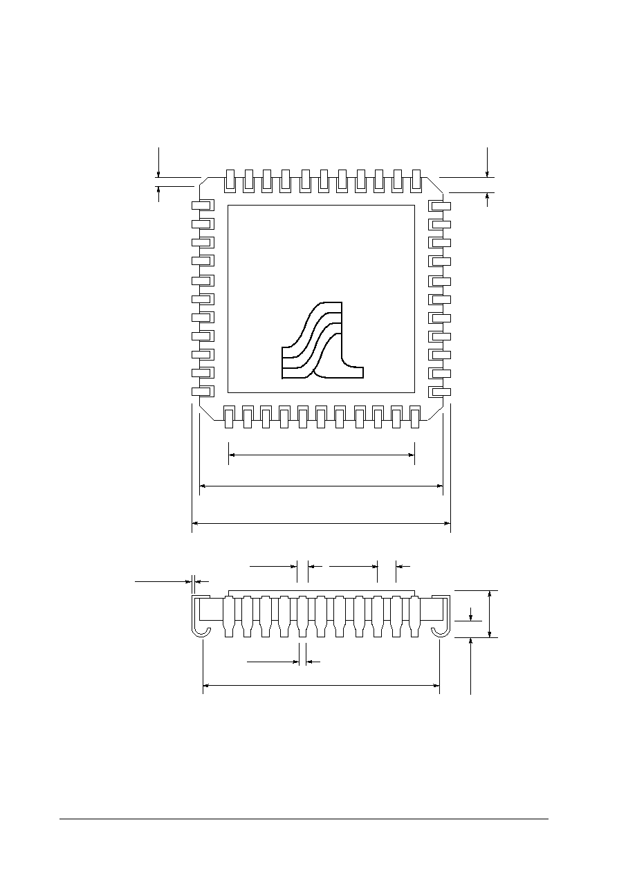
SSSB149
DATE CODE
Pin 1
40
6
39
29
28
18
17
7
0.500 SQ
0.650 SQ
0.690
±
0.010
SQ
0.630
±
0.020
SQ
0.050 typ
0.030 typ
0.017 typ
0.009
+0.002
-0.001
0.037
±
0.010
0.040
±
.010
0.020
±
.010
PACKAGE DIMENSIONS
44 pin .050 inch pitch
J leaded ceramic chip carrier
Cavity up
∑
Leads are Kovar or Alloy 42
∑
All exposed metal is Gold plated, 60 micro inch minimum
over Nickel plated, 100 micro inch minimum
∑
Lid is isolated from all leads
0.115
±
0.020

SSSB149
2.5GHz 16:1 DeMultiplexer
- 12
-
Swindon Silicon Systems Limited
July 2001
EVALUATION BOARD
An evaluation board for the SSSB149 is available from Swindon Silicon Systems.
This board contains an SSSB149 device and all the necessary supply and signal connections, terminating resistors,
decoupling capacitors, etc. The board also includes a divider circuit on the data outputs to provide a suitable trigger
signal for an oscilloscope when running the device self test. All clock and most data signals into and out of the board
are through 50
SMA sockets. The ground plane on the board and the ground for all the SMA sockets is the V
CC
rail to the SSSB149 device.
Inputs
The board requires a power supply of -5V at 600mA (Typ).
The device high speed clock inputs are configured for single ended sine wave drive. The CKIN clock input to the
board should be driven with a signal level of 0dBm (1mW into 50
, 632mVp-p). The operating frequency will
typically be 100MHz to 3.3GHz. This input has a DC coupled terminating resistor of 50
to V
CC
(Ground) and is
AC coupled to the SSSB149 CK input.
The device high speed data inputs are configured for DC coupled differential drive. The board includes switches to
allow data to be input to the device manually. The DIN and DBIN high speed data inputs to the board should be
driven with ECL 100k levels. Both inputs have termination equivalent to 50
to -2V fitted on the board. When the
SMA data input sockets are being driven, the ENDS switch must be off. To allow manual data to be input to the
device from the DIN switch, the ENDS switch must be on and the SMA data input sockets must have no external drive.
The LOAD input to the board is a terminal pin and an SMA socket connected in parallel to the LOAD input of the
device. This input to the board should be driven with ECL 100k levels. This input has a 51
resistor to GND fitted
on the board.
The A input to the board is a terminal pin connected directly to the A input of the device.
The ENLD input to the board is a terminal pin connected through a 1k
resistor to the ENLOAD input of the device.
The A and ENLD inputs to the board should be driven with ECL 100k levels. Note that these inputs do not include
termination resistors, so if ECL devices are used to drive these inputs, external load resistors will be necessary to
ensure correct operation.
The OHW, NCCITT and TEST inputs to the device are driven from switches on the evaluation board. These inputs
have no provision for being driven by external signals.

SSSB149
2.5GHz 16:1 DeMultiplexer
- 13
-
Swindon Silicon Systems Limited
July 2001
Outputs
The 16 parallel data outputs D15 - D0 and the frame pulse output FP have 430
load resistors to -5V and 240
series resistors to their respective SMA sockets. This gives DC coupled 6:1 attenuation into 50
loads. Output signal
levels should be around 140mVp-p into 50
.
The S4 and S4B system clock outputs have 130
load resistors to -5V and AC coupled 51
series resistors to their
respective SMA sockets. This gives AC coupled 2:1 attenuation into 50
loads. Output signal levels should be
around 400mVp-p into 50
.
Operation
If correctly timed clock and data signals can be provided, the device can be operated as described in the functional
operation section of the SSSB149 data sheet. Set the TEST switch to position B, and the ENDS switch to position B.
For incoming data containing the ITU-T A1A2 word '11110110 00101000', put NCCITT to position B. A frame
pulse will occur on the FP output whenever the word is recognised. With OHW in position A, the device will
synchronise on the word each time it occurs, a frame pulse will occur and the '00101000' pattern will appear on
outputs D15 to D8.
With NCCITT in position A, the device will recognise the pattern in the sync word register. The sync word register
is loaded through the A, LOAD and ENLD inputs as described on page 5.

SSSB149
2.5GHz 16:1 DeMultiplexer
- 14
-
Swindon Silicon Systems Limited
July 2001
Self Test Operation
To avoid the need to provide suitably timed high speed data and clock waveforms, the device has a built in self test
facility. With TEST in position A, the data input register is configured as a 5 bit pseudo random pattern generator
with a 31 bit sequence length. If the sync word register is loaded with a pattern which matches part of the pseudo
random sequence, a high 'hit rate' in the sync word detection circuit can be achieved and all the internal registers
can be tested.
To enable the TEST facility, put ENDS to position A, and DIN to position A. With a continuous clock input to the
board CKIN socket, put TEST to position B to initialise the input register, then put TEST to position A to start the
pseudo random sequence. If CKIN is interrupted, or if the maximum or minimum frequency limits are exceeded, the
pseudo random counter can lock up in the all '1' state. The counter can be restarted by setting TEST to B, then back
to A. This lock-up condition only affects the test mode of operation, where the input register is configured as a pseudo
random pattern generation and does not affect normal operation of the device when using the high speed data inputs.
For recognition and synchronisation to occur, the sync word register must be loaded with a section of the pseudo
random sequence. Put NCCITT to position A, and load the word '01111011 01001100' through the A, LOAD and
ENLD inputs as described on page 5.
With OHW in position B and TEST in position A, the device will be in locked mode and will generate a pseudo
random data stream. A frame pulse will occur once every 32 master clock periods. Since one cycle of the S4 clock
and hence the width of the frame pulse is 16 clock cycles, the FP output will have a 50:50 mark space ratio. The
pseudo random sequence is 31 bits long. The pattern on each of the 16 bit parallel data outputs will repeat every 31
cycles of the S4 system clock or 496 cycles of the input master clock. Each of the parallel data outputs will change
state 16 times during the 31 bit sequence. The output of a divide by eight circuit connected to one output (D15) will
have one complete cycle for each 31 bit sequence, so this output (D15/8) can be used as an oscilloscope trigger for
observing the device behaviour.
With TEST in position A and OHW in position A, the device will resynchronise with the pseudo random sequence
to produce a sequence on the parallel data and frame pulse outputs which repeats every 124 master clock cycles. The
D15/8 output does not provide a suitable scope trigger in this mode.

SSSB149
2.5GHz 16:1 DeMultiplexer
- 15
-
Swindon Silicon Systems Limited
July 2001
6
1
40
18
28
39
29
7
17
SSSB149
(Top View)
EVALUATION BOARD SCHEMATIC
10n
10n
10n
10n
GND
8
1
3
13
16
MC
10136
100
D15/
D8
D9
D10 D11 D12 D13 D14 D15
FP
368
10n
-5V
GND
91
91
DIN
DBIN
130
130
-5V
1K
1K
1K
1K
ENDS
DIN
TEST
OHW
NCCITT
-5V
LOAD
GND
GND
GND
A
ENLD
GND
CKIN
S4B
10n
10n
51
51
130
130
-5V
GND
D0
D1
D2
D3
D4
D5
D6
D7
240
430
240
430
240
430
240
430
10n
51
10n
1K
A
B
A
A
A
A
B
B
B
B
S4
51

SSSB149
2.5GHz 16:1 DeMultiplexer
- 16
-
Swindon Silicon Systems Limited
July 2001
INTERNATIONAL REPRESENTATIVES / DISTRIBUTORS
HEAD OFFICE
Swindon Silicon Systems
Radnor Street
Swindon
Wiltshire
SN1 3PR
Tel
: 01793 614039
Fax
: 01793 616215
EUROPE
FRANCE :
Rep Design
5 Rue Carle Vernet
92310 Sevres
Tel
: 33-1-4623-7990
Fax
: 33-1-4623-7993
GERMANY :
Intercomp
Schustergasse 35
55278 Kongernheim
Tel
: 49-6737-9881
Fax
: 49-6737-9882
GERMANY :
Intercomp
Am Hochwald 42
D-8130 Starnberg
Tel
: 49-8151-16044
Fax
: 49-8151-79270
ITALY :
Special-IND
Piazza Spotorno, 3
20159 Milan
Tel
: 39-2-66805177
Fax
: 39-2-66800493
FAR EAST
ISRAEL :
El-Gev Electronics
Building 101
POB 50
Tirat Yehuda
73175
Tel
: 972-3-9712056
Fax
: 972-3-9712407
JAPAN :
Nissho Electronics Corp
3-1, Tsukiji 7-chome
Chuo-ku
Tokyo 104
Tel
: 81-3-3544-8495
Fax
: 81-3-3544-8280
SOUTH KOREA :
Advance Technology Ltd
Suite 312, Jay 11 B/D
44-35 Yoido-dong
Young Deung Po - Ku
Seoul
Tel
: 82-2-786-5387
Fax
: 82-2-786-5389
This publication is issued to provide outline information only and (unless specifically agreed to the contrary by the company in writing)
is not to be reproduced or to form part of any order or contract or to be regarded as a representation relating to the products or services
concerned. Any applications of product shown in this publication are for illustration purposes only. We reserve the right to alter without
notice the specification, design price or condition of supply of the product.