This document contains information on a product under development at FASL LLC. The information is intended to help you evaluate this product. FASL LLC reserves the
right to change or discontinue work on this proposed product without notice.
Publication Number S29JL032H Revision A Amendment 0 Issue Date May 21, 2004
ADVANCE INFORMATION
S29JL032H
32 Megabit (4 M x 8-Bit/2 M x 16-Bit)
CMOS 3.0 Volt-only, Simultaneous Read/Write
Flash Memory
Distinctive Characteristics
Architectural Advantages
Simultaneous Read/Write operations
-- Data can be continuously read from one bank while
executing erase/program functions in another bank.
-- Zero latency between read and write operations
Multiple Bank architecture
-- Four bank architectures available (refer to Table
2
).
Boot Sectors
-- Top and bottom boot sectors in the same device
-- Any combination of sectors can be erased
Manufactured on 0.13 µm process technology
SecSiTM (Secured Silicon) Sector: Extra 256 Byte
sector
-- Factory locked and identifiable: 16 bytes available for
secure, random factory Electronic Serial Number;
verifiable as factory locked through autoselect
function.
-- Customer lockable: One-time programmable only.
Once locked, data cannot be changed
Zero Power Operation
-- Sophisticated power management circuits reduce
power consumed during inactive periods to nearly
zero.
Compatible with JEDEC standards
-- Pinout and software compatible with single-power-
supply flash standard
Package options
48-pin TSOP
Performance Characteristics
High performance
-- Access time as fast as 55 ns
-- Program time: 4 µs/word typical using accelerated
programming function
Ultra low power consumption (typical values)
-- 2 mA active read current at 1 MHz
-- 10 mA active read current at 5 MHz
-- 200 nA in standby or automatic sleep mode
Cycling Endurance: 1 million cycles per sector
typical
Data Retention: 20 years typical
Software Features
Supports Common Flash Memory Interface (CFI)
Erase Suspend/Erase Resume
-- Suspends erase operations to read data from, or
program data to, a sector that is not being erased,
then resumes the erase operation.
Data# Polling and Toggle Bits
-- Provides a software method of detecting the status of
program or erase cycles
Unlock Bypass Program command
-- Reduces overall programming time when issuing
multiple program command sequences
Hardware Features
Ready/Busy# output (RY/BY#)
-- Hardware method for detecting program or erase
cycle completion
Hardware reset pin (RESET#)
-- Hardware method of resetting the internal state
machine to the read mode
WP#/ACC input pin
-- Write protect (WP#) function protects the two
outermost boot sectors regardless of sector protect
status
-- Acceleration (ACC) function accelerates program
timing
Sector protection
-- Hardware method to prevent any program or erase
operation within a sector
-- Temporary Sector Unprotect allows changing data in
protected sectors in-system

2
S29JL032H
S29JL032HA0 May 21, 2004
A D V A N C E I N F O R M A T I O N
General Description
The S29JL032H is a 32 megabit, 3.0 volt-only flash memory device, organized as
2,097,152 words of 16 bits each or 4,194,304 bytes of 8 bits each. Word mode
data appears on DQ15≠DQ0; byte mode data appears on DQ7≠DQ0. The device
is designed to be programmed in-system with the standard 3.0 volt V
CC
supply,
and can also be programmed in standard EPROM programmers.
The device is available with an access time of 55, 60, 70, or 90 ns and is offered
in a 48-pin TSOP package. Standard control pins--chip enable (CE#), write en-
able (WE#), and output enable (OE#)--control normal read and write operations,
and avoid bus contention issues.
The device requires only a single 3.0 volt power supply for both read and write
functions. Internally generated and regulated voltages are provided for the pro-
gram and erase operations.
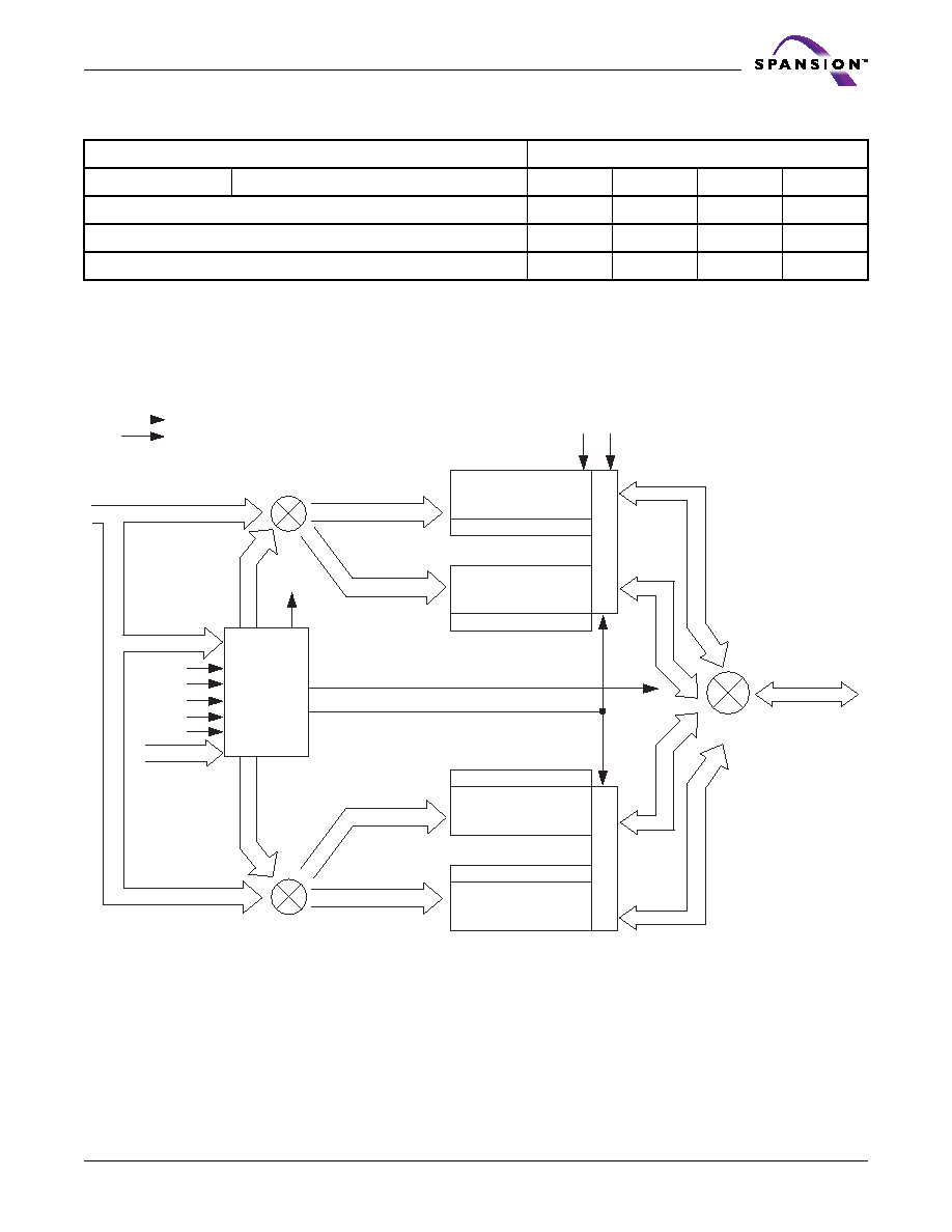
Simultaneous Read/Write Operations with Zero Latency
The Simultaneous Read/Write architecture provides simultaneous operation
by dividing the memory space into separate banks (see Table
2
). Sector ad-
dresses are fixed, system software can be used to form user-defined bank
groups.
During an Erase/Program operation, any of the non-busy banks may be read
from. Note that only two banks can operate simultaneously. The device can im-
prove overall system performance by allowing a host system to program or erase
in one bank, then immediately and simultaneously read from the other bank, with
zero latency. This releases the system from waiting for the completion of program
or erase operations.
The S29JL032H can be organized as both a top and bottom boot sector
configuration.
S29JL032H Features
The SecSiTM (Secured Silicon) Sector is an extra 256 byte sector capable of
being permanently locked by FASL or customers. The SecSi Customer Indicator
Bit (DQ6) is permanently set to 1 if the part has been customer locked, perma-
nently set to 0 if the part has been factory locked, and is 0 if customer lockable.
This way, customer lockable parts can never be used to replace a factory locked
part.
Factory locked parts provide several options. The SecSi Sector may store a se-
cure, random 16 byte ESN (Electronic Serial Number), customer code
(programmed through Spansion programming services), or both. Customer Lock-
able parts may utilize the SecSi Sector as bonus space, reading and writing like
any other flash sector, or may permanently lock their own code there.
DMS (Data Management Software) allows systems to easily take advantage
of the advanced architecture of the simultaneous read/write product line by al-
lowing removal of EEPROM devices. DMS will also allow the system software to
be simplified, as it will perform all functions necessary to modify data in file struc-
tures, as opposed to single-byte modifications. To write or update a particular
piece of data (a phone number or configuration data, for example), the user only
needs to state which piece of data is to be updated, and where the updated data
is located in the system. This is an advantage compared to systems where user-
written software must keep track of the old data location, status, logical to phys-
ical translation of the data onto the Flash memory device (or memory devices),

May 21, 2004 S29JL032HA0
S29JL032H
3
A D V A N C E I N F O R M A T I O N
and more. Using DMS, user-written software does not need to interface with the
Flash memory directly. Instead, the user's software accesses the Flash memory
by calling one of only six functions.
The device offers complete compatibility with the JEDEC 42.4 sin-
gle-power-supply Flash command set standard. Commands are written to
the command register using standard microprocessor write timings. Reading data
out of the device is similar to reading from other Flash or EPROM devices.
The host system can detect whether a program or erase operation is complete by
using the device status bits: RY/BY# pin, DQ7 (Data# Polling) and DQ6/DQ2
(toggle bits). After a program or erase cycle has been completed, the device au-
tomatically returns to the read mode.
The sector erase architecture allows memory sectors to be erased and repro-
grammed without affecting the data contents of other sectors. The device is fully
erased when shipped from the factory.
Hardware data protection measures include a low V
CC
detector that automat-
ically inhibits write operations during power transitions. The hardware sector
protection feature disables both program and erase operations in any combina-
tion of the sectors of memory. This can be achieved in-system or via
programming equipment.
The device offers two power-saving features. When addresses have been stable
for a specified amount of time, the device enters the automatic sleep mode.
The system can also place the device into the standby mode. Power consump-
tion is greatly reduced in both modes.

4
S29JL032H
S29JL032HA0 May 21, 2004
A D V A N C E I N F O R M A T I O N
Table Of Contents
Product Selector Guide . . . . . . . . . . . . . . . . . . . . . .5
Block Diagram . . . . . . . . . . . . . . . . . . . . . . . . . . . . . 5
Connection Diagrams . . . . . . . . . . . . . . . . . . . . . . .7
Pin Description . . . . . . . . . . . . . . . . . . . . . . . . . . . . .8
Logic Symbol . . . . . . . . . . . . . . . . . . . . . . . . . . . . . . 8
Ordering Information . . . . . . . . . . . . . . . . . . . . . . . .9
Device Bus Operations . . . . . . . . . . . . . . . . . . . . . . 10
Table 1. S29JL032H Device Bus Operations ..........................10
Requirements for Reading Array Data ............................................11
Writing Commands/Command Sequences .................................... 11
Accelerated Program Operation ...................................................... 12
Autoselect Functions ............................................................................ 12
Simultaneous Read/Write Operations with Zero Latency ....... 12
Automatic Sleep Mode ......................................................................... 13
RESET#: Hardware Reset Pin ............................................................ 13
Output Disable Mode ........................................................................... 14
Table 2. S29JL032H Bank Architecture .................................14
Table 3. S29JL032H Sector Addresses - Top Boot Devices ......15
Table 4. S29JL032H Sector Addresses - Bottom Boot Devices .17
Table 5. S29JL032H Autoselect Codes,
(High Voltage Method) ......................................................19
Sector/Sector Block Protection and Unprotection ...................20
Table 6. S29JL032H Boot Sector/Sector Block Addresses
for Protection/Unprotection ................................................20
Table 7. S29JL032H Bottom Boot Sector/Sector Block Addresses
for Protection/Unprotection ................................................21
Table 8. WP#/ACC Modes ..................................................22
Temporary Sector Unprotect .......................................................... 22
Figure 1. Temporary Sector Unprotect Operation................... 23
Figure 2. In-System Sector Protect/Unprotect Algorithms ....... 24
SecSiTM (Secured Silicon) Sector
Flash Memory Region .......................................................................... 25
Figure 3. SecSi Sector Protect Verify ................................... 26
Hardware Data Protection ................................................................ 26
Low VCC Write Inhibit ...................................................................... 26
Write Pulse "Glitch" Protection ...................................................... 27
Logical Inhibit ......................................................................................... 27
Power-Up Write Inhibit ..................................................................... 27
Common Flash Memory Interface (CFI) . . . . . . .27
Table 9. CFI Query Identification String ...............................28
Table 10. System Interface String .......................................28
Table 11. Device Geometry Definition ..................................29
Table 12. Primary Vendor-Specific Extended Query ................29
Command Definitions . . . . . . . . . . . . . . . . . . . . . . 31
Reading Array Data .............................................................................. 31
Reset Command .................................................................................... 31
Autoselect Command Sequence ...................................................... 32
Enter SecSiTM Sector/Exit SecSi Sector
Command Sequence ............................................................................ 32
Byte/Word Program Command Sequence ................................... 32
Unlock Bypass Command Sequence ................................................33
Figure 4. Program Operation .............................................. 34
Chip Erase Command Sequence ...................................................... 34
Sector Erase Command Sequence ...................................................35
Figure 5. Erase Operation .................................................. 36
Erase Suspend/Erase Resume Commands .................................... 36
Table 13. S29JL032H Command Definitions ......................... 38
Write Operation Status . . . . . . . . . . . . . . . . . . . . . 39
DQ7: Data# Polling .............................................................................. 39
Figure 6. Data# Polling Algorithm ....................................... 40
DQ6: Toggle Bit I ................................................................................... 41
Figure 7. Toggle Bit Algorithm ............................................ 42
DQ2: Toggle Bit II ................................................................................ 42
Reading Toggle Bits DQ6/DQ2 ........................................................ 43
DQ5: Exceeded Timing Limits .......................................................... 43
DQ3: Sector Erase Timer .................................................................. 43
Table 14. Write Operation Status ....................................... 44
Absolute Maximum Ratings . . . . . . . . . . . . . . . . . 45
Figure 8. Maximum Negative Overshoot Waveform................ 45
Figure 9. Maximum Positive Overshoot Waveform ................. 45
Operating Ranges . . . . . . . . . . . . . . . . . . . . . . . . . .45
Industrial (I) Devices ............................................................................ 45
V
CC
Supply Voltages ............................................................................ 45
DC Characteristics . . . . . . . . . . . . . . . . . . . . . . . . . 46
CMOS Compatible ...............................................................................46
Figure 10. I
CC1
Current vs. Time (Showing Active and
Automatic Sleep Currents) ................................................. 47
Figure 11. Typical I
CC1
vs. Frequency .................................. 47
Test Conditions . . . . . . . . . . . . . . . . . . . . . . . . . . .48
Figure 12. Test Setup ....................................................... 48
Key To Switching Waveforms . . . . . . . . . . . . . . . .48
Figure 13. Input Waveforms and Measurement Levels............ 48
AC Characteristics . . . . . . . . . . . . . . . . . . . . . . . . . 49
Read-Only Operations ...................................................................... 49
Figure 14. Read Operation Timings...................................... 49
Hardware Reset (RESET#) ................................................................50
Figure 15. Reset Timings ................................................... 50
Word/Byte Configuration (BYTE#) ................................................. 51
Figure 16. BYTE# Timings for Read Operations ..................... 52
Figure 17. BYTE# Timings for Write Operations..................... 52
Erase and Program Operations .........................................................53
Figure 18. Program Operation Timings ................................. 54
Figure 19. Accelerated Program Timing Diagram ................... 54
Figure 20. Chip/Sector Erase Operation Timings.................... 55
Figure 21. Back-to-back Read/Write Cycle Timings ................ 56
Figure 22. Data# Polling Timings
(During Embedded Algorithms)........................................... 56
Figure 23. Toggle Bit Timings (During Embedded Algorithms) . 57
Figure 24. DQ2 vs. DQ6..................................................... 57
Temporary Sector Unprotect .......................................................... 58
Figure 25. Temporary Sector Unprotect Timing Diagram......... 58
Figure 26. Sector/Sector Block Protect and
Unprotect Timing Diagram ................................................. 59
Alternate CE# Controlled Erase and Program Operations ....60
Figure 27. Alternate CE# Controlled Write (Erase/Program)
Operation Timings............................................................. 61
Erase And Programming Performance . . . . . . . . 62
TSOP Pin Capacitance . . . . . . . . . . . . . . . . . . . . . 62
Physical Dimensions . . . . . . . . . . . . . . . . . . . . . . . . 63
TS 048--48-Pin Standard TSOP ...................................................... 63
Revision Summary . . . . . . . . . . . . . . . . . . . . . . . . . 64