
©2005 SST Communications Corp.
S71300-01-000
9/05
1
The SST logo and SuperFlash are registered Trademarks of Silicon Storage Technology, Inc.
These specifications are subject to change without notice.
Preliminary Specifications
FEATURES:
∑
Medium Gain:
≠ Typically 29 dB gain across 2.4~2.5 GHz over
temperature 0∞C to +85∞C
∑
High linear output power:
≠ >29 dBm P1dB (Exceeding maximum rating of
average output power, never measure with CW
source! Pulsed single-tone source with <50%
duty cycle is recommended.)
≠ Meets 802.11g OFDM ACPR requirement up to
23 dBm
≠ ~4% added EVM up to 21.5 dBm for
54 Mbps 802.11g signal
≠ Meets 802.11b ACPR requirement up to 23 dBm
∑
High power-added efficiency/Low operating
current for both 802.11g/b applications
≠ ~23%/210 mA @ P
OUT
= 22 dBm for 802.11g
≠ ~25%/240 mA @ P
OUT
= 23 dBm for 802.11b
∑
Single-pin low I
REF
power-up/down control
≠ I
REF
<2 mA
∑
Low idle current
≠ ~70 mA I
CQ
∑
High-speed power-up/down
≠ Turn on/off time (10%~90%) <100 ns
≠ Typical power-up/down delay with driver delay
included <200 ns
∑
High temperature stability
≠ ~1 dB gain/power variation between 0∞C to +85∞C
∑
Low shut-down current (< 0.1 µA)
∑
Excellent On-chip power detection
≠ <+/- 0.3dB variation between 0∞C to +85∞C
≠ <+/- 0.4dB variation with 2:1 VSWR mismatch
≠ <+/- 0.3dB variation Ch1 through Ch14
∑
20 dB dynamic range on-chip power detection
∑
Simple input/output matching
∑
Packages available
≠ 16-contact VQFN (3mm x 3mm)
≠ Non-Pb (lead-free) packages available
APPLICATIONS:
∑
WLAN (IEEE 802.11g/b)
∑
Home RF
∑
Cordless phones
∑
2.4 GHz ISM wireless equipment
PRODUCT DESCRIPTION
The SST12LP14A is a versatile power amplifier based on
the highly-reliable InGaP/GaAs HBT technology.
The SST12LP14A can be easily configured for high-power
applications with good power-added efficiency while oper-
ating over the 2.4~2.5 GHz frequency band. It typically pro-
vides 29 dB gain with 23% power-added efficiency @ P
OUT
= 22 dBm for 802.11g and 25% power-added efficiency @
P
OUT
= 23 dBm for 802.11b.
The SST12LP14A has excellent linearity, typically ~4%
added EVM at 21.5 dBm output power which is essential
for 54 Mbps 802.11g operation while meeting 802.11g
spectrum mask at 23 dBm. The SST12LP14A can also be
configured for high-efficiency operation (typically 17 dBm
linear 54 Mbps 802.11g output power at 85 mA total power
consumption) which is desirable in embedded applications
such as in hand-held units.
The SST12LP14A also features easy board-level usage
along with high-speed power-up/down control through a
single combined reference voltage pin. Ultra-low reference
current (total I
REF
~2 mA) makes the SST12LP14A control-
lable by an on/off switching signal directly from the base-
band chip. These features coupled with low operating
current make the SST12LP14A ideal for the final stage
power amplification in battery-powered 802.11g/b WLAN
transmitter applications.
The SST12LP14A has an excellent on-chip, single-ended
power detector, which features wide-range (>15 dB) with
dB-wise linearization and high stability over temperature (<
+/-0.3 dB 0∞C to +85∞C), frequency (<+/-0.3 dB across
Channels 1 through 14), and output load (<+/-0.4 dB
with 2:1 output VSWR all phases). The excellent on-
chip power detector provides a reliable solution to
board-level power control.
The SST12LP14A is offered in 16-contact VQFN package.
See Figure 1 for pin assignments and Table 1 for pin
descriptions.
2.4 GHz High-Power, High-Gain Power Amplifier
SST12LP14A
SST-GP1214A2.4 GHz High Gain High Power PA
Preliminary Specifications
2.4 GHz High-Power, High-Gain Power Amplifier
SST12LP14A
©2005 SST Communications Corp.
S71300-01-000
9/05
2
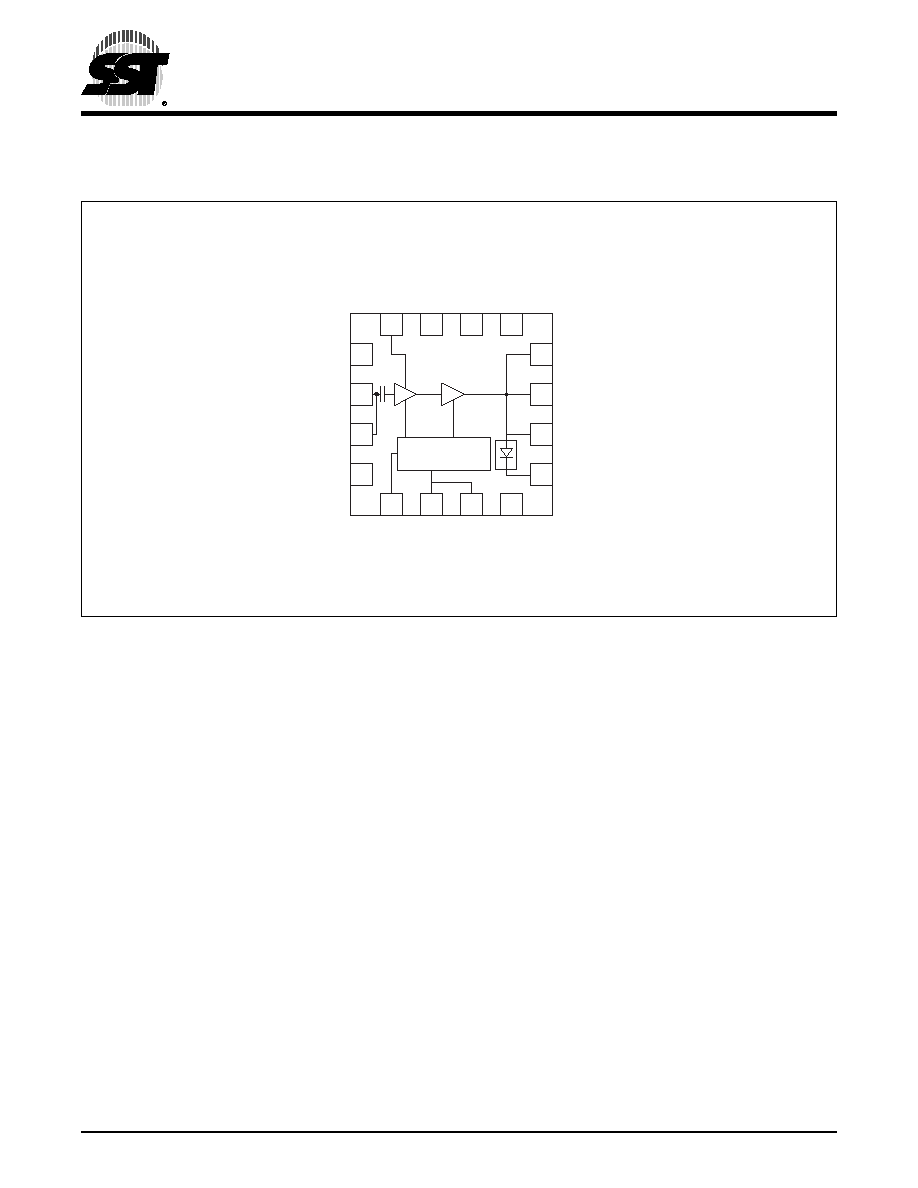
FUNCTIONAL BLOCKS
2
5
6
8
16
VCC
1
15
1
14
NC
NC
4
9
11
12
10
13
NC
VCC
b
VRE
F
VRE
F
NC
VCC2
RFOUT
RFOUT
Det
NC
3
RFIN
RFIN
NC
Bias Circuit
7
1300 B1.0
F
UNCTIONAL
B
LOCK
D
IAGRAM
Preliminary Specifications
2.4 GHz High-Power, High-Gain Power Amplifier
SST12LP14A
3
©2005 SST Communications Corp.
S71300-01-000
9/05
PIN ASSIGNMENTS
FIGURE 1: P
IN
A
SSIGNMENTS
FOR
16-
CONTACT
VQFN
PIN DESCRIPTIONS
TABLE 1: P
IN
D
ESCRIPTION
Symbol
Pin No.
Pin Name
Type
1
1. I=Input, O=Output
Function
GND
0
Ground
The center pad should be connected to RF ground with
several low inductance, low resistance vias
NC
1
No Connection
Unconnected pin
RFIN
2
I
RF input, DC decoupled
RFIN
3
I
RF input, DC decoupled
NC
4
No Connection
Unconnected pin
VCCb
5
Power Supply
PWR
Supply voltage for bias circuit
VREF
6
PWR
1
st
and 2
nd
stage idle current control
VREF
7
PWR
1
st
and 2
nd
stage idle current control
NC
8
No Connection
Unconnected pin
Det
9
O
On-chip power detector
RFOUT
10
O
RF output
RFOUT
11
O
RF output
VCC2
12
Power Supply
PWR
Power supply, 2
nd
stage
NC
13
No Connection
Unconnected pin
NC
14
No Connection
Unconnected pin
NC
15
No Connection
Unconnected pin
VCC1
16
Power Supply
PWR
Power supply, 1
st
stage
T1.0 1300
5
6
8
16
V
C
C
1
15
14
N
C
N
C
9
11
12
10
13
N
C
V
C
C
b
V
R
E
F
V
R
E
F
N
C
VCC2
RFOUT
RFOUT
Det
2
1
4
3
NC
RFIN
RFIN
NC
7
1300 16-vqfn P1.0
Top View
(contacts facing down)
RF and DC GND
0
Preliminary Specifications
2.4 GHz High-Power, High-Gain Power Amplifier
SST12LP14A
©2005 SST Communications Corp.
S71300-01-000
9/05
4
ELECTRICAL SPECIFICATIONS
The AC and DC specifications for the power amplifier interface signals. Refer to Table 2 for the DC voltage and current spec-
ifications. Refer to Figures 2 through 18 for the RF performance.
Absolute Maximum Stress Ratings (Applied conditions greater than those listed under "Absolute Maximum
Stress Ratings" may cause permanent damage to the device. This is a stress rating only and functional operation
of the device at these conditions or conditions greater than those defined in the operational sections of this data
sheet is not implied. Exposure to absolute maximum stress rating conditions may affect device reliability.)
Input power to pins 2 and 3 (P
IN
) . . . . . . . . . . . . . . . . . . . . . . . . . . . . . . . . . . . . . . . . . . . . . . . . . . . . . . . . . . +5 dBm
Average output power (P
OUT
). . . . . . . . . . . . . . . . . . . . . . . . . . . . . . . . . . . . . . . . . . . . . . . . . . . . . . . . . . . . +26 dBm
Supply Voltage at pins 5, 12, and 16 (V
CC
) . . . . . . . . . . . . . . . . . . . . . . . . . . . . . . . . . . . . . . . . . . . . . -0.3V to +4.6V
Reference voltage to pins 6 and 7 (V
REF
) . . . . . . . . . . . . . . . . . . . . . . . . . . . . . . . . . . . . . . . . . . . . . . -0.3V to +3.6V
DC supply current (I
CC
) . . . . . . . . . . . . . . . . . . . . . . . . . . . . . . . . . . . . . . . . . . . . . . . . . . . . . . . . . . . . . . . . . 400 mA
Operating Temperature (T
A
) . . . . . . . . . . . . . . . . . . . . . . . . . . . . . . . . . . . . . . . . . . . . . . . . . . . . . . . . -40∫C to +85∫C
Storage Temperature (T
STG
) . . . . . . . . . . . . . . . . . . . . . . . . . . . . . . . . . . . . . . . . . . . . . . . . . . . . . . -40∫C to +120∫C
Maximum Junction Temperature (T
J
) . . . . . . . . . . . . . . . . . . . . . . . . . . . . . . . . . . . . . . . . . . . . . . . . . . . . . . . +150∫C
Surface Mount Solder Reflow Temperature
1
. . . . . . . . . . . . . . . . . . . . . . . . . . . . . . . . . . . . . . 260∞C for 10 seconds
1. Please consult the factory for the latest information.
O
PERATING
R
ANGE
Range
Ambient Temp
V
CC
Industrial
-40∞C to +85∞C
3.3V
TABLE
2: DC E
LECTRICAL
C
HARACTERISTICS
Symbol
Parameter
Min.
Typ
Max.
Unit
Test Conditions
V
CC
Supply Voltage at pins 5, 12, 16
3.0
3.3
4.2
V
I
CC
Supply Current
for 802.11g, 22 dBm
210
mA
for 802.11b, 23 dBm
230
mA
I
CQ
Idle current for 802.11g to meet EVM<4% @ 21.5dBm
70
mA
I
OFF
Shut down current
0.1
µA
V
REG
Reference Voltage for, with 110
resistor
2.75
2.85
2.95
V
T2.0 1300
Preliminary Specifications
2.4 GHz High-Power, High-Gain Power Amplifier
SST12LP14A
5
©2005 SST Communications Corp.
S71300-01-000
9/05
TABLE
3: AC E
LECTRICAL
C
HARACTERISTICS
FOR
C
ONFIGURATION
Symbol
Parameter
Min.
Typ
Max.
Unit
F
L-U
Frequency range
2400
2485
MHz
P
OUT
Output power
@ PIN = -6 dBm 11b signals
22
dBm
@ PIN = -7 dBm 11g signals
21
dBm
G
Small signal gain
28
29
dB
G
VAR1
Gain variation over band (2400~2485 MHz)
±0.5
dB
G
VAR2
Gain ripple over channel (20 MHz)
0.2
dB
ACPR
Meet 11b spectrum mask
22
23
dBm
Meet 11g OFDM 54 Mbps spectrum mask
22
23
dBm
Added EVM
@ 21.5 dBm output with 11g OFDM 54 Mbps signal
4
%
2f, 3f, 4f, 5f
Harmonics at 22 dBm, without external filters
-40
dBc
T3.1 1300
Preliminary Specifications
2.4 GHz High-Power, High-Gain Power Amplifier
SST12LP14A
©2005 SST Communications Corp.
S71300-01-000
9/05
6
TYPICAL PERFORMANCE CHARACTERISTICS
T
EST
C
ONDITIONS
: V
CC
= 3.3V, T
A
= 25∞C,
UNLESS
OTHERWISE
SPECIFIED
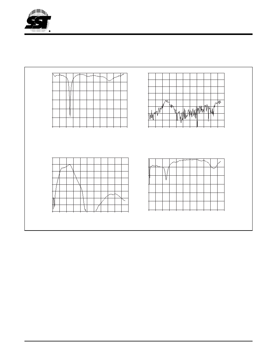
FIGURE 2: S-P
ARAMETERS
-80
-70
-60
-50
-40
-30
-20
-10
0
0.0
1.0
2.0
3.0
4.0
5.0
6.0
7.0
8.0
9.0
10.0
11.0
-30
-25
-20
-15
-10
-5
0
0.0
1.0
2.0
3.0
4.0
5.0
6.0
7.0
8.0
9.0
10.0 11.0
-40
-30
-20
-10
0
10
20
30
40
0.0
1.0
2.0
3.0
4.0
5.0
6.0
7.0
8.0
9.0
10.0
11.0
-30
-25
-20
-15
-10
-5
0
0.0
1.0
2.0
3.0
4.0
5.0
6.0
7.0
8.0
9.0
10.0 11.0
Frequency (GHz)
S11 (dB)
Frequency (GHz)
S21 (dB)
S22 (dB)
Frequency (GHz)
S12 (dB)
Frequency (GHz)
1300 S-Parms.0.0
Preliminary Specifications
2.4 GHz High-Power, High-Gain Power Amplifier
SST12LP14A
7
©2005 SST Communications Corp.
S71300-01-000
9/05
TWO-TONE MEASUREMENTS
T
EST
C
ONDITIONS
:
F
= 1 MH
Z
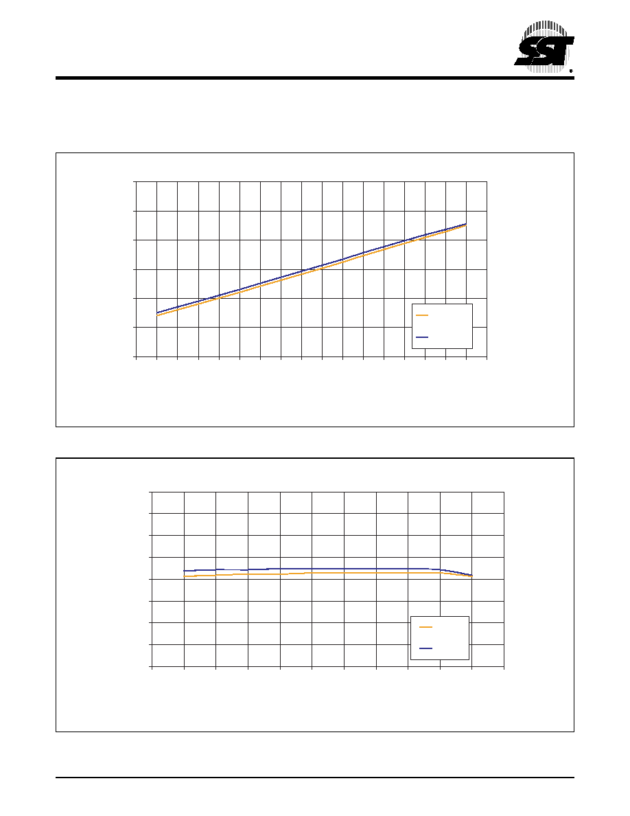
FIGURE 3: O
UTPUT
P
OWER
VERSUS
I
NPUT
P
OWER
FIGURE 4: P
OWER
G
AIN
VERSUS
O
UTPUT
P
OWER
0
5
10
15
20
25
30
-21
-20
-19
-18
-17
-16
-15
-14
-13
-12
-11
-10
-9
-8
-7
-6
-5
-4
2.412 GHz
2.472 GHz
1300 PoutVPin.0.0
Input Power (dBm)
Output Power (dBm)
20
22
24
26
28
30
32
34
36
14
15
16
17
18
19
20
21
22
23
24
25
Output Power (dBm)
Power Gain (dB)
2.412 GHz
2.472 GHz
1300 GainVsP
out.0.0
Preliminary Specifications
2.4 GHz High-Power, High-Gain Power Amplifier
SST12LP14A
©2005 SST Communications Corp.
S71300-01-000
9/05
8
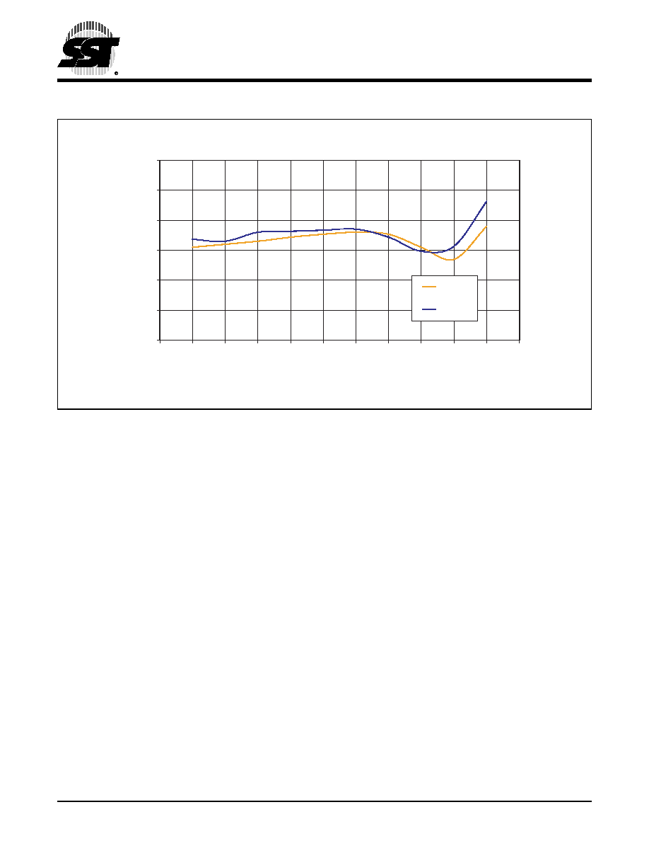
FIGURE 5: IMD3
VERSUS
O
UTPUT
P
OWER
-50
-45
-40
-35
-30
-25
-20
14
15
16
17
18
19
20
21
22
23
24
25
IMD3 (dBc)
2.412 GHz
2.472 GHz
Output Power (dBm)
1300 IMD3vsPout.0.0
Preliminary Specifications
2.4 GHz High-Power, High-Gain Power Amplifier
SST12LP14A
9
©2005 SST Communications Corp.
S71300-01-000
9/05
TYPICAL PERFORMANCE CHARACTERISTICS
T
EST
C
ONDITIONS
: V
CC
= 3.3V, T
A
= 25∞C, 54 M
BPS
802.11
G
OFDM
SIGNAL
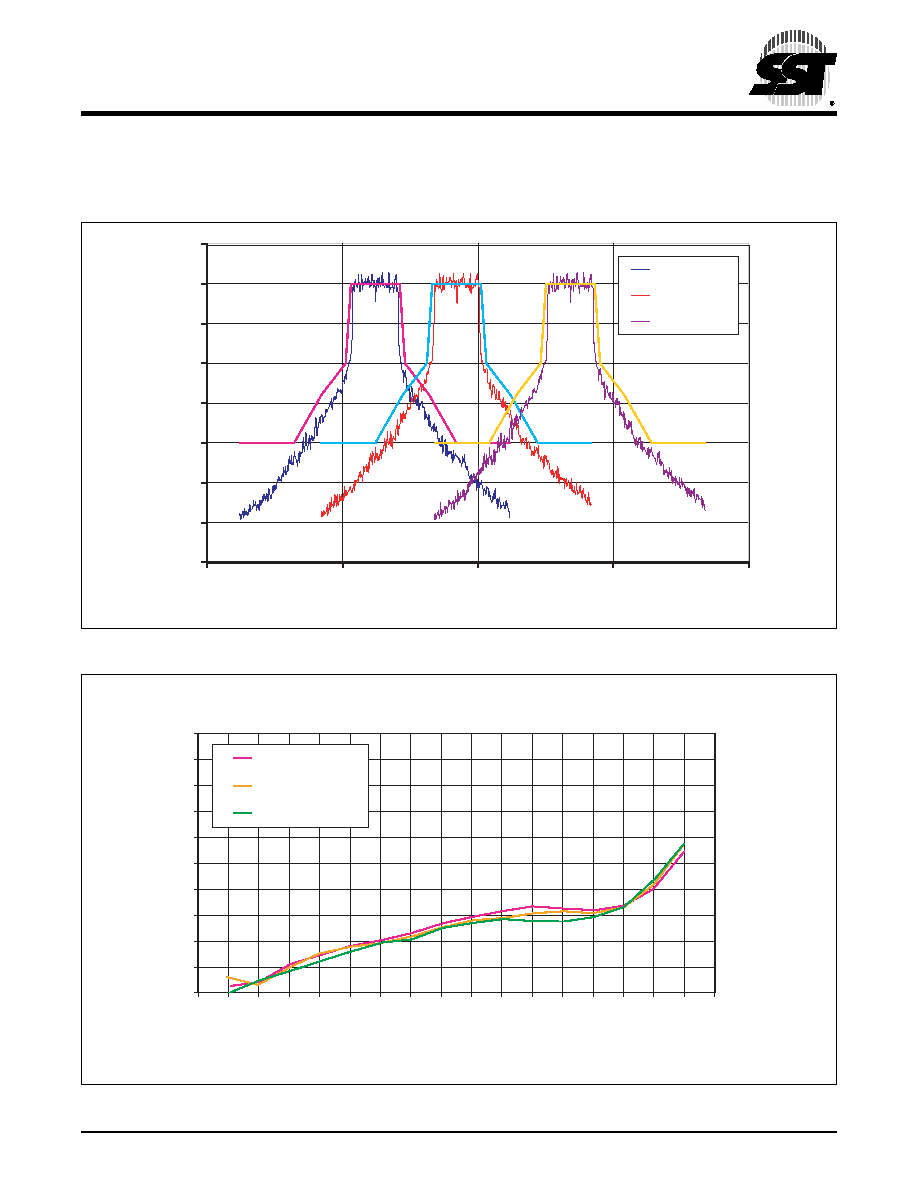
FIGURE 6: 802.11
G
S
PECTRUM
M
ASK
AT
23
D
B
M
FIGURE 7: EVM
VS
O
UTPUT
P
OWER
-70
-60
-50
-40
-30
-20
-10
0
10
2.3 5
2.4 0
2.45
2.50
2.55
Freq = 2.412 GHZ
Freq = 2.442 GHz
Freq = 2.484 GHz
Frequency (GHz)
1300 AmpVSFreq.0.0
Amplitude (dB)
0
1
2
3
4
5
6
7
8
9
10
7
8
9
10
11
12
13
14
15
16
17
18
19
20
21
22
23
24
Output Power (dBm)
EVM (%)
Freq = 2.412 GHz
Freq = 2.442 GHz
Freq = 2.484 GHz
1300 EVMvsPout.0.0
Preliminary Specifications
2.4 GHz High-Power, High-Gain Power Amplifier
SST12LP14A
©2005 SST Communications Corp.
S71300-01-000
9/05
10
FIGURE 8: T
OTAL
C
URRENT
C
ONSUMPTION
FOR
802.11
G
O
PERATION
75
10 0
12 5
15 0
17 5
20 0
22 5
25 0
27 5
9
10
11
12
13
14
15
16
17
18
19
20
21
22
23
24
2.412 GHz
2.442 GHz
2.484 GHz
Output Power (dBm)
Supply Current (mA)
1300 CurrVPout.0.0
Preliminary Specifications
2.4 GHz High-Power, High-Gain Power Amplifier
SST12LP14A
11
©2005 SST Communications Corp.
S71300-01-000
9/05
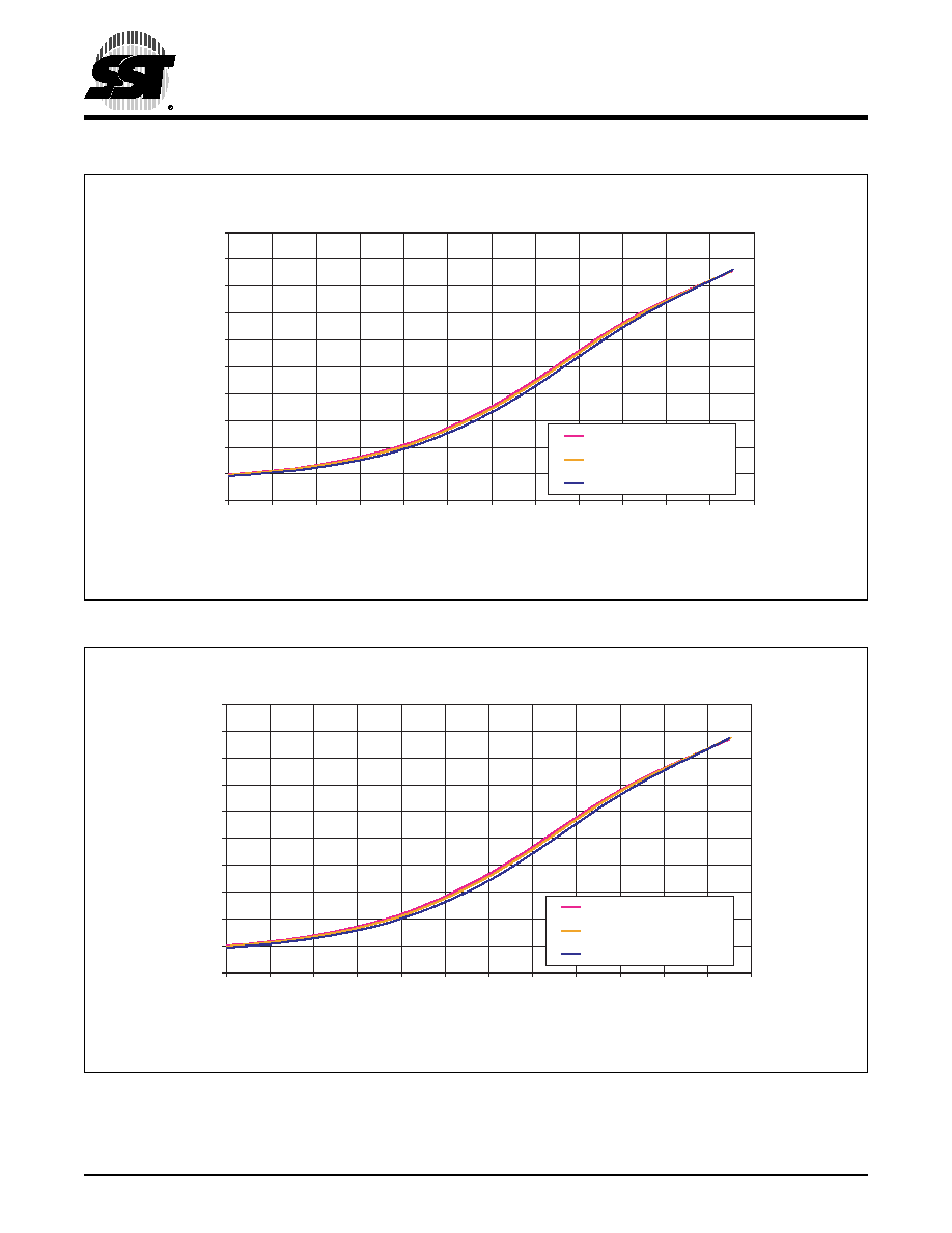
FIGURE 9: CH1 D
ETECTOR
C
HARACTERISTICS
O
VER
T
EMPERATURE
WITH
2:1 O
UTPUT
VSWR A
LL
P
HASES
FIGURE 10: CH7 D
ETECTOR
C
HARACTERISTICS
O
VER
T
EMPERATURE
WITH
2:1 O
UTPUT
VSWR A
LL
P
HASES
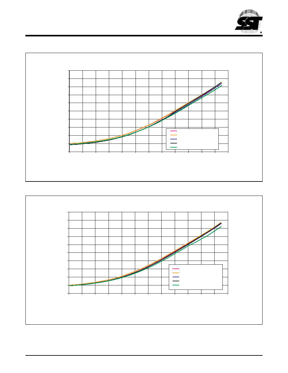
0.60
0.70
0.80
0.90
1.00
1.10
1.20
1.30
1.40
1.50
1.60
0
2
4
6
8
10
12
14
16
18
20
22
24
Freq = 2.412 GHz (0 C)
Output Power (dBm)
Detector V
olta
g
e
(V)
1300 CH1_OFDM.0.0
Freq = 2.412 GHz (25 C)
Freq = 2.412 GHz (85 C)
Freq = 2.412 GHz (Min)
Freq = 2.412 GHz (Max)
0.60
0.70
0.80
0.90
1.00
1.10
1.20
1.30
1.40
1.50
1.60
0
2
4
6
8
10
12
14
16
18
20
22
24
Output Power (dBm)
Detector V
olta
g
e
(V)
1300 CH7_OFDM.0.0
Freq = 2.442 GHz (0 C)
Freq = 2.442 GHz (25 C)
Freq = 2.442 GHz (85 C)
Freq = 2.442 GHz (Min)
Freq = 2.442 GHz (Max)
Preliminary Specifications
2.4 GHz High-Power, High-Gain Power Amplifier
SST12LP14A
©2005 SST Communications Corp.
S71300-01-000
9/05
12
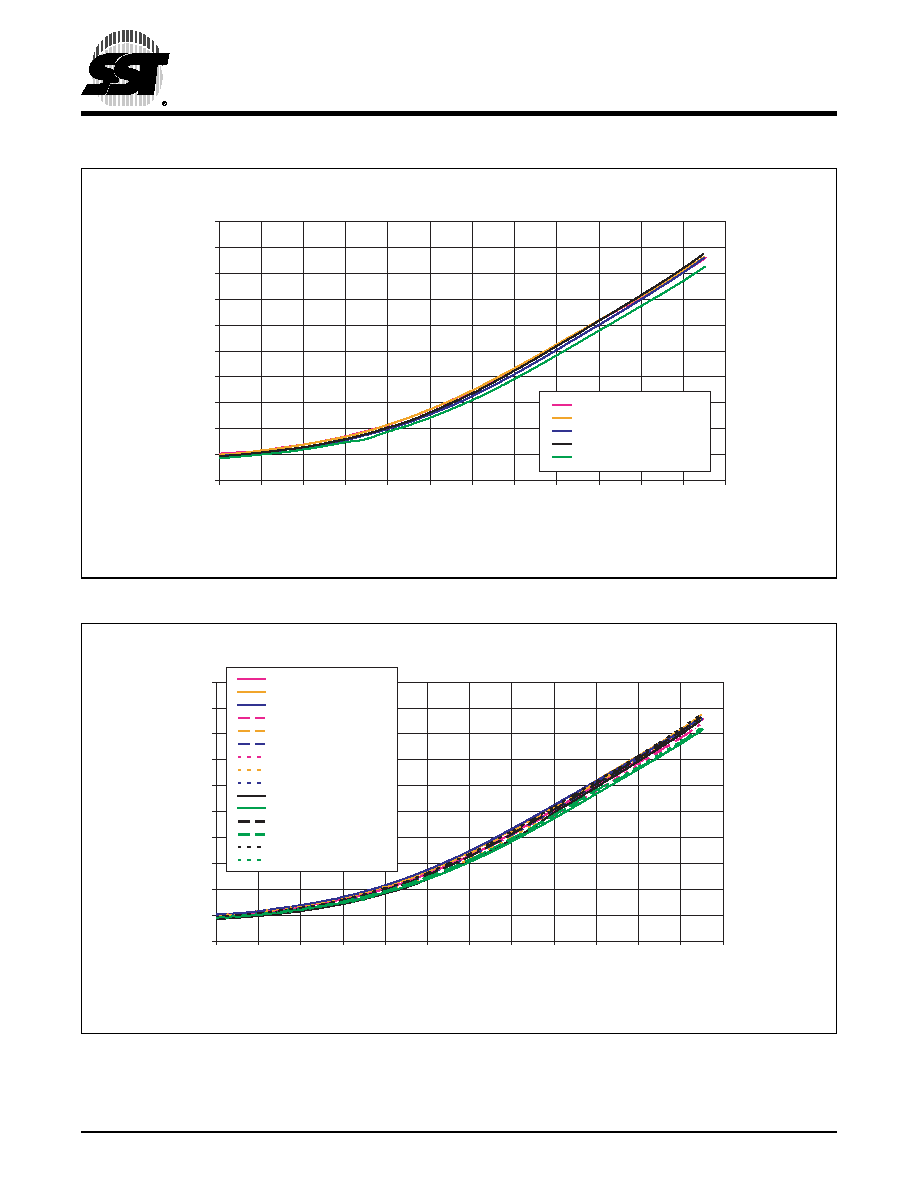
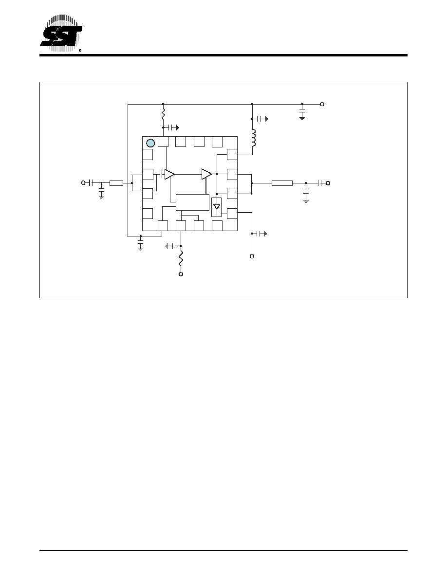
FIGURE 11: CH14 D
ETECTOR
C
HARACTERISTICS
O
VER
T
EMPERATURE
WITH
2:1 O
UTPUT
VSWR A
LL
P
HASES
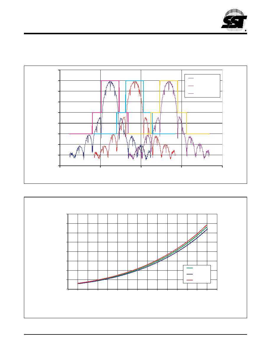
FIGURE 12: D
ETECTOR
C
HARACTERISTICS
O
VER
T
EMPERATURE
AND
O
VER
F
REQUENCY
WITH
2:1 O
UTPUT
VSWR
A
LL
P
HASES
0.60
0.70
0.80
0.90
1.00
1.10
1.20
1.30
1.40
1.50
1.60
0
2
4
6
8
10
12
14
16
18
20
22
24
Output Power (dBm)
Detector V
olta
g
e
(V)
Freq = 2.484 GHz (0 C)
Freq = 2.484 GHz (25 C)
Freq = 2.484 GHz (85 C)
Freq = 2.484 GHz (Min)
Freq = 2.484 GHz (Max)
1300 CH14_OFDM.0.0
0.60
0.70
0.80
0.90
1.00
1.10
1.20
1.30
1.40
1.50
1.60
0
2
4
6
8
10
12
14
16
18
20
22
24
Output Power (dBm)
Detector V
olta
g
e
(V)
1300 CHA_OFDM.0.0
Freq = 2.442 GHz (0 C)
Freq = 2.412 GHz (25 C)
Freq = 2.484 GHz (85 C)
Freq = 2.412 GHz (Min)
Freq = 2.412 GHz (Max)
Freq = 2.442 GHz (Min)
Freq = 2.442 GHz (Max)
Freq = 2.484 GHz (Min)
Freq = 2.484 GHz (Max)
Freq = 2.442 GHz (85 C)
Freq = 2.412 GHz (85 C)
Freq = 2.484 GHz (25 C)
Freq = 2.442 GHz (25 C)
Freq = 2.412 GHz (0 C)
Freq = 2.484 GHz (0 C)
Preliminary Specifications
2.4 GHz High-Power, High-Gain Power Amplifier
SST12LP14A
13
©2005 SST Communications Corp.
S71300-01-000
9/05
TYPICAL PERFORMANCE CHARACTERISTICS
T
EST
C
ONDITIONS
: V
CC
= 3.3V, T
A
= 25∞C, 1 M
BPS
802.11B CCK
SIGNAL
FIGURE 13: 802.11B S
PECTRUM
M
ASK
AT
23
D
B
M
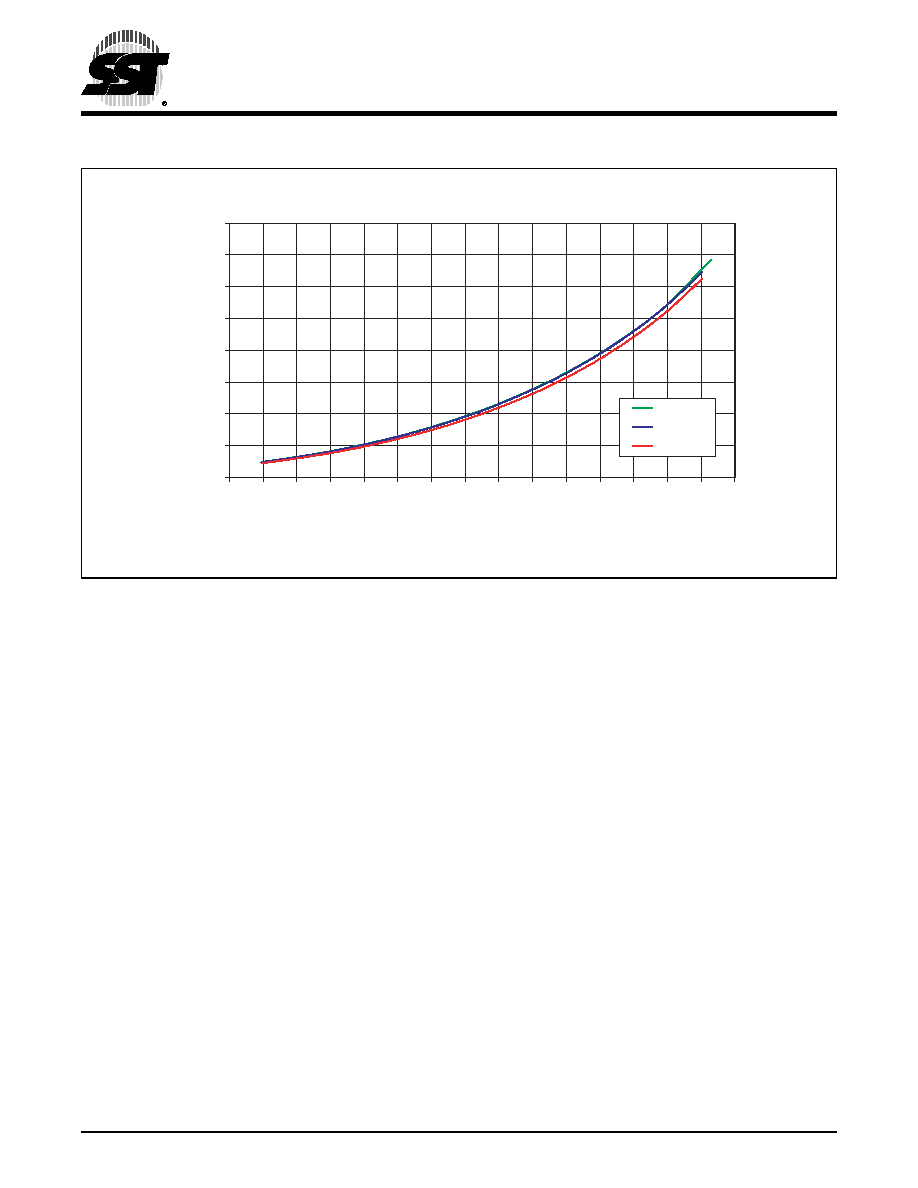
FIGURE 14: T
OTAL
C
URRENT
C
ONSUMPTION
FOR
802.11B O
PERATION
-80
-70
-60
-50
-40
-30
-20
-10
0
10
2.35
2. 40
2.45
2. 50
2.55
Freq = 2.412 GHZ
Freq = 2.442 GHz
Freq = 2.484 GHz
Frequency (GHz)
1300 AmpVSFreqCCK.0.0
Amplitude (dB)
75
100
125
150
175
200
225
250
275
9
10
11
12
13
14
15
16
17
18
19
20
21
22
23
24
Output Power (dBm)
Supply Current (mA)
1300 CurrVPoutCCK.0.0
2.412 GHz
2.442 GHz
2.484 GHz
Preliminary Specifications
2.4 GHz High-Power, High-Gain Power Amplifier
SST12LP14A
©2005 SST Communications Corp.
S71300-01-000
9/05
14
FIGURE 15: CH1 D
ETECTOR
C
HARACTERISTICS
O
VER
T
EMPERATURE
FIGURE 16: CH7 D
ETECTOR
C
HARACTERISTICS
O
VER
T
EMPERATURE
0.60
0.70
0.80
0.90
1.00
1.10
1.20
1.30
1.40
1.50
1.60
0
2
4
6
8
10
12
14
16
18
20
22
24
Output Power (dBm)
Detector V
olta
g
e
(V)
1300 CH1_OFDM.0.0
Freq = 2.412 GHz (0 C)
Freq = 2.412 GHz (25 C)
Freq = 2.412 GHz (85 C)
0.60
0.70
0.80
0.90
1.00
1.10
1.20
1.30
1.40
1.50
1.60
0
2
4
6
8
10
12
14
16
18
20
22
24
Output Power (dBm)
Detector V
olta
g
e
(V)
1300 CH7_CCK.0.0
Freq = 2.442 GHz (0 C)
Freq = 2.442 GHz (25 C)
Freq = 2.442 GHz (85 C)

Preliminary Specifications
2.4 GHz High-Power, High-Gain Power Amplifier
SST12LP14A
15
©2005 SST Communications Corp.
S71300-01-000
9/05
TYPICAL PERFORMANCE CHARACTERISTICS
T
EST
C
ONDITIONS
: V
CC
= 3.3V, T
A
=25∞C, 1 M
BPS
802.11B CCK
SIGNAL
FIGURE 17: CH14 D
ETECTOR
C
HARACTERISTICS
O
VER
T
EMPERATURE
FIGURE 18: D
ETECTOR
C
HARACTERISTICS
O
VER
T
EMPERATURE
AND
F
REQUENCY
0.60
0.70
0.80
0.90
1.00
1.10
1.20
1.30
1.40
1.50
1.60
0
2
4
6
8
10
12
14
16
18
20
22
24
Freq = 2.484 GHz (0 C)
Freq = 2.484 GHz (25 C)
Freq = 2.484 GHz (85 C)
1300 CH14_CCK.0.0
Output Power (dBm)
Detector V
olta
g
e
(V)
0.60
0.70
0.80
0.90
1.00
1.10
1.20
1.30
1.40
1.50
1.60
0
2
4
6
8
10
12
14
16
18
20
22
24
Output Power (dBm)
Detector V
olta
g
e
(V)
1300 CHA_CCK.0.0
Freq = 2.442 GHz (0 C)
Freq = 2.412 GHz (25 C)
Freq = 2.484 GHz (85 C)
Freq = 2.442 GHz (85 C)
Freq = 2.412 GHz (85 C)
Freq = 2.484 GHz (25 C)
Freq = 2.442 GHz (25 C)
Freq = 2.412 GHz (0 C)
Freq = 2.484 GHz (0 C)
Preliminary Specifications
2.4 GHz High-Power, High-Gain Power Amplifier
SST12LP14A
©2005 SST Communications Corp.
S71300-01-000
9/05
16
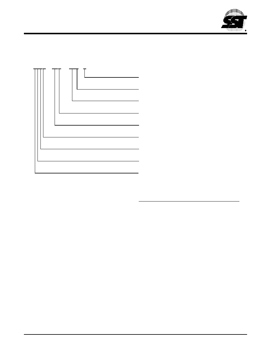
FIGURE 19: T
YPICAL
S
CHEMATIC
FOR
H
IGH
-P
OWER
/H
IGH
-E
FFICIENCY
802.11
B
/
G
A
PPLICATIONS
2
5
6
7
8
9
11
16
15
Bias circuit
1
50
/225 mil
50
RFOUT
100 pF
47 pF
2.4 pF
50
/ 120 mil
50
RFin
VREG
14
13
22 µF
0.1 µF
Vcc
4
12
10
27 nH / 0805
R1 110
3
0.1 µF
Det
10 pF
1300 Schematic.0.1
Suggested operation conditions:
1. V
CC
= 3.3V
2. Center slug to RF ground
3. VREG=2.85V with R1=110
4. R2=0-40
depending on ruggedness
requirement under overdrive
* Can be replaced by a ~1.2 nH
chip inductor for compactness
47 pF
2.0 pF
0.1 µF
R2
Preliminary Specifications
2.4 GHz High-Power, High-Gain Power Amplifier
SST12LP14A
17
©2005 SST Communications Corp.
S71300-01-000
9/05
PRODUCT ORDERING INFORMATION
Valid combinations for SST12LP14A
SST12LP14A-QVC
SST12LP14A-QVCE
SST12LP14A Evaluation Kits
SST12LP14A-QVC-K
SST12LP14A-QVCE-K
Note: Valid combinations are those products in mass production or will be in mass production. Consult your SST sales
representative to confirm availability of valid combinations and to determine availability of new combinations.
SST12LP
14A - QVC
E
SSTXXLP
XXX -
XXX
X
Environmental Attribute
E
1
= non-Pb contact (lead) finish
Package Modifier
C = 16 contact
Package Type
QV = VQFN
Version
Product Family Identifier
Product Type
P = Power Amplifier
Voltage
L = 3.0-3.6V
Frequency of Operation
2 = 2.4 GHz
Product Line
1 = SST Communications
1. Environmental suffix "E" denotes non-Pb solder.
SST non-Pb solder devices are "RoHS Compliant".
Preliminary Specifications
2.4 GHz High-Power, High-Gain Power Amplifier
SST12LP14A
©2005 SST Communications Corp.
S71300-01-000
9/05
18
PACKAGING DIAGRAMS
16-
CONTACT
V
ERY
-
THIN
Q
UAD
F
LAT
N
O
-
LEAD
(VQFN)
SST P
ACKAGE
C
ODE
: QVC
TABLE
4: R
EVISION
H
ISTORY
Revision
Description
Date
00
∑
Initial release of data sheet
Jun 2005
01
∑
Removed Stability and Ruggedness parms from Table 3 on page 5
∑
Updated the schematic in Figure 19 on page 16
Sep 2005
Note: 1. Complies with JEDEC JEP95 MO-220I, variant VEED except external paddle nominal dimensions.
2. From the bottom view, the pin #1 indicator may be either a 45-degree chamfer or a half-circle notch.
3. The external paddle is electrically connected to the die back-side and possibly to certain V
SS
leads.
This paddle can be soldered to the PC board; it is suggested to connect this paddle to the V
SS
of the unit.
Connection of this paddle to any other voltage potential can result in shorts and/or electrical malfunction of the device.
4. Untoleranced dimensions are nominal target dimensions.
5. All linear dimensions are in millimeters (max/min).
16-vqfn-3x3-QVC-0.0
1.7
0.5 BSC
See notes
2 and 3
Pin #1
0.30
0.18
0.076
1.7
0.2
3.00 ± 0.10
3.00 ± 0.10
0.05 Max
0.45
0.35
1.00
0.80
Pin #1
TOP VIEW
BOTTOM VIEW
SIDE VIEW
1mm

Preliminary Specifications
2.4 GHz High-Power, High-Gain Power Amplifier
SST12LP14A
19
©2005 SST Communications Corp.
S71300-01-000
9/05
CONTACT INFORMATION
Marketing
SST Communications Corp.
5340 Alla Road, Ste. 210
Los Angeles, CA 90066
Tel: 310-577-3600
Fax: 310-577-3605
Sales
NORTH AMERICA
ASIA PACIFIC NORTH
Silicon Storage Technology, Inc.
SST Macao
Les Crowder
H. H. Chang
Technical Sales Support - North America
Senior Director, Sales
Tel: 949-495-6437
Room N, 6th Floor,
Fax: 949-495-6364
Macao Finance Center, No. 202A-246,
E-mail: lcrowder@sst.com
Rua de Pequim, Macau
Tel: (853) 706-022
Fax: (853) 706-023
E-mail: hchang@sst.com
EUROPE
ASIA PACIFIC SOUTH
Silicon Storage Technology Ltd.
SST Communications Co.
Ralph Thomson
Sunny Tzeng
Applications Manager
Sales Manager
Mark House
4F-2, No. 24, Lane 123, Sec.6,
9-11 Queens Road
Min Chuan E. Rd
Hersham KT12 5LU
UK
Taipei 114, Taiwan, R.O.C.
Tel: +44 (0) 1869 321 431
Tel: +886-22795-6877 Ext. 163
Cell: +44 (0) 7787 508 919
Fax: +886-9792-1241
E-mail: rthomson@sst.com
E-mail: stzeng@sst.com
JAPAN
KOREA
SST Japan
SST Korea
Jun Kamata
Charlie Shin
Sales Director
Country Manager
9F Toshin-Tameike Bldg, 1-1-14 Akasaka,
Rm# 1101 DonGu Root Bldg, 16-2 Sunae-Dong,
Minato-ku, Tokyo, Japan 107-0052
Bundang-Gu, Sungnam, Kyunggi-Do
Tel: (81) 3-5575-5515
Korea, 463-020
Fax: (81) 3-5575-5516
Tel: (82) 31-715-9138
Email: jkamata@sst.com
Fax: (82) 31-715-9137
Email: cshin@sst.com
Silicon Storage Technology, Inc. ∑ 1171 Sonora Court ∑ Sunnyvale, CA 94086 ∑ Telephone 408-735-9110 ∑ Fax 408-735-9036
www.SuperFlash.com or www.sst.com