
©2006 SST Communications Corp.
S71291-02-000
7/06
1
The SST logo and SuperFlash are registered Trademarks of Silicon Storage Technology, Inc.
These specifications are subject to change without notice.
Data Sheet
FEATURES:
∑
High Gain:
≠ Typically 32 dB gain across 2.4≠2.5 GHz over
temperature 0∞C to +85∞C
∑
High linear output power:
≠ >29 dBm P1dB
- Please refer to "Absolute Maximum Stress
Ratings" on page 4
≠ Meets 802.11g OFDM ACPR requirement up to
25 dBm
≠ Added EVM~4% up to 23 dBm for
54 Mbps 802.11g signal
≠ Added EVM~3.5% up to 23 dBm for
application over 2.3≠2.4 GHz or
2.5≠2.6 GHz WiBro/WiMax frequency bands
≠ Meets 802.11b ACPR requirement up to 25 dBm
∑
High power-added efficiency/Low operating
current for both 802.11g/b applications
≠ ~26%/300 mA @ P
OUT
= 24 dBm for 802.11g
≠ ~27%/350 mA @ P
OUT
= 25 dBm for 802.11b
∑
Built-in Ultra-low I
REF
power-up/down control
≠ I
REF
~2 mA
∑
Low idle current
≠ ~70 mA I
CQ
∑
High-speed power-up/down
≠ Turn on/off time (10%-90%) <100 ns
≠ Typical power-up/down delay with driver delay
included <200 ns
∑
High temperature stability
≠ ~1 dB gain/power variation between 0∞C to +85∞C
≠ ~1 dB detector variation over 0∞C to +85∞C
∑
Low shut-down current (< 0.1 µA)
∑
On-chip power detection
∑
25 dB dynamic range on-chip power detection
∑
Simple input/output matching
∑
Packages available
≠ 16-contact VQFN (3mm x 3mm)
∑
All non-Pb (lead-free) devices are RoHS compliant
APPLICATIONS:
∑
WLAN (IEEE 802.11g/b)
∑
Home RF
∑
Cordless phones
∑
2.4 GHz ISM wireless equipment
PRODUCT DESCRIPTION
The SST12LP15A is a high-power and high-gain power
amplifier based on the highly-reliable InGaP/GaAs HBT
technology.
The SST12LP15A can be easily configured for high-power
applications with superb power-added efficiency while
operating over the 2.4-2.5 GHz frequency band. It typically
provides 32 dB gain with 26% power-added efficiency @
P
OUT
= 24 dBm for 802.11g and 27% power-added effi-
ciency @ P
OUT
= 25 dBm for 802.11b.
The SST12LP15A has excellent linearity, typically ~4%
added EVM at 23 dBm output power which is essential for
54 Mbps 802.11g operation while meeting 802.11g spec-
trum mask at 25 dBm. This device can be configured for
applications with an added EVM of approximately 3.5%, up
to 23 dBm over 2.3≠2.4 GHz or 2.5≠2.6 GHz WiBro/
WiMax frequency bands. SST12LP15A also has wide-
range (>25 dB), temperature-stable (~1 dB over 85∞C), sin-
gle-ended/differential power detectors which lower users'
cost on power control.
The power amplifier IC also features easy board-level
usage along with high-speed power-up/down control. Ultra-
low reference current (total I
REF
~2 mA) makes the
SST12LP15A controllable by an on/off switching signal
directly from the baseband chip. These features coupled
with low operating current make the SST12LP15A ideal for
the final stage power amplification in battery-powered
802.11g/b WLAN transmitter applications.
The SST12LP15A is offered in 16-contact VQFN package.
See Figure 2 for pin assignments and Table 1 for pin
descriptions.
2.4 GHz High-Power and High-Gain Power Amplifier
SST12LP15A
SST-GP1215A2.4 GHz High Gain High Power PA

Data Sheet
2.4 GHz High-Power and High-Gain Power Amplifier
SST12LP15A
©2006 SST Communications Corp.
S71291-02-000
7/06
2
FUNCTIONAL BLOCKS
FIGURE 1: Functional Block Diagram
2
5
6
8
16
VCC1
15
1
14
VCC2
NC
4
9
11
12
10
13
NC
VCCb
VREF1
VREF2
Det_ref
VCC3
RFOUT
RFOUT
Det
NC
3
RFIN
RFIN
NC
Bias Circuit
7
1291 B1.0

Data Sheet
2.4 GHz High-Power and High-Gain Power Amplifier
SST12LP15A
3
©2006 SST Communications Corp.
S71291-02-000
7/06
PIN ASSIGNMENTS
FIGURE 2: Pin Assignments for 16-contact VQFN
PIN DESCRIPTIONS
TABLE
1: Pin Description
Symbol
Pin No.
Pin Name
Type
1
1. I=Input, O=Output
Function
GND
0
Ground
The center pad should be connected to RF ground with
several low inductance, low resistance vias.
NC
1
No Connection
Unconnected pins.
RFIN
2
I
RF input, DC decoupled
RFIN
3
I
RF input, DC decoupled
NC
4
No Connection
Unconnected pins.
VCCb
5
Power Supply
PWR
Supply voltage for bias circuit
VREF1
6
PWR
1st and 2nd stage idle current control
VREF2
7
PWR
3rd stage idle current control
Det_ref
8
O
On-chip power detector reference
Det
9
O
On-chip power detector
RFOUT
10
O
RF output
RFOUT
11
O
RF output
VCC3
12
Power Supply
PWR
Power supply, 3rd stage
NC
13
No Connection
Unconnected pins.
VCC2
14
Power Supply
PWR
Power supply, 2nd stage
NC
15
No Connection
Unconnected pins.
VCC1
16
Power Supply
PWR
Power supply, 1st stage
T1.0 1291
5
6
8
16
VCC1
15
14
VCC2
NC
9
11
12
10
13
NC
VCCb
VREF1
VREF2
Det_ref
VCC3
RFOUT
RFOUT
Det
2
1
4
3
NC
RFIN
RFIN
NC
7
1291 16-vqfn P1.0
Top View
(contacts facing down)
RF and DC GND
0

Data Sheet
2.4 GHz High-Power and High-Gain Power Amplifier
SST12LP15A
©2006 SST Communications Corp.
S71291-02-000
7/06
4
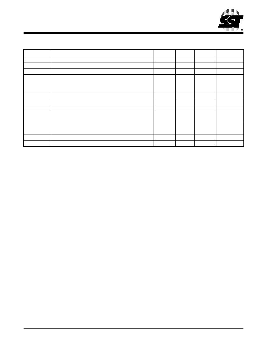
ELECTRICAL SPECIFICATIONS
The AC and DC specifications for the power amplifier interface signals. Refer to Table 2 for the DC voltage and current spec-
ifications. Refer to Figures 3 through 12 for the RF performance.
Absolute Maximum Stress Ratings (Applied conditions greater than those listed under "Absolute Maximum
Stress Ratings" may cause permanent damage to the device. This is a stress rating only and functional operation
of the device at these conditions or conditions greater than those defined in the operational sections of this data
sheet is not implied. Exposure to absolute maximum stress rating conditions may affect device reliability.)
Input power to pins 2 and 3 (P
IN
) . . . . . . . . . . . . . . . . . . . . . . . . . . . . . . . . . . . . . . . . . . . . . . . . . . . . . . . . . . +5 dBm
Average output power (P
OUT
)
1
. . . . . . . . . . . . . . . . . . . . . . . . . . . . . . . . . . . . . . . . . . . . . . . . . . . . . . . . . . . +28 dBm
1. Never measure with CW source. Pulsed single-tone source with <50% duty cycle is recommended. Exceeding the maximum rating
of average output power could cause permanent damage to the device.
Supply Voltage at pins 5, 12, 14, 16 (V
CC
) . . . . . . . . . . . . . . . . . . . . . . . . . . . . . . . . . . . . . . . . . . . . . . -0.3V to +4.6V
Reference voltage to pins 6 (V
REF1
) and pin 7 (V
REF2
) . . . . . . . . . . . . . . . . . . . . . . . . . . . . . . . . . . . . -0.3V to +3.6V
DC supply current (I
CC
) . . . . . . . . . . . . . . . . . . . . . . . . . . . . . . . . . . . . . . . . . . . . . . . . . . . . . . . . . . . . . . . . . 500 mA
Operating Temperature (T
A
) . . . . . . . . . . . . . . . . . . . . . . . . . . . . . . . . . . . . . . . . . . . . . . . . . . . . . . . . -40∫C to +85∫C
Storage Temperature (T
STG
) . . . . . . . . . . . . . . . . . . . . . . . . . . . . . . . . . . . . . . . . . . . . . . . . . . . . . . -40∫C to +120∫C
Maximum Junction Temperature (T
J
) . . . . . . . . . . . . . . . . . . . . . . . . . . . . . . . . . . . . . . . . . . . . . . . . . . . . . . . +150∫C
Surface Mount Solder Reflow Temperature . . . . . . . . . . . . . . . . . . . . . . . . . . . . . . . . . . . . . . . 260∞C for 10 seconds
Operating Range
Range
Ambient Temp
V
CC
Industrial
-40∞C to +85∞C
3.3V
TABLE
2: DC Electrical Characteristics
Symbol
Parameter
Min.
Typ
Max.
Unit
Test Conditions
V
CC
Supply Voltage at pins 5, 12, 14, 16
3.0
3.3
4.2
V
I
CC
Supply Current
for 802.11g, 24 dBm
300
mA
for 802.11b, 25 dBm
350
mA
I
CQ
Idle current for 802.11g to meet EVM<4% @ 23dBm
70
mA
I
OFF
Shut down current
0.1
µA
V
REG1
Reference Voltage for 1st Stage, with 169
resistor
2.85
2.90
2.95
V
V
REG2
Reference Voltage for 2nd Stage, with 140
resistor
2.85
2.90
2.95
V
T2.1 1291
Data Sheet
2.4 GHz High-Power and High-Gain Power Amplifier
SST12LP15A
5
©2006 SST Communications Corp.
S71291-02-000
7/06
TABLE
3: AC Electrical Characteristics for Configuration
Symbol
Parameter
Min.
Typ
Max.
Unit
F
L-U
Frequency range in 802.11b/g applications (see Figure 13)
2400
2485
MHz
F
L-U
Frequency range in 2.3-2.4 GHz applications (see Figure 14)
2300
2400
MHz
F
L-U
Frequency range in 2.5-2.6 GHz applications (see Figure 15)
2500
2600
MHz
P
OUT
Output power
@ PIN = -10 dBm 11b signals
23
dBm
@ PIN = -10 dBm 11g signals
23
dBm
G
Small signal gain
31
32
dB
G
VAR1
Gain variation over each band (2400-2485 MHz)
±0.5
dB
G
VAR2
Gain ripple over channel (Gain variation over 20 MHz)
0.2
dB
Output VSWR
Ruggedness
Survivable time@ 25 dBm (to 50
)
54 Mbps OFDM signal when VSWR=10:1 all phases
10
second
ACPR
Meet 11b spectrum mask
24
25
dBm
Meet 11g OFDM 54 MBPS spectrum mask
24
25
dBm
Added EVM
@ 23 dBm output with 11g OFDM 54 MBPS signal
3.5
%
2f, 3f, 4f, 5f
Harmonics at 22 dBm, without trapping capacitors
-40
dBc
T3.2 1291
Data Sheet
2.4 GHz High-Power and High-Gain Power Amplifier
SST12LP15A
©2006 SST Communications Corp.
S71291-02-000
7/06
6
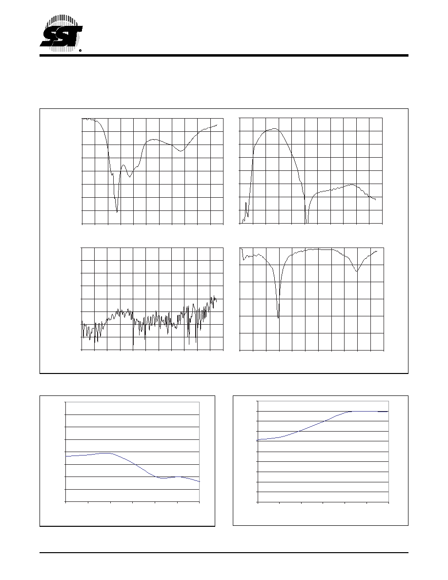
TYPICAL PERFORMANCE CHARACTERISTICS
T
EST
C
ONDITIONS
: V
CC
= 3.3V, T
A
= 25∞C
FIGURE 3: S-Parameters
FIGURE 4: In-band Return Loss
FIGURE 5: In-band Gain Flatness
-40
-35
-30
-25
-20
-15
-10
-5
0
0.0
1.0
2.0
3.0
4.0
5.0
6.0
7.0
8.0
9.0
10.0
11.0
-80
-70
-60
-50
-40
-30
-20
-10
0
0.0
1.0
2.0
3.0
4.0
5.0
6.0
7.0
8.0
9.0
10.0
11.0
-40
-30
-20
-10
0
10
20
30
40
0.0
1.0
2.0
3.0
4.0
5.0
6.0
7.0
8.0
9.0
10.0
11.0
-30
-25
-20
-15
-10
-5
0
0.0
1.0
2.0
3.0
4.0
5.0
6.0
7.0
8.0
9.0
10.0
11.0
S11 (dB)
Frequency (GHz)
S12 (dB)
Frequency (GHz)
S21 (dB)
S22 (dB)
Frequency (GHz)
Frequency (GHz)
1291 S-Parms.0.0
-40.0
-35.0
-30.0
-25.0
-20.0
-15.0
-10.0
-5.0
0.0
2.30
2.35
2.40
2.45
2.50
2.55
2.60
1291 In-band-R.0.0
Return Loss (dB)
Frequency (GHz)
31.0
31.2
31.4
31.6
31.8
32.0
32.2
32.4
32.6
32.8
33.0
2.30
2.35
2.40
2.45
2.50
2.55
2.60
1291 In-band-G.0.0
Gain (dB)
Frequency (GHz)
Data Sheet
2.4 GHz High-Power and High-Gain Power Amplifier
SST12LP15A
7
©2006 SST Communications Corp.
S71291-02-000
7/06
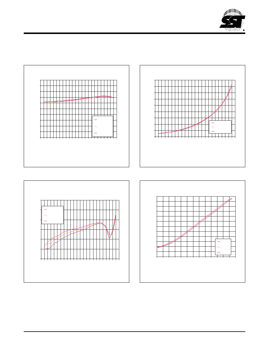
TYPICAL PERFORMANCE CHARACTERISTICS
T
EST
C
ONDITIONS
: F1 = 2.45 GH
Z
, F2 = 2.451 GH
Z
, V
CC
= 3.3V, T
A
= 25∞C
FIGURE 6: Gain vs P
OUT
FIGURE 7: IM3 vs P
OUT
FIGURE 8: I
CC
vs P
OUT
FIGURE 9: Detectors vs P
OUT
20
22
24
26
28
30
32
34
36
38
40
4 5 6 7 8 9 10 11 12 13 14 15 16 17 18 19 20 21 22 23 24 25 26 27 28
Freq=2.412 GHz
Freq=2.442 GHz
F
r
eq=2.484 GHz
Output Power (dBm)
Power Gain (dB)
1291 GainVSPout.0.0
-50
-45
-40
-35
-30
-25
-20
4 5 6 7 8 9 10 11 12 13 14 15 16 17 18 19 20 21 22 23 24 25 26 27 28
Freq=2.
4
12 GHz
Freq=2.442 GHz
Freq=2.484 GHz
Output Power (dBm)
IMD3 (dBc)
1291 IM3VSPout.0.0
50
100
150
200
250
300
350
400
450
500
4 5 6 7 8 9 10 11 12 13 14 15 16 17 18 19 20 21 22 23 24 25 26 27 28
Freq=2.412 GHz
Freq=2.442 GHz
Freq=2.484 GHz
Output Power (dBm)
1291 IccVSPout.0.0
Supply Current (mA)
0.60
0.70
0.80
0.90
1.00
1.10
1.20
1.30
1.40
1.50
1.60
1.70
1.80
0
2
4
6
8
10
12
14
16
18
20
22
24
26
Freq=2.412 GHz
Freq=2.442 GHz
Freq=2.484 GHz
Output Power (dBm)
Detector Voltage (V)
1291 DetVSPout.0.0
Data Sheet
2.4 GHz High-Power and High-Gain Power Amplifier
SST12LP15A
©2006 SST Communications Corp.
S71291-02-000
7/06
8
TYPICAL PERFORMANCE CHARACTERISTICS
T
EST
C
ONDITIONS
: V
CC
= 3.3V, T
A
= 25∞C, 54 M
BPS
802.11
G
OFDM
SIGNAL
FIGURE 10: 802.11g Spectrum Mask at 24 dBm, DC current 300 mA
FIGURE 11: 802.11g Spectrum Mask at 23/24 dBm, DC current 240/290 mA
-7 0
-6 0
-5 0
-4 0
-3 0
-2 0
-1 0
0
10
2.35
2.40
2.45
2.50
2.55
Frequency (GHz)
1291 F09.0
Amplitude (dB)
Freq = 2.412 GHz
Freq = 2.442 GHz
Freq = 2.484 GHz
0
1
2
3
4
5
6
7
8
9
10
9
10
11
12
13
14
15
16
17
18
19
20
21
22
23
24
25
26
1291 AddEVM.0.0
EVM versus Output Power
EVM (%)
Output Power (dBm)
Freq = 2.412 GHz
Freq = 2.442 GHz
Freq = 2.484 GHz
Data Sheet
2.4 GHz High-Power and High-Gain Power Amplifier
SST12LP15A
9
©2006 SST Communications Corp.
S71291-02-000
7/06
TYPICAL PERFORMANCE CHARACTERISTICS
T
EST
C
ONDITIONS
: V
CC
= 3.3V, T
A
=25∞C, 1 M
BPS
802.11B CCK
SIGNAL
FIGURE 12: 802.11b Spectrum Mask at 25 dBm, DC current 350 mA
FIGURE 13: Typical Schematic for High-Power, High-Efficiency 802.11b/g Applications
-80
-70
-60
-50
-40
-30
-20
-10
0
10
Freq = 2.412 GHz
Freq = 2.442 GHz
Freq = 2.484 GHz
Frequency (GHz)
Amplitude (dB)
2.35
2.40
2.45
2.50
2.55
1291 F11.0
2
5
6
7
8
9
11
16
15
Bias circuit
1
50
/85mil
50
RFout
100pF
100pF
2.7pF
50
/120mil
50
RFin
VREG 1
VREG 2
14
13
10 µF
0.1 µF
Vcc
4
12
10
pF
100
12nH/0805 Inductor
R2 140
R1 169
3
0.1 µF
Det_ref
Det
10pF
10pF
1291 Schematic.0.6
Suggested operation conditions:
1 V
CC
= 3.3V
2. Center slug to RF ground
3. VREG1=VREG2=2.90V with
R1=169
and R2=140
* Could be removed if -7 dB
return loss is acceptable
R3 100
2.2nH*
pF
100
Data Sheet
2.4 GHz High-Power and High-Gain Power Amplifier
SST12LP15A
©2006 SST Communications Corp.
S71291-02-000
7/06
10
FIGURE 14: Typical Schematic for High-Power, High-Efficiency 2.3-2.4 GHz Applications
FIGURE 15: Typical Schematic for High-Power, High-Efficiency 2.5-2.6 GHz Applications
2
5
6
7
8
9
11
16
15
Bias circuit
1
50
/95mil
50
RFout
100pF
100pF
3.0 pF
50
/105 mil
50
RFin
VREG 1
VREG 2
14
13
10 µF
0.1 µF
Vcc
4
12
10
µF
0.1
3 nH/0805 Inductor
R1 160
3
0.1 µF
Det_ref
Det
10pF
10pF
1291 Schematic.1.0
Suggested operation conditions:
1 V
CC
= 3.3V
2. Center slug to RF ground
3. VREG1=VREG2= 2.85-2.90V
with R1=160
* Could be removed if -7 dB
return loss is acceptable
R2 100
2.7 nH*
µF
0.1
pF
1000
2
5
6
7
8
9
11
16
15
Bias circuit
1
50
/90 mil
50
RFout
100pF
100pF
2.7pF
50
/95 mil
50
RFin
VREG 1
VREG 2
14
13
10 µF
0.1 µF
Vcc
4
12
10
10nH/0805 Inductor
R2 140
R1 169
3
0.1 µF
Det_ref
Det
10pF
10pF
1291 Schematic.2.0
Suggested operation conditions:
1 V
CC
= 3.3V
2. Center slug to RF ground
3. VREG1=VREG2=2.90-2.95 V with
R1=169
and R2=140
* Could be removed if -7 dB
return loss is acceptable
R3 100
2.7nH*
1000 pF
0.1 µF
0.1 µF
Data Sheet
2.4 GHz High-Power and High-Gain Power Amplifier
SST12LP15A
11
©2006 SST Communications Corp.
S71291-02-000
7/06
PRODUCT ORDERING INFORMATION
Valid combinations for SST12LP15A
SST12LP15A-QVCE
SST12LP15A Evaluation Kits
SST12LP15A-QVCE-K
Note: Valid combinations are those products in mass production or will be in mass production. Consult your SST sales
representative to confirm availability of valid combinations and to determine availability of new combinations.
SST12LP
15A - QVC
E
SSTXXLP
XXX -
XXX
X
Environmental Attribute
E
1
= non-Pb contact (lead) finish
Package Modifier
C = 16 contact
Package Type
QV = VQFN
Version
Product Family Identifier
Product Type
P = Power Amplifier
Voltage
L = 3.0-3.6V
Frequency of Operation
2 = 2.4 GHz
Product Line
1 = SST Communications
1. Environmental suffix "E" denotes non-Pb solder.
SST non-Pb solder devices are "RoHS Compliant".

Data Sheet
2.4 GHz High-Power and High-Gain Power Amplifier
SST12LP15A
©2006 SST Communications Corp.
S71291-02-000
7/06
12
PACKAGING DIAGRAMS
FIGURE 16: 16-contact Very-thin Quad Flat No-lead (VQFN)
SST Package Code: QVC
TABLE
4: Revision History
Revision
Description
Date
00
∑
Initial release of data sheet
Mar 2005
01
∑
Updated values for gain and efficiency on page 1
∑
Updated values for VREG1 and VREG2 in Table 2 on page 4
∑
Removed stability parameter from Table 3 on page 5
∑
Updated the typical application schematic on page 9
∑
Updated QVC package drawing.
∑
Updated "Absolute Maximum Stress Ratings" on page 4
Mar 2006
02
∑
Added information for 2.3-2.4 and 2.5-2.6 applications
∑
Removed leaded part numbers
Jul 2006
Note: 1. Complies with JEDEC JEP95 MO-220J, variant VEED-4 except external paddle nominal dimensions.
2. From the bottom view, the pin #1 indicator may be either a 45-degree chamfer or a half-circle notch.
3.
The external paddle is electrically connected to the die back-side and possibly to certain V
SS
leads.
This paddle can be soldered to the PC board; it is suggested to connect this paddle to the V
SS
of the unit.
Connection of this paddle to any other voltage potential can result in shorts and/or electrical malfunction of the device.
4.
Untoleranced dimensions are nominal target dimensions.
5.
All linear dimensions are in millimeters (max/min).
16-vqfn-3x3-QVC-2.0
1.7
0.5 BSC
See notes
2 and 3
Pin #1
0.30
0.18
0.075
1.7
0.2
0.05 Max
0.45
0.35
1.00
0.80
Pin #1
TOP VIEW
BOTTOM VIEW
SIDE VIEW
1mm
3.00
± 0.075
3.00
± 0.075

Data Sheet
2.4 GHz High-Power and High-Gain Power Amplifier
SST12LP15A
13
©2006 SST Communications Corp.
S71291-02-000
7/06
CONTACT INFORMATION
Marketing
SST Communications Corp.
5340 Alla Road, Ste. 210
Los Angeles, CA 90066
Tel: 310-577-3600
Fax: 310-577-3605
Sales
NORTH AMERICA
ASIA PACIFIC NORTH
Silicon Storage Technology, Inc.
SST Macao
Les Crowder
H. H. Chang
Technical Sales Support - North America
Senior Director, Sales
Tel: 949-495-6437
Room N, 6th Floor,
Fax: 949-495-6364
Macao Finance Center, No. 202A-246,
E-mail: lcrowder@sst.com
Rua de Pequim, Macau
Tel: (853) 706-022
Fax: (853) 706-023
E-mail: hchang@sst.com
EUROPE
ASIA PACIFIC SOUTH
Silicon Storage Technology Ltd.
SST Communications Co.
Ralph Thomson
Sunny Tzeng
Applications Manager
Sales Manager
Mark House
4F-2, No. 24, Lane 123, Sec.6,
9-11 Queens Road
Min Chuan E. Rd
Hersham KT12 5LU
UK
Taipei 114, Taiwan, R.O.C.
Tel: +44 (0) 1869 321 431
Tel: +886-22795-6877 Ext. 163
Cell: +44 (0) 7787 508 919
Fax: +886-9792-1241
E-mail: rthomson@sst.com
E-mail: stzeng@sst.com
JAPAN
KOREA
SST Japan
SST Korea
Kiyomi Akaba
Charlie Shin
Senior Sales Manager
Country Manager
9F Toshin-Tameike Bldg, 1-1-14 Akasaka,
Rm# 1101 DonGu Root Bldg, 16-2 Sunae-Dong,
Minato-ku, Tokyo, Japan 107-0052
Bundang-Gu, Sungnam, Kyunggi-Do
Tel: (81) 3-5575-5515
Korea, 463-020
Fax: (81) 3-5575-5516
Tel: (82) 31-715-9138
Email: kakaba@sst.com
Fax: (82) 31-715-9137
Email: cshin@sst.com
Silicon Storage Technology, Inc. ∑ 1171 Sonora Court ∑ Sunnyvale, CA 94086 ∑ Telephone 408-735-9110 ∑ Fax 408-735-9036
www.SuperFlash.com or www.sst.com