
©2004 Silicon Storage Technology, Inc.
S71231-04-000
6/04
1
The SST logo and SuperFlash are registered Trademarks of Silicon Storage Technology, Inc.
These specifications are subject to change without notice.
Data Sheet
FEATURES:
∑
Single 2.7-3.6V Read and Write Operations
∑
Serial Interface Architecture
≠ SPI Compatible: Mode 0 and Mode 3
∑
20 MHz Max Clock Frequency
∑
Superior Reliability
≠ Endurance: 100,000 Cycles (typical)
≠ Greater than 100 years Data Retention
∑
Low Power Consumption:
≠ Active Read Current: 7 mA (typical)
≠ Standby Current: 8 µA (typical)
∑
Flexible Erase Capability
≠ Uniform 4 KByte sectors
≠ Uniform 32 KByte overlay blocks
∑
Fast Erase and Byte-Program:
≠ Chip-Erase Time: 70 ms (typical)
≠ Sector- or Block-Erase Time: 18 ms (typical)
≠ Byte-Program Time: 14 µs (typical)
∑
Auto Address Increment (AAI) Programming
≠ Decrease total chip programming time over
Byte-Program operations
∑
End-of-Write Detection
≠ Software Status
∑
Hold Pin (HOLD#)
≠ Suspends a serial sequence to the memory
without deselecting the device
∑
Write Protection (WP#)
≠ Enables/Disables the Lock-Down function of the
status register
∑
Software Write Protection
≠ Write protection through Block-Protection bits in
status register
∑
Temperature Range
≠ Commercial: 0∞C to +70∞C
≠ Industrial: -40∞C to +85∞C
≠ Extended: -20∞C to +85∞C
∑
Packages Available
≠ 8-lead SOIC 150 mil body width
for SST25VF020
≠ 8-lead SOIC 200 mil body width
for SST25VF040
≠ 8-contact WSON (5mm x 6mm)
PRODUCT DESCRIPTION
SST's serial flash family features a four-wire, SPI-com-
patible interface that allows for a low pin-count package
occupying less board space and ultimately lowering total
system costs. SST25VF020/040 SPI serial flash memo-
ries are manufactured with SST's proprietary, high perfor-
mance CMOS SuperFlash Technology. The split-gate
cell design and thick-oxide tunneling injector attain better
reliability and manufacturability compared with alternate
approaches.
The SST25VF020/040 devices significantly improve per-
formance, while lowering power consumption. The total
energy consumed is a function of the applied voltage, cur-
rent, and time of application. Since for any given voltage
range, the SuperFlash technology uses less current to
program and has a shorter erase time, the total energy
consumed during any Erase or Program operation is less
than alternative flash memory technologies. The
SST25VF020/040 devices operate with a single 2.7-3.6V
power supply.
The SST25VF020 devices are offered in an 8-lead SOIC
150 mil body width (SA) package. The SST25VF040
devices are offered in an 8-lead SOIC 200 mil body width
(S2A) package. All densities are offered in the 8-contact
WSON package. See Figure 1 for the pin assignments.
2 Mbit / 4 Mbit SPI Serial Flash
SST25VF020 / SST25VF040
SST25VF020 / 0402Mb / 4Mb Serial Peripheral Interface (SPI) flash memory
2
Data Sheet
2 Mbit / 4 Mbit SPI Serial Flash
SST25VF020 / SST25VF040
©2004 Silicon Storage Technology, Inc.
S71231-04-000
6/04
1231 B1.0
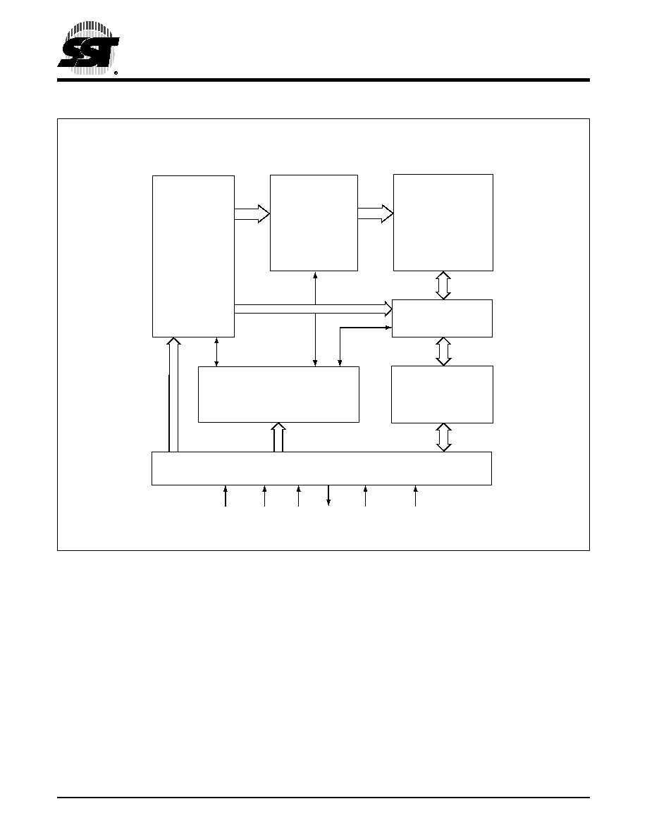
I/O Buffers
and
Data Latches
SuperFlash
Memory
X - Decoder
Control Logic
Address
Buffers
and
Latches
CE#
Y - Decoder
SCK
SI
SO
WP#
HOLD#
Serial Interface
F
UNCTIONAL
B
LOCK
D
IAGRAM

Data Sheet
2 Mbit / 4 Mbit SPI Serial Flash
SST25VF020 / SST25VF040
3
©2004 Silicon Storage Technology, Inc.
S71231-04-000
6/04
PIN DESCRIPTION
FIGURE 1: P
IN
A
SSIGNMENTS
TABLE
1: P
IN
D
ESCRIPTION
Symbol
Pin Name
Functions
SCK
Serial Clock
To provide the timing of the serial interface.
Commands, addresses, or input data are latched on the rising edge of the clock input, while output
data is shifted out on the falling edge of the clock input.
SI
Serial Data
Input
To transfer commands, addresses, or data serially into the device.
Inputs are latched on the rising edge of the serial clock.
SO
Serial Data
Output
To transfer data serially out of the device.
Data is shifted out on the falling edge of the serial clock.
CE#
Chip Enable
The device is enabled by a high to low transition on CE#. CE# must remain low for the duration of
any command sequence.
WP#
Write Protect
The Write Protect (WP#) pin is used to enable/disable BPL bit in the status register.
HOLD#
Hold
To temporarily stop serial communication with SPI flash memory without resetting the device.
V
DD
Power Supply
To provide power supply (2.7-3.6V).
V
SS
Ground
T1.0 1231
8-
LEAD
SOIC
8-
CONTACT
WSON
1
2
3
4
8
7
6
5
CE#
SO
WP#
VSS
Top View
VDD
HOLD#
SCK
SI
1231 08-wson P2.0
1
2
3
4
8
7
6
5
CE#
SO
WP#
VSS
VDD
HOLD#
SCK
SI
Top View
1231 08-soic P1.0

4
Data Sheet
2 Mbit / 4 Mbit SPI Serial Flash
SST25VF020 / SST25VF040
©2004 Silicon Storage Technology, Inc.
S71231-04-000
6/04
PRODUCT IDENTIFICATION
MEMORY ORGANIZATION
The SST25VF020/040 SuperFlash memory array is orga-
nized in 4 KByte sectors with 32 KByte overlay blocks.
DEVICE OPERATION
The SST25VF020/040 is accessed through the SPI (Serial
Peripheral Interface) bus compatible protocol. The SPI bus
consist of four control lines; Chip Enable (CE#) is used to
select the device, and data is accessed through the Serial
Data Input (SI), Serial Data Output (SO), and Serial Clock
(SCK).
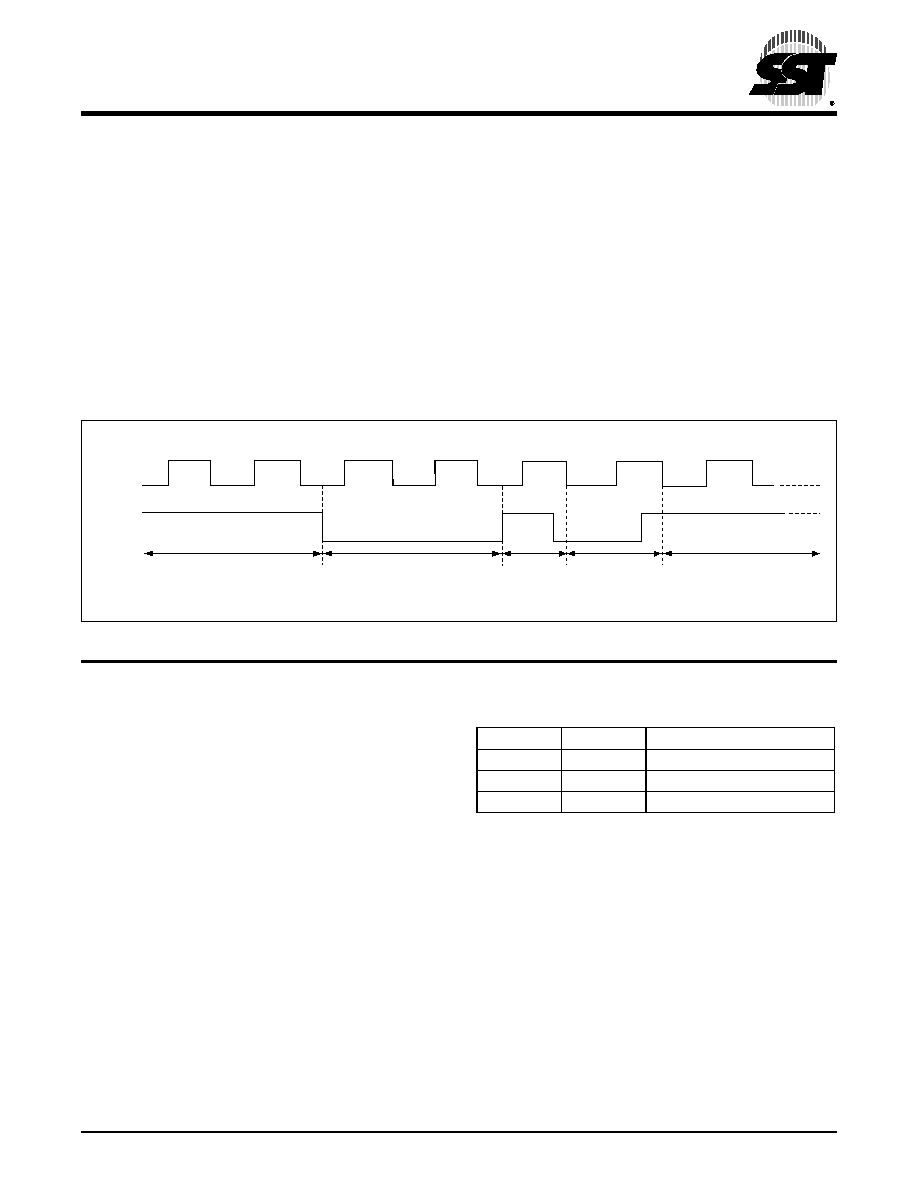
The SST25VF020/040 supports both Mode 0 (0,0) and
Mode 3 (1,1) of SPI bus operations. The difference
between the two modes, as shown in Figure 2, is the state
of the SCK signal when the bus master is in Stand-by
mode and no data is being transferred. The SCK signal is
low for Mode 0 and SCK signal is high for Mode 3. For both
modes, the Serial Data In (SI) is sampled at the rising edge
of the SCK clock signal and the Serial Data Output (SO) is
driven after the falling edge of the SCK clock signal.
FIGURE 2: SPI P
ROTOCOL
TABLE
2: P
RODUCT
I
DENTIFICATION
Address
Data
Manufacturer's ID
00000H
BFH
Device ID
SST25VF020
00001H
43H
SST25VF040
00001H
44H
T2.0 1231
1231 F02.1
MODE 3
SCK
SI
SO
CE#
MODE 3
DON'T CARE
Bit 7 Bit 6 Bit 5 Bit 4 Bit 3 Bit 2 Bit 1 Bit 0
Bit 7 Bit 6 Bit 5 Bit 4 Bit 3 Bit 2 Bit 1 Bit 0
MODE 0
MODE 0
HIGH IMPEDANCE
MSB
MSB
Data Sheet
2 Mbit / 4 Mbit SPI Serial Flash
SST25VF020 / SST25VF040
5
©2004 Silicon Storage Technology, Inc.
S71231-04-000
6/04
Hold Operation
HOLD# pin is used to pause a serial sequence underway
with the SPI flash memory without resetting the clocking
sequence. To activate the HOLD# mode, CE# must be in
active low state. The HOLD# mode begins when the SCK
active low state coincides with the falling edge of the
HOLD# signal. The HOLD mode ends when the HOLD#
signal's rising edge coincides with the SCK active low state.
If the falling edge of the HOLD# signal does not coincide
with the SCK active low state, then the device enters Hold
mode when the SCK next reaches the active low state.
Similarly, if the rising edge of the HOLD# signal does not
coincide with the SCK active low state, then the device
exits in Hold mode when the SCK next reaches the active
low state. See Figure 3 for Hold Condition waveform.
Once the device enters Hold mode, SO will be in high-
impedance state while SI and SCK can be V
IL
or V
IH
.
If CE# is driven active high during a Hold condition, it resets
the internal logic of the device. As long as HOLD# signal is
low, the memory remains in the Hold condition. To resume
communication with the device, HOLD# must be driven
active high, and CE# must be driven active low. See Figure
17 for Hold timing.
FIGURE 3: H
OLD
C
ONDITION
W
AVEFORM
Write Protection
SST25VF020/040 provides software Write protection. The
Write Protect pin (WP#) enables or disables the lock-down
function of the status register. The Block-Protection bits
(BP1, BP0, and BPL) in the status register provide Write
protection to the memory array and the status register. See
Table 5 for Block-Protection description.
Write Protect Pin (WP#)
The Write Protect (WP#) pin enables the lock-down func-
tion of the BPL bit (bit 7) in the status register. When WP#
is driven low, the execution of the Write-Status-Register
(WRSR) instruction is determined by the value of the BPL
bit (see Table 3). When WP# is high, the lock-down func-
tion of the BPL bit is disabled.
Active
Hold
Active
Hold
Active
1231 F03.0
SCK
HOLD#
TABLE
3: C
ONDITIONS
TO
EXECUTE
W
RITE
-S
TATUS
-
R
EGISTER
(WRSR) I
NSTRUCTION
WP#
BPL
Execute WRSR Instruction
L
1
Not Allowed
L
0
Allowed
H
X
Allowed
T3.0 1231