
©2003 Silicon Storage Technology, Inc.
S71250-00-000
10/03
1
The SST logo and SuperFlash are registered Trademarks of Silicon Storage Technology, Inc.
These specifications are subject to change without notice.
Advance Information
FEATURES:
∑
Single Voltage Read and Write Operations
≠ 2.7-3.6V for SST25VF080
∑
Serial Interface Architecture
≠ SPI Compatible: Mode 0 and Mode 3
∑
33 MHz Max Clock Frequency
∑
Superior Reliability
≠ Endurance: 100,000 Cycles (typical)
≠ Greater than 100 years Data Retention
∑
Low Power Consumption:
≠ Active Read Current: 7 mA (typical)
≠ Standby Current: 8 µA (typical)
∑
Flexible Erase Capability
≠ Uniform 4 KByte sectors
≠ Uniform 32 KByte overlay blocks
∑
Fast Erase and Byte-Program:
≠ Chip-Erase Time: 70 ms (typical)
≠ Sector- or Block-Erase Time: 18 ms (typical)
≠ Byte-Program Time: 14 µs (typical)
∑
Auto Address Increment (AAI) Programming
≠ Decrease total chip programming time over
Byte-Program operations
∑
End-of-Write Detection
≠ Software Status
∑
Hold Pin (HOLD#)
≠ Suspends a serial sequence to the memory
without deselecting the device
∑
Write Protection (WP#)
≠ Enables/Disables the Lock-Down function of the
status register
∑
Software Write Protection
≠ Write protection through Block-Protection bits in
status register
∑
Temperature Range
≠ Commercial: 0∞C to +70∞C
≠ Industrial: -40∞C to +85∞C
∑
Packages Available
≠ 8-lead SOIC 200 mil body width
PRODUCT DESCRIPTION
SST's serial flash family features a four-wire, SPI-com-
patible interface that allows for a low pin-count package
occupying less board space and ultimately lowering total
system costs. SST25VF080 SPI serial flash memories
are manufactured with SST's proprietary, high perfor-
mance CMOS SuperFlash technology. The split-gate cell
design and thick-oxide tunneling injector attain better reli-
ability and manufacturability compared with alternate
approaches.
The SST25VF080 devices significantly improve perfor-
mance, while lowering power consumption. The total
energy consumed is a function of the applied voltage,
current, and time of application. Since for any given volt-
age range, the SuperFlash technology uses less current
to program and has a shorter erase time, the total energy
consumed during any Erase or Program operation is less
than alternative flash memory technologies. The
SST25VF080 devices operate with a single 2.7-3.6V
power supply.
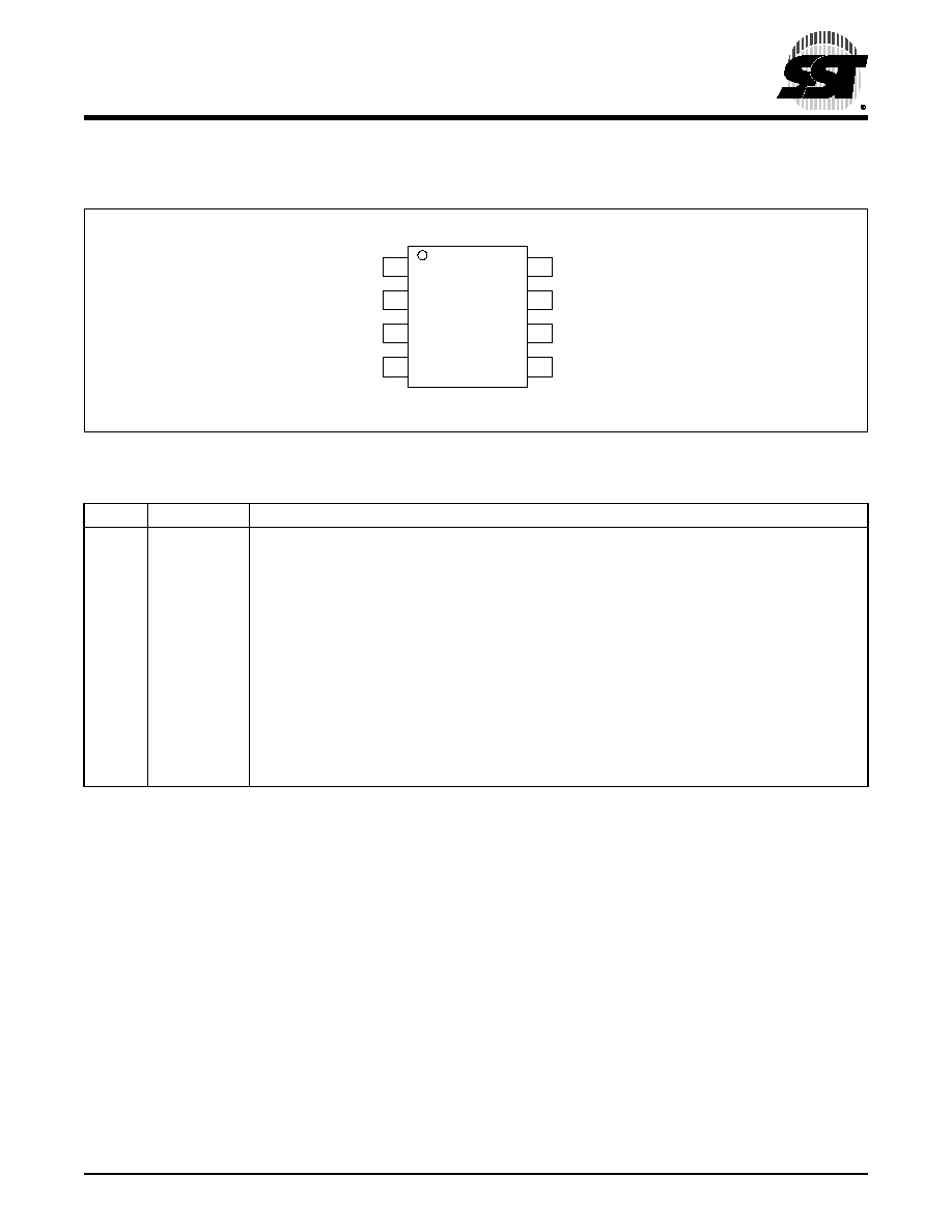
The SST25VF080 devices are offered in an 8-lead SOIC
package with 200 mil body width. See Figure 1 for pin
assignments.
8 Mbit SPI Serial Flash
SST25VF080
SST25VF0808 Mb Serial Peripheral Interface (SPI) flash memory
2
Advance Information
8 Mbit SPI Serial Flash
SST25VF080
©2003 Silicon Storage Technology, Inc.
S71250-00-000
10/03
1250 B1.0
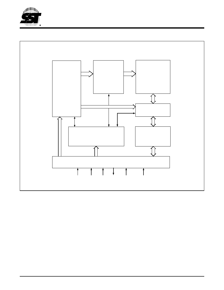
I/O Buffers
and
Data Latches
SuperFlash
Memory
X - Decoder
Control Logic
Address
Buffers
and
Latches
CE#
Y - Decoder
SCK
SI
SO
WP#
HOLD#
Serial Interface
F
UNCTIONAL
B
LOCK
D
IAGRAM
Advance Information
8 Mbit SPI Serial Flash
SST25VF080
3
©2003 Silicon Storage Technology, Inc.
S71250-00-000
10/03
PIN DESCRIPTION
FIGURE 1: P
IN
A
SSIGNMENTS
FOR
8-
LEAD
SOIC
TABLE
1: P
IN
D
ESCRIPTION
Symbol
Pin Name
Functions
SCK
Serial Clock
To provide the timing of the serial interface.
Commands, addresses, or input data are latched on the rising edge of the clock input, while output
data is shifted out on the falling edge of the clock input.
SI
Serial Data
Input
To transfer commands, addresses, or data serially into the device.
Inputs are latched on the rising edge of the serial clock.
SO
Serial Data
Output
To transfer data serially out of the device.
Data is shifted out on the falling edge of the serial clock.
CE#
Chip Enable
The device is enabled by a high to low transition on CE#. CE# must remain low for the duration of
any command sequence.
WP#
Write Protect
The Write Protect (WP#) pin is used to enable/disable BPL bit in the status register.
HOLD#
Hold
To temporarily stop serial communication with SPI flash memory without resetting the device.
V
DD
Power Supply
To provide power supply voltage: 2.7-3.6V for SST25VF080
V
SS
Ground
T1.0 1250
1
2
3
4
8
7
6
5
CE#
SO
WP#
VSS
VDD
HOLD#
SCK
SI
Top View
1250 08-soic P1.0

4
Advance Information
8 Mbit SPI Serial Flash
SST25VF080
©2003 Silicon Storage Technology, Inc.
S71250-00-000
10/03
PRODUCT IDENTIFICATION
MEMORY ORGANIZATION
The SST25VF080 SuperFlash memory array is organized
in 4 KByte sectors with 32 KByte overlay blocks.
DEVICE OPERATION
The SST25VF080 is accessed through the SPI (Serial
Peripheral Interface) bus compatible protocol. The SPI bus
consist of four control lines; Chip Enable (CE#) is used to
select the device, and data is accessed through the Serial
Data Input (SI), Serial Data Output (SO), and Serial Clock
(SCK).
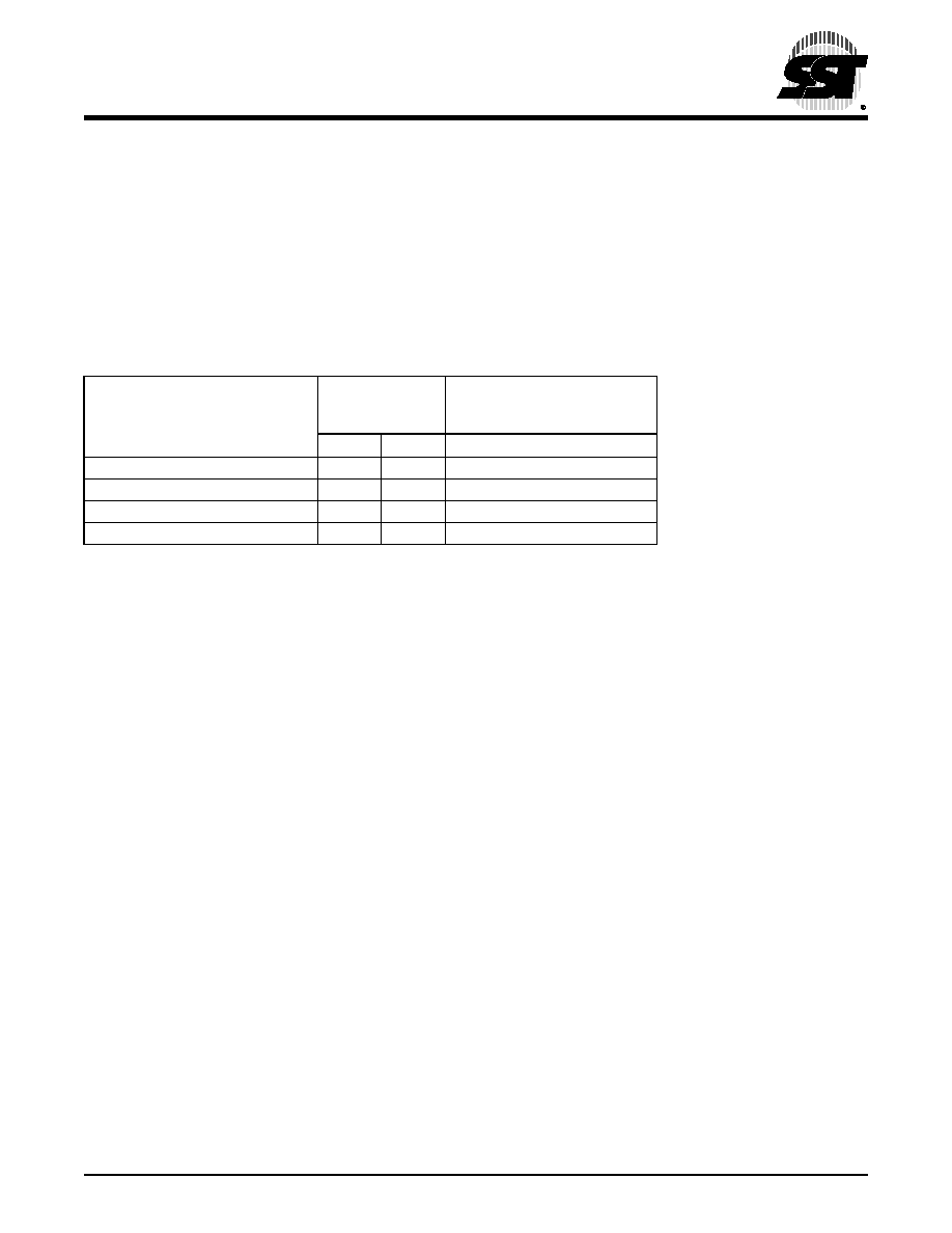
The SST25VF080 supports both Mode 0 (0,0) and Mode 3
(1,1) of SPI bus operations. The difference between the
two modes, as shown in Figure 2, is the state of the SCK
signal when the bus master is in Stand-by mode and no
data is being transferred. The SCK signal is low for Mode 0
and SCK signal is high for Mode 3. For both modes, the
Serial Data In (SI) is sampled at the rising edge of the SCK
clock signal and the Serial Data Output (SO) is driven after
the falling edge of the SCK clock signal.
FIGURE 2: SPI P
ROTOCOL
TABLE
2: P
RODUCT
I
DENTIFICATION
Address
Data
Manufacturer's ID
00000H
BFH
Device ID
SST25VF080
00001H
80H
T2.0 1250
1250 F02.0
MODE 3
SCK
SI
SO
CE#
MODE 3
DON'T CARE
Bit 7 Bit 6 Bit 5 Bit 4 Bit 3 Bit 2 Bit 1 Bit 0
Bit 7 Bit 6 Bit 5 Bit 4 Bit 3 Bit 2 Bit 1 Bit 0
MODE 0
MODE 0
HIGH IMPEDANCE
MSB
MSB
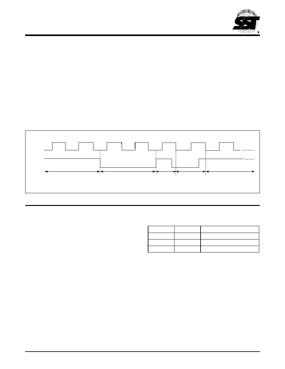
Advance Information
8 Mbit SPI Serial Flash
SST25VF080
5
©2003 Silicon Storage Technology, Inc.
S71250-00-000
10/03
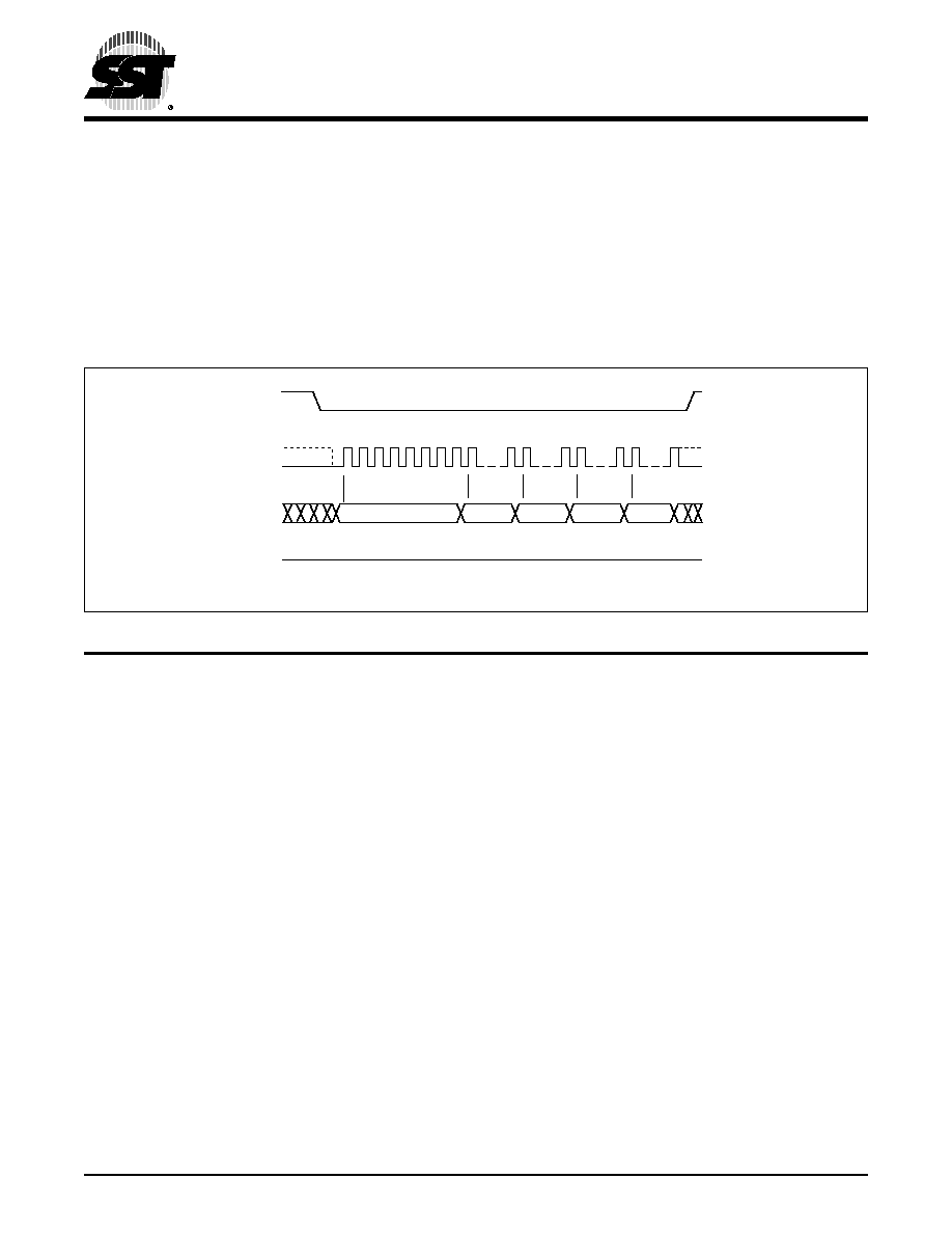
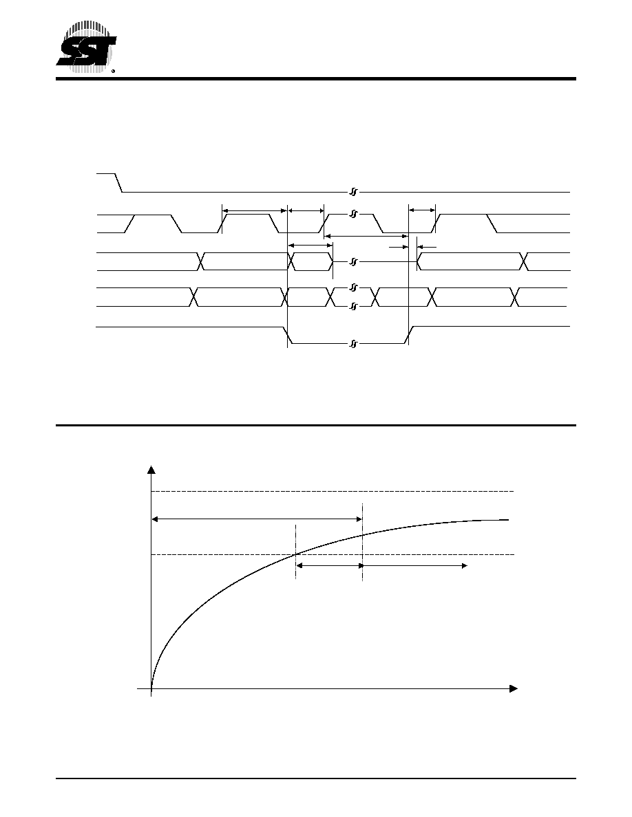
Hold Operation
HOLD# pin is used to pause a serial sequence underway
with the SPI flash memory without resetting the clocking
sequence. To activate the HOLD# mode, CE# must be in
active low state. The HOLD# mode begins when the SCK
active low state coincides with the falling edge of the
HOLD# signal. The HOLD mode ends when the HOLD#
signal's rising edge coincides with the SCK active low state.
If the falling edge of the HOLD# signal does not coincide
with the SCK active low state, then the device enters Hold
mode when the SCK next reaches the active low state.
Similarly, if the rising edge of the HOLD# signal does not
coincide with the SCK active low state, then the device
exits in Hold mode when the SCK next reaches the active
low state. See Figure 3 for Hold Condition waveform.
Once the device enters Hold mode, SO will be in high-
impedance state while SI and SCK can be V
IL
or V
IH
.
If CE# is driven active high during a Hold condition, it resets
the internal logic of the device. As long as HOLD# signal is
low, the memory remains in the Hold condition. To resume
communication with the device, HOLD# must be driven
active high, and CE# must be driven active low. See Figure
17 for Hold timing.
FIGURE 3: H
OLD
C
ONDITION
W
AVEFORM
Write Protection
SST25VF080 provides software Write protection. The
Write Protect pin (WP#) enables or disables the lock-down
function of the status register. The Block-Protection bits
(BP1, BP0, and BPL) in the status register provide Write
protection to the memory array and the status register. See
Table 5 for Block-Protection description.
Write Protect Pin (WP#)
The Write Protect (WP#) pin enables the lock-down func-
tion of the BPL bit (bit 7) in the status register. When WP#
is driven low, the execution of the Write-Status-Register
(WRSR) instruction is determined by the value of the BPL
bit (see Table 3). When WP# is high, the lock-down func-
tion of the BPL bit is disabled.
Active
Hold
Active
Hold
Active
1250 F03.0
SCK
HOLD#
TABLE
3: C
ONDITIONS
TO
EXECUTE
W
RITE
-S
TATUS
-
R
EGISTER
(WRSR) I
NSTRUCTION
WP#
BPL
Execute WRSR Instruction
L
1
Not Allowed
L
0
Allowed
H
X
Allowed
T3.0 1250
6
Advance Information
8 Mbit SPI Serial Flash
SST25VF080
©2003 Silicon Storage Technology, Inc.
S71250-00-000
10/03
Status Register
The software status register provides status on whether the
flash memory array is available for any Read or Write oper-
ation, whether the device is Write enabled, and the state of
the memory Write protection. During an internal Erase or
Program operation, the status register may be read only to
determine the completion of an operation in progress.
Table 4 describes the function of each bit in the software
status register.
Busy
The Busy bit determines whether there is an internal Erase
or Program operation in progress. A "1" for the Busy bit indi-
cates the device is busy with an operation in progress. A "0"
indicates the device is ready for the next valid operation.
Write Enable Latch (WEL)
The Write-Enable-Latch bit indicates the status of the inter-
nal memory Write Enable Latch. If the Write-Enable-Latch
bit is set to "1", it indicates the device is Write enabled. If the
bit is set to "0" (reset), it indicates the device is not Write
enabled and does not accept any memory Write (Program/
Erase) commands. The Write-Enable-Latch bit is automati-
cally reset under the following conditions:
∑
Power-up
∑
Write-Disable (WRDI) instruction completion
∑
Byte-Program instruction completion
∑
Auto Address Increment (AAI) programming
reached its highest memory address
∑
Sector-Erase instruction completion
∑
Block-Erase instruction completion
∑
Chip-Erase instruction completion
TABLE
4: S
OFTWARE
S
TATUS
R
EGISTER
Bit
Name
Function
Default at
Power-up
Read/Write
0
BUSY
1 = Internal Write operation is in progress
0 = No internal Write operation is in progress
0
R
1
WEL
1 = Device is memory Write enabled
0 = Device is not memory Write enabled
0
R
2
BP0
Indicate current level of block write protection (See Table 5)
1
R/W
3
BP1
Indicate current level of block write protection (See Table 5)
1
R/W
4:5
RES
Reserved for future use
0
N/A
6
AAI
Auto Address Increment Programming status
1 = AAI programming mode
0 = Byte-Program mode
0
R
7
BPL
1 = BP1, BP0 are read-only bits
0 = BP1, BP0 are read/writable
0
R/W
T4.0 1250
Advance Information
8 Mbit SPI Serial Flash
SST25VF080
7
©2003 Silicon Storage Technology, Inc.
S71250-00-000
10/03
Block Protection (BP1, BP0)
The Block-Protection (BP1, BP0) bits define the size of the
memory area, as defined in Table 5, to be software pro-
tected against any memory Write (Program or Erase)
operations. The Write-Status-Register (WRSR) instruction
is used to program the BP1 and BP0 bits as long as WP#
is high or the Block-Protect-Lock (BPL) bit is 0. Chip-Erase
can only be executed if Block-Protection bits are both 0.
After power-up, BP1 and BP0 are set to 1.
Block Protection Lock-Down (BPL)
WP# pin driven low (V
IL
), enables the Block-Protection-
Lock-Down (BPL) bit. When BPL is set to 1, it prevents any
further alteration of the BPL, BP1, and BP0 bits. When the
WP# pin is driven high (V
IH
), the BPL bit has no effect and
its value is "Don't Care". After power-up, the BPL bit is
reset to 0.
Auto Address Increment (AAI)
The Auto Address Increment Programming-Status bit pro-
vides status on whether the device is in AAI programming
mode or Byte-Program mode. The default at power up is
Byte-Program mode.
TABLE
5: S
OFTWARE
S
TATUS
R
EGISTER
B
LOCK
P
ROTECTION1
1. Default at power-up for BP1 and BP0 is `11'.
Protection Level
Status
Register
Bit
Protected Memory Area
BP1
BP0
8 Mbit
0
0
0
None
1 (1/4 Memory Array)
0
1
0C0000H-0FFFFFH
2 (1/2 Memory Array)
1
0
080000H-0FFFFFH
3 (Full Memory Array)
1
1
000000H-0FFFFFH
T5.0 1250

8
Advance Information
8 Mbit SPI Serial Flash
SST25VF080
©2003 Silicon Storage Technology, Inc.
S71250-00-000
10/03
Instructions
Instructions are used to Read, Write (Erase and Program),
and configure the SST25VF080. The instruction bus
cycles are 8 bits each for commands (Op Code), data, and
addresses. Prior to executing any Byte-Program, Auto
Address Increment (AAI) programming, Sector-Erase,
Block-Erase, or Chip-Erase instructions, the Write-Enable
(WREN) instruction must be executed first. The complete
list of the instructions is provided in Table 6. All instructions
are synchronized off a high to low transition of CE#. Inputs
will be accepted on the rising edge of SCK starting with the
most significant bit. CE# must be driven low before an
instruction is entered and must be driven high after the last
bit of the instruction has been shifted in (except for Read,
Read-ID and Read-Status-Register instructions). Any low
to high transition on CE#, before receiving the last bit of an
instruction bus cycle, will terminate the instruction in
progress and return the device to the standby mode.
Instruction commands (Op Code), addresses, and data are
all input from the most significant bit (MSB) first.
TABLE
6: D
EVICE
O
PERATION
I
NSTRUCTIONS1
1. A
MS
= Most Significant Address
A
MS
= A
19
for SST25VF080
Address bits above the most significant bit of each density can be V
IL
or V
IH
Cycle Type/
Operation
2,3
2. Operation: S
IN
= Serial In, S
OUT
= Serial Out
3. X = Dummy Input Cycles (V
IL
or V
IH
);
- = Non-Applicable Cycles (Cycles are not necessary)
Bus Cycle
4
4. One bus cycle is eight clock periods.
1
2
3
4
5
6
S
IN
S
OUT
S
IN
S
OUT
S
IN
S
OUT
S
IN
S
OUT
S
IN
S
OUT
S
IN
S
OUT
Read
03H
Hi-Z
A
23
-A
16
Hi-Z
A
15
-A
8
Hi-Z
A
7
-A
0
Hi-Z
X
D
OUT
Sector-Erase
5,6
5. Sector addresses: use A
MS
-A
12
, remaining addresses can be V
IL
or V
IH
6. Prior to any Byte-Program, AAI-Program, Sector-Erase, Block-Erase, or Chip-Erase operation, the Write-Enable (WREN) instruction
must be executed.
20H
Hi-Z
A
23
-A
16
Hi-Z
A
15
-A
8
Hi-Z
A
7
-A
0
Hi-Z
-
-
Block-Erase
5,7
7. Block addresses for: use A
MS
-A
15
, remaining addresses can be V
IL
or V
IH
52H
Hi-Z
A
23
-A
16
Hi-Z
A
15
-A
8
Hi-Z
A
7
-A
0
Hi-Z
-
-
Chip-Erase
6
60H
Hi-Z
-
-
-
-
-
-
-
-
Byte-Program
6
02H
Hi-Z
A
23
-A
16
Hi-Z
A
15
-A
8
Hi-Z
A
7
-A
0
Hi-Z
D
IN
Hi-Z
Auto Address Increment
(AAI) Single-Byte Program
6,8
8. To continue programming to the next sequential address location, enter the 8-bit command, AFH,
followed by the data to be programmed.
AFH
Hi-Z
A
23
-A
16
Hi-Z
A
15
-A
8
Hi-Z
A
7
-A
0
Hi-Z
D
IN
Hi-Z
Read-Status-Register
(RDSR)
05H
Hi-Z
X
D
OUT
-
Note
9
9. The Read-Status-Register is continuous with ongoing clock cycles until terminated by a low to high transition on CE#.
-
Note
9
-
Note
9
Enable-Write-Status-Register
(EWSR)
10
10. The Enable-Write-Status-Register (EWSR) instruction and the Write-Status-Register (WRSR) instruction must work in conjunction of
each other. The WRSR instruction must be executed immediately (very next bus cycle) after the EWSR instruction to make both
instructions effective.
50H
Hi-Z
-
-
-
-
-
-
-
-
Write-Status-Register
(WRSR)
10
01H
Hi-Z
Data
Hi-Z
-
-
-.
-
-
-
Write-Enable (WREN)
06H
Hi-Z
-
-
-
-
-
-
-
-
Write-Disable (WRDI)
04H
Hi-Z
-
-
-
-
-
-
-
-
Read-ID
90H or
ABH
Hi-Z
00H
Hi-Z
00H
Hi-Z
ID
Addr
11
11. Manufacturer's ID is read with A
0
=0, and Device ID is read with A
0
=1. All other address bits are 00H. The Manufacturer and Device
ID output stream is continuous until terminated by a low to high transition on CE#
Hi-Z
X
D
OUT
12
12. Device ID = 80H for SST25VF080
T6.0 1250

Advance Information
8 Mbit SPI Serial Flash
SST25VF080
9
©2003 Silicon Storage Technology, Inc.
S71250-00-000
10/03
Read
The Read instruction supports up to 20 MHz, it outputs the
data starting from the specified address location. The data
output stream is continuous through all addresses until ter-
minated by a low to high transition on CE#. The internal
address pointer will automatically increment until the high-
est memory address is reached. Once the highest memory
address is reached, the address pointer will automatically
increment to the beginning (wrap-around) of the address
space, i.e. for 8 Mbit density, once the data from address
location 0FFFFFH had been read, the next output will be
from address location 000000H.
The Read instruction is initiated by executing an 8-bit com-
mand, 03H, followed by address bits [A
23
-A
0
]. CE# must
remain active low for the duration of the Read cycle. See
Figure 4 for the Read sequence.
FIGURE 4: R
EAD
S
EQUENCE
1250 F04.0
CE#
SO
SI
SCK
ADD.
0 1 2 3 4 5 6 7 8
ADD.
ADD.
03
HIGH IMPEDANCE
15 16
23 24
31 32
39 40
70
47
48
55 56
63 64
N+2
N+3
N+4
N
N+1
D
OUT
MSB
MSB
MSB
MODE 0
MODE 3
D
OUT
D
OUT
D
OUT
D
OUT
10
Advance Information
8 Mbit SPI Serial Flash
SST25VF080
©2003 Silicon Storage Technology, Inc.
S71250-00-000
10/03
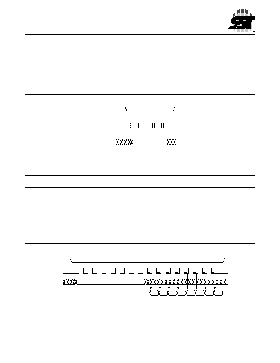
Byte-Program
The Byte-Program instruction programs the bits in the
selected byte to the desired data. The selected byte must
be in the erased state (FFH) when initiating a Program
operation. A Byte-Program instruction applied to a pro-
tected memory area will be ignored.
Prior to any Write operation, the Write-Enable (WREN)
instruction must be executed. CE# must remain active low
for the duration of the Byte-Program instruction. The Byte-
Program instruction is initiated by executing an 8-bit com-
mand, 02H, followed by address bits [A
23
-A
0
]. Following the
address, the data is input in order from MSB (bit 7) to LSB
(bit 0). CE# must be driven high before the instruction is
executed. The user may poll the Busy bit in the software
status register or wait T
BP
for the completion of the internal
self-timed Byte-Program operation. See Figure 5 for the
Byte-Program sequence.
FIGURE 5: B
YTE
-P
ROGRAM
S
EQUENCE
1250 F05.0
CE#
SO
SI
SCK
ADD.
0 1 2 3 4 5 6 7 8
ADD.
ADD.
D
IN
02
HIGH IMPEDANCE
15 16
23 24
31 32
39
MODE 0
MODE 3
MSB
MSB
MSB
LSB
Advance Information
8 Mbit SPI Serial Flash
SST25VF080
11
©2003 Silicon Storage Technology, Inc.
S71250-00-000
10/03
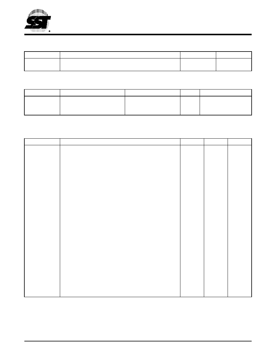
Auto Address Increment (AAI) Program
The AAI program instruction allows multiple bytes of data to
be programmed without re-issuing the next sequential
address location. This feature decreases total program-
ming time when the entire memory array is to be pro-
grammed. An AAI program instruction pointing to a
protected memory area will be ignored. The selected
address range must be in the erased state (FFH) when ini-
tiating an AAI program instruction.
Prior to any write operation, the Write-Enable (WREN)
instruction must be executed. The AAI program instruction
is initiated by executing an 8-bit command, AFH, followed
by address bits [A
23
-A
0
]. Following the addresses, the data
is input sequentially from MSB (Bit 7) to LSB (Bit 0). CE#
must be driven high before the AAI program instruction is
executed. The user must poll the BUSY bit in the software
status register or wait T
BP
for the completion of each inter-
nal self-timed Byte-Program cycle. Once the device com-
pletes programming byte, the next sequential address may
be program, enter the 8-bit command, AFH, followed by the
data to be programmed. When the last desired byte had
been programmed, execute the Write-Disable (WRDI)
instruction, 04H, to terminate AAI. After execution of the
WRDI command, the user must poll the Status register to
ensure the device completes programming. See Figure 6
for AAI programming sequence.
There is no wrap mode during AAI programming; once the
highest unprotected memory address is reached, the
device will exit AAI operation and reset the Write-Enable-
Latch bit (WEL = 0).
FIGURE 6: A
UTO
A
DDRESS
I
NCREMENT
(AAI) P
ROGRAM
S
EQUENCE
CE#
SI
SCK
A[23:16] A[15:8]
A[7:0]
AF
Data Byte 1
AF
Data Byte 2
CE#
SI
SO
SCK
Write Disable (WRDI)
Instruction to terminate
AAI Operation
Read Status Register (RDSR)
Instruction to verify end of
AAI Operation
04
Last Data Byte
AF
05
D
OUT
MODE 3
MODE 0
T
BP
TBP
T
BP
1250 F06.0
0 1 2 3 4 5 6 7 8
32 33 34 35 36 37 38 39
15 16
23 24
31
0 1 2 3 4 5 6 7 8 9 10 11 12 13 14 15
0 1
0 1 2 3 4 5 6 7
0 1 2 3 4 5 6 7 8 9 10 11 12 13 14 15
0 1 2 3 4 5 6 7 8 9 10 11 12 13 14 15

12
Advance Information
8 Mbit SPI Serial Flash
SST25VF080
©2003 Silicon Storage Technology, Inc.
S71250-00-000
10/03
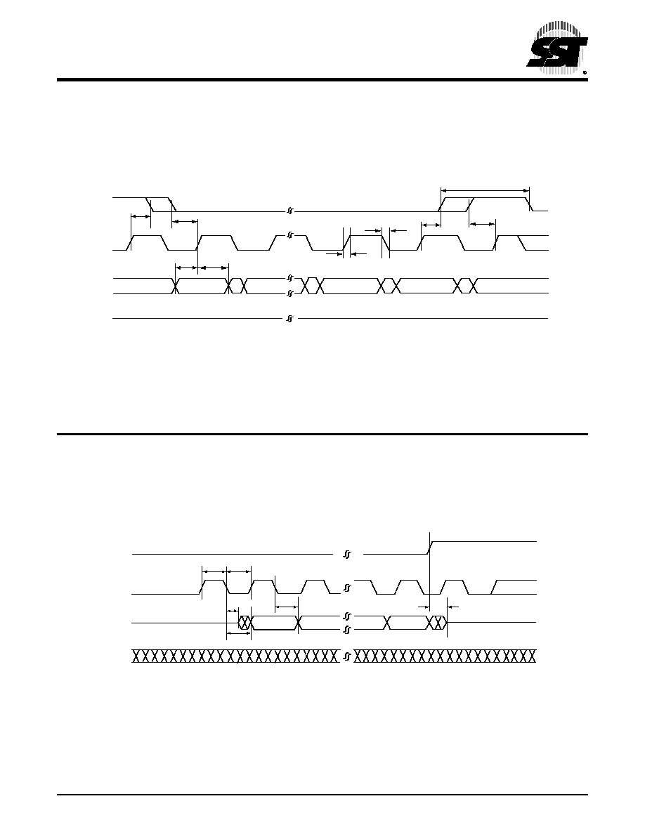
Sector-Erase
The Sector-Erase instruction clears all bits in the selected 4
KByte sector to FFH. A Sector-Erase instruction applied to
a protected memory area will be ignored. Prior to any Write
operation, the Write-Enable (WREN) instruction must be
executed. CE# must remain active low for the duration of
the any command sequence. The Sector-Erase instruction
is initiated by executing an 8-bit command, 20H, followed
by address bits [A
23
-A
0
]. Address bits [A
MS
-A
12
]
(A
MS
= Most Significant address) are used to determine the
sector address (SA
X
), remaining address bits can be V
IL
or
V
IH.
CE# must be driven high before the instruction is exe-
cuted. The user may poll the Busy bit in the software status
register or wait T
SE
for the completion of the internal self-
timed Sector-Erase cycle. See Figure 7 for the Sector-
Erase sequence.
FIGURE 7: S
ECTOR
-E
RASE
S
EQUENCE
Block-Erase
The Block-Erase instruction clears all bits in the selected 32
KByte block to FFH. A Block-Erase instruction applied to a
protected memory area will be ignored. Prior to any Write
operation, the Write-Enable (WREN) instruction must be
executed. CE# must remain active low for the duration of
any command sequence. The Block-Erase instruction is
initiated by executing an 8-bit command, 52H, followed by
address bits [A
23
-A
0
]. Address bits [A
MS
-A
15
] (A
MS
= Most
significant address) are used to determine block address
(BA
X
), remaining address bits can be V
IL
or V
IH
. CE# must
be driven high before the instruction is executed. The user
may poll the Busy bit in the software status register or wait
T
BE
for the completion of the internal self-timed Block-
Erase cycle. See Figure 8 for the Block-Erase sequence.
FIGURE 8: B
LOCK
-E
RASE
S
EQUENCE
CE#
SO
SI
SCK
ADD.
0 1 2 3 4 5 6 7 8
ADD.
ADD.
20
HIGH IMPEDANCE
15 16
23 24
31
MODE 0
MODE 3
1250 F07.0
MSB
MSB
CE#
SO
SI
SCK
ADD.
0 1 2 3 4 5 6 7 8
ADD.
ADD.
52
HIGH IMPEDANCE
15 16
23 24
31
MODE 0
MODE 3
1250 F08.0
MSB
MSB
Advance Information
8 Mbit SPI Serial Flash
SST25VF080
13
©2003 Silicon Storage Technology, Inc.
S71250-00-000
10/03
Chip-Erase
The Chip-Erase instruction clears all bits in the device to
FFH. A Chip-Erase instruction will be ignored if any of the
memory area is protected. Prior to any Write operation, the
Write-Enable (WREN) instruction must be executed. CE#
must remain active low for the duration of the Chip-Erase
instruction sequence. The Chip-Erase instruction is initiated
by executing an 8-bit command, 60H. CE# must be driven
high before the instruction is executed. The user may poll
the Busy bit in the software status register or wait T
CE
for
the completion of the internal self-timed Chip-Erase cycle.
See Figure 9 for the Chip-Erase sequence.
FIGURE 9: C
HIP
-E
RASE
S
EQUENCE
Read-Status-Register (RDSR)
The Read-Status-Register (RDSR) instruction allows read-
ing of the status register. The status register may be read at
any time even during a Write (Program/Erase) operation.
When a Write operation is in progress, the Busy bit may be
checked before sending any new commands to assure that
the new commands are properly received by the device.
CE# must be driven low before the RDSR instruction is
entered and remain low until the status data is read. Read-
Status-Register is continuous with ongoing clock cycles
until it is terminated by a low to high transition of the CE#.
See Figure 10 for the RDSR instruction sequence.
FIGURE 10: R
EAD
-S
TATUS
-R
EGISTER
(RDSR) S
EQUENCE
CE#
SO
SI
SCK
0 1 2 3 4 5 6 7
60
HIGH IMPEDANCE
MODE 0
MODE 3
1250 F09.0
MSB
0
1
2
3
4
5
6
7
8
9
10
11
12
13
14
1250 F10.0
MODE 3
SCK
SI
SO
CE#
Bit 7 Bit 6 Bit 5 Bit 4 Bit 3 Bit 2 Bit 1 Bit 0
05
MODE 0
HIGH IMPEDANCE
Status
Register Out
MSB
MSB
14
Advance Information
8 Mbit SPI Serial Flash
SST25VF080
©2003 Silicon Storage Technology, Inc.
S71250-00-000
10/03
Write-Enable (WREN)
The Write-Enable (WREN) instruction sets the Write-
Enable-Latch bit to 1 allowing Write operations to occur.
The WREN instruction must be executed prior to any Write
(Program/Erase) operation. CE# must be driven high
before the WREN instruction is executed.
FIGURE 11: W
RITE
E
NABLE
(WREN) S
EQUENCE
Write-Disable (WRDI)
The Write-Disable (WRDI) instruction resets the Write-
Enable-Latch bit and AAI bit to 0 disabling any new Write
operations from occurring. CE# must be driven high before
the WRDI instruction is executed.
FIGURE 12: W
RITE
D
ISABLE
(WRDI) S
EQUENCE
Enable-Write-Status-Register (EWSR)
The Enable-Write-Status-Register (EWSR) instruction
arms the Write-Status-Register (WRSR) instruction and
opens the status register for alteration. The Enable-Write-
Status-Register instruction does not have any effect and
will be wasted, if it is not followed immediately by the Write-
Status-Register (WRSR) instruction. CE# must be driven
low before the EWSR instruction is entered and must be
driven high before the EWSR instruction is executed.
CE#
SO
SI
SCK
0 1 2 3 4 5 6 7
06
HIGH IMPEDANCE
MODE 0
MODE 3
1250 F11.0
MSB
CE#
SO
SI
SCK
0 1 2 3 4 5 6 7
04
HIGH IMPEDANCE
MODE 0
MODE 3
1250 F12.0
MSB
Advance Information
8 Mbit SPI Serial Flash
SST25VF080
15
©2003 Silicon Storage Technology, Inc.
S71250-00-000
10/03
Write-Status-Register (WRSR)
The Write-Status-Register instruction works in conjunction
with the Enable-Write-Status-Register (EWSR) instruction
to write new values to the BP1, BP0, and BPL bits of the
status register. The Write-Status-Register instruction must
be executed immediately after the execution of the Enable-
Write-Status-Register instruction (very next instruction bus
cycle). This two-step instruction sequence of the EWSR
instruction followed by the WRSR instruction works like
SDP (software data protection) command structure which
prevents any accidental alteration of the status register val-
ues. The Write-Status-Register instruction will be ignored
when WP# is low and BPL bit is set to "1". When the WP#
is low, the BPL bit can only be set from "0" to "1" to lock-
down the status register, but cannot be reset from "1" to "0".
When WP# is high, the lock-down function of the BPL bit is
disabled and the BPL, BP0, and BP1 bits in the status reg-
ister can all be changed. As long as BPL bit is set to 0 or
WP# pin is driven high (V
IH
) prior to the low-to-high transi-
tion of the CE# pin at the end of the WRSR instruction, the
BP0, BP1, and BPL bit in the status register can all be
altered by the WRSR instruction. In this case, a single
WRSR instruction can set the BPL bit to "1" to lock down
the status register as well as altering the BP0 and BP1 bit
at the same time. See Table 3 for a summary description of
WP# and BPL functions. CE# must be driven low before
the command sequence of the WRSR instruction is
entered and driven high before the WRSR instruction is
executed. See Figure 13 for EWSR and WRSR instruction
sequences.
FIGURE 13: E
NABLE
-W
RITE
-S
TATUS
-R
EGISTER
(EWSR)
AND
W
RITE
-S
TATUS
-R
EGISTER
(WRSR) S
EQUENCE
1250 F13.0
MODE 3
HIGH IMPEDANCE
MODE 0
STATUS
REGISTER IN
7 6 5 4 3 2 1 0
MSB
MSB
MSB
01
MODE 3
SCK
SI
SO
CE#
MODE 0
50
0 1 2 3 4 5 6 7
0 1 2 3 4 5 6 7 8 9 10 11 12 13 14 15
16
Advance Information
8 Mbit SPI Serial Flash
SST25VF080
©2003 Silicon Storage Technology, Inc.
S71250-00-000
10/03
Read-ID
The Read-ID instruction identifies the devices as
SST25VF080 and manufacturer as SST. The device infor-
mation can be read from executing an 8-bit command, 90H
or ABH, followed by address bits [A
23
-A
0
]. Following the
Read-ID instruction, the manufacturer's ID is located in
address 00000H and the device ID is located in address
00001H. Once the device is in Read-ID mode, the manu-
facturer's and device ID output data toggles between
address 00000H and 00001H until terminated by a low to
high transition on CE#.
FIGURE 14: R
EAD
-ID S
EQUENCE
1250 F14.0
CE#
SO
SI
SCK
00
0 1 2 3 4 5 6 7 8
00
ADD
1
90 or AB
HIGH IMPEDANCE
15 16
23 24
31 32
39 40
47 48
55 56
63
BF
Device ID
BF
Device ID
Note: The manufacturer's and device ID output stream is continuous until terminated by a low to high transition on CE#.
Device ID = 80H for SST25VF080
1. 00H will output the manfacturer's ID first and 01H will output device ID first before toggling between the two.
HIGH
IMPEDANCE
MODE 3
MODE 0
MSB
MSB
MSB
Advance Information
8 Mbit SPI Serial Flash
SST25VF080
17
©2003 Silicon Storage Technology, Inc.
S71250-00-000
10/03
ELECTRICAL SPECIFICATIONS
Absolute Maximum Stress Ratings (Applied conditions greater than those listed under "Absolute Maximum
Stress Ratings" may cause permanent damage to the device. This is a stress rating only and functional operation
of the device at these conditions or conditions greater than those defined in the operational sections of this data
sheet is not implied. Exposure to absolute maximum stress rating conditions may affect device reliability.)
Temperature Under Bias . . . . . . . . . . . . . . . . . . . . . . . . . . . . . . . . . . . . . . . . . . . . . . . . . . . . . . . . . -55∞C to +125∞C
Storage Temperature . . . . . . . . . . . . . . . . . . . . . . . . . . . . . . . . . . . . . . . . . . . . . . . . . . . . . . . . . . . . -65∞C to +150∞C
D. C. Voltage on Any Pin to Ground Potential . . . . . . . . . . . . . . . . . . . . . . . . . . . . . . . . . . . . . . . . -0.5V to V
DD
+0.5V
Transient Voltage (<20 ns) on Any Pin to Ground Potential . . . . . . . . . . . . . . . . . . . . . . . . . . . . . . -2.0V to V
DD
+2.0V
Package Power Dissipation Capability (Ta = 25∞C) . . . . . . . . . . . . . . . . . . . . . . . . . . . . . . . . . . . . . . . . . . . . . . 1.0W
Surface Mount Lead Soldering Temperature (3 Seconds) . . . . . . . . . . . . . . . . . . . . . . . . . . . . . . . . . . . . . . . . 240∞C
Output Short Circuit Current
1
. . . . . . . . . . . . . . . . . . . . . . . . . . . . . . . . . . . . . . . . . . . . . . . . . . . . . . . . . . . . . . 50 mA
1. Output shorted for no more than one second. No more than one output shorted at a time.
O
PERATING
R
ANGE
Range
Ambient Temp
V
DD
Commercial
0∞C to +70∞C
2.7-3.6V
Industrial
-40∞C to +85∞C
2.7-3.6V
AC C
ONDITIONS
OF
T
EST
Input Rise/Fall Time . . . . . . . . . . . . . . . 5 ns
Output Load . . . . . . . . . . . . . . . . . . . . . C
L
= 30 pF
See Figures 19 and 20
TABLE
7: DC O
PERATING
C
HARACTERISTICS
Symbol
Parameter
Limits
Test Conditions
Min
Max
Units
I
DDR
Read Current
10
mA
CE#=0.1 V
DD
/0.9 V
DD
@20 MHz, SO=open
I
DDW
Program and Erase Current
30
mA
CE#=V
DD
I
SB
Standby Current
15
µA
CE#=V
DD
, V
IN
=V
DD
or V
SS
I
LI
Input Leakage Current
1
µA
V
IN
=GND to V
DD
, V
DD
=V
DD
Max
I
LO
Output Leakage Current
1
µA
V
OUT
=GND to V
DD
, V
DD
=V
DD
Max
V
IL
Input Low Voltage
0.8
V
V
DD
=V
DD
Min
V
IH
Input High Voltage
0.7 V
DD
V
V
DD
=V
DD
Max
V
OL
Output Low Voltage
0.2
V
I
OL
=100 µA, V
DD
=V
DD
Min
V
OH
Output High Voltage
V
DD
-0.2
V
I
OH
=-100 µA, V
DD
=V
DD
Min
T7.0 1250
TABLE
8: R
ECOMMENDED
S
YSTEM
P
OWER
-
UP
T
IMINGS
Symbol
Parameter
Minimum
Units
T
PU-READ
1
1. This parameter is measured only for initial qualification and after a design or process change that could affect this parameter.
V
DD
Min to Read Operation
10
µs
T
PU-WRITE
1
V
DD
Min to Write Operation
10
µs
T8.0 1250
18
Advance Information
8 Mbit SPI Serial Flash
SST25VF080
©2003 Silicon Storage Technology, Inc.
S71250-00-000
10/03
TABLE
9: C
APACITANCE
(Ta = 25∞C, f=1 Mhz, other pins open)
Parameter
Description
Test Condition
Maximum
C
OUT
1
Output Pin Capacitance
V
OUT
= 0V
12 pF
C
IN
1
Input Capacitance
V
IN
= 0V
6 pF
T9.0 1250
1. This parameter is measured only for initial qualification and after a design or process change that could affect this parameter.
TABLE 10: R
ELIABILITY
C
HARACTERISTICS
Symbol
Parameter
Minimum Specification
Units
Test Method
N
END
1
1. This parameter is measured only for initial qualification and after a design or process change that could affect this parameter.
Endurance
10,000
Cycles
JEDEC Standard A117
T
DR
1
Data Retention
100
Years
JEDEC Standard A103
I
LTH
1
Latch Up
100 + I
DD
mA
JEDEC Standard 78
T10.0 1250
TABLE 11: AC O
PERATING
C
HARACTERISTICS
Symbol
Parameter
Min
Max
Units
F
CLK
Serial Clock Frequency
20
MHz
T
SCKH
Serial Clock High Time
20
ns
T
SCKL
Serial Clock Low Time
20
ns
T
CES
1
1. Relative to SCK.
CE# Active Setup Time
20
ns
T
CEH
1
CE# Active Hold Time
20
ns
T
CHS
1
CE# Not Active Setup Time
10
ns
T
CHH
1
CE# Not Active Hold Time
10
ns
T
CPH
CE# High Time
100
ns
T
CHZ
CE# High to High-Z Output
20
ns
T
CLZ
SCK Low to Low-Z Output
0
ns
T
DS
Data In Setup Time
5
ns
T
DH
Data In Hold Time
5
ns
T
HLS
HOLD# Low Setup Time
10
ns
T
HHS
HOLD# High Setup Time
10
ns
T
HLH
HOLD# Low Hold Time
15
ns
T
HHH
HOLD# High Hold Time
10
ns
T
HZ
HOLD# Low to High-Z Output
20
ns
T
LZ
HOLD# High to Low-Z Output
20
ns
T
OH
Output Hold from SCK Change
0
ns
T
V
Output Valid from SCK
20
ns
T
SE
Sector-Erase
25
ms
T
BE
Block-Erase
25
ms
T
SCE
Chip-Erase
100
ms
T
BP
Byte-Program
20
µs
T11.0 1250
Advance Information
8 Mbit SPI Serial Flash
SST25VF080
19
©2003 Silicon Storage Technology, Inc.
S71250-00-000
10/03
FIGURE 15: S
ERIAL
I
NPUT
T
IMING
D
IAGRAM
FIGURE 16: S
ERIAL
O
UTPUT
T
IMING
D
IAGRAM
HIGH-Z
HIGH-Z
CE#
SO
SI
SCK
MSB
LSB
T
DS
T
DH
T
CHH
T
CES
T
CEH
T
CHS
T
SCKR
T
SCKF
T
CPH
1250 F15.0
1250 F16.0
CE#
SI
SO
SCK
MSB
T
CLZ
T
V
T
SCKH
T
CHZ
T
OH
T
SCKL
LSB
20
Advance Information
8 Mbit SPI Serial Flash
SST25VF080
©2003 Silicon Storage Technology, Inc.
S71250-00-000
10/03
FIGURE 17: H
OLD
T
IMING
D
IAGRAM
FIGURE 18: P
OWER
-
UP
T
IMING
D
IAGRAM
T
HZ
T
LZ
T
HHH
T
HLS
T
HLH
T
HHS
1250 F17.0
HOLD#
CE#
SCK
SO
SI
Time
V
DD
Min
V
DD
Max
V
DD
Device fully accessible
T
PU-READ
T
PU-WRITE
Chip selection is not allowed.
All commands are rejected by the device.
1250 F18.0
Advance Information
8 Mbit SPI Serial Flash
SST25VF080
21
©2003 Silicon Storage Technology, Inc.
S71250-00-000
10/03
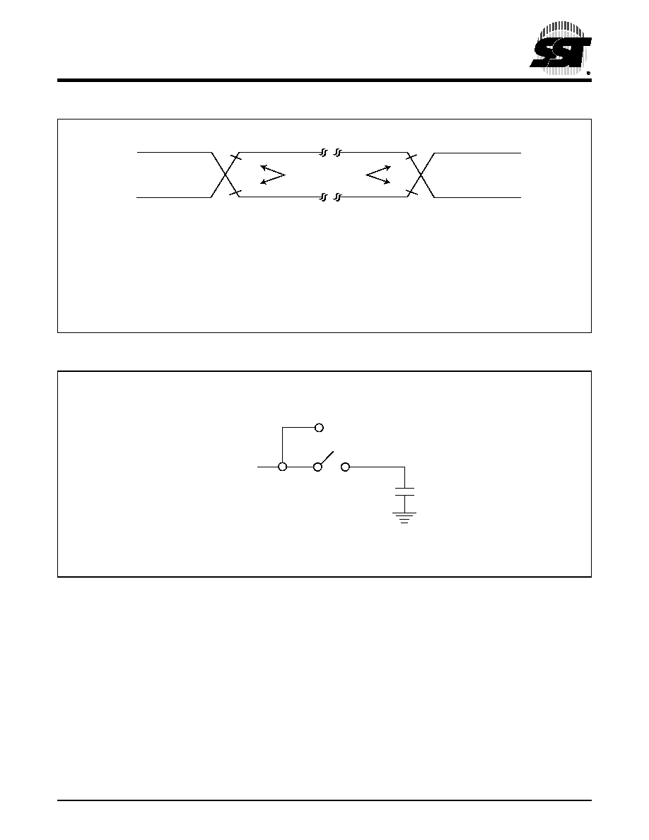
FIGURE 19: AC I
NPUT
/O
UTPUT
R
EFERENCE
W
AVEFORMS
FIGURE 20: A T
EST
L
OAD
E
XAMPLE
1250 F19.0
REFERENCE POINTS
OUTPUT
INPUT
VHT
VLT
VHT
VLT
VIHT
VILT
AC test inputs are driven at V
IHT
(0.9V
DD
) for a logic "1" and V
ILT
(0.1V
DD
) for a logic "0". Measurement reference points
for inputs and outputs are V
HT
(0.7V
DD
) and V
LT
(0.3V
DD
). Input rise and fall times (10%
90%) are <5 ns.
Note: V
HT
- V
HIGH
Test
V
LT
- V
LOW
Test
V
IHT
- V
INPUT
HIGH Test
V
ILT
- V
INPUT
LOW Test
1250 F20.0
TO TESTER
TO DUT
C
L
22
Advance Information
8 Mbit SPI Serial Flash
SST25VF080
©2003 Silicon Storage Technology, Inc.
S71250-00-000
10/03
PRODUCT ORDERING INFORMATION
Valid combinations for SST25VF080
SST25VF080-20-4C-S2A
SST25VF080-20-4C-S2AE
SST25VF080-20-4I-S2A
SST25VF080-20-4I-S2AE
Note: Valid combinations are those products in mass production or will be in mass production. Consult your SST sales
representative to confirm availability of valid combinations and to determine availability of new combinations.
SST
25
LF
080
-
33
- 4C -
SA
E
XX
XX XXXX X
- XXX
- XX -
XXX X
Environmental Attribute
E = non-Pb
Package Modifier
A = 8 leads or contacts
Package Type
S2 = SOIC 200 mil body width
Temperature Range
C = Commercial = 0∞C to +70∞C
I = Industrial = -40∞C to +85∞C
Minimum Endurance
4 = 10,000 cycles
Operating Frequency
20 = 20 MHz
Version
Device Density
080 = 8 Mbit
Voltage
V = 2.7-3.6V
Product Series
25 = SPI Serial Flash
Advance Information
8 Mbit SPI Serial Flash
SST25VF080
23
©2003 Silicon Storage Technology, Inc.
S71250-00-000
10/03
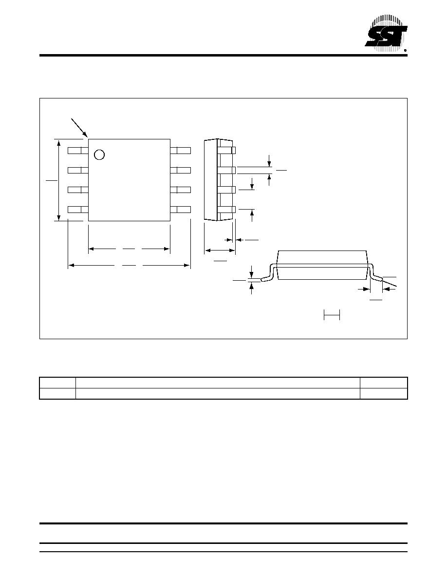
PACKAGING DIAGRAMS
8-
LEAD
S
MALL
O
UTLINE
I
NTEGRATED
C
IRCUIT
(SOIC) 200
MIL
BODY
WIDTH
(5.2
MM
X
8
MM
)
SST P
ACKAGE
C
ODE
: S2A
TABLE 12: R
EVISION
H
ISTORY
Number
Description
Date
00
∑
Initial release of data sheet
Oct 2003
08-soic-EIAJ-S2A-2
Note: 1. All linear dimensions are in millimeters (max/min).
2. Coplanarity: 0.1 mm
3. Maximum allowable mold flash is 0.15 mm at the package ends and 0.25 mm between leads.
TOP VIEW
SIDE VIEW
END VIEW
5.40
5.15
8.10
7.70
5.40
5.15
Pin #1
Identifier
0.50
0.35
1.27 BSC
0.25
0.05
2.20
1.75
0.25
0.19
0.80
0.50
0∞
8∞
1mm
Silicon Storage Technology, Inc. ∑ 1171 Sonora Court ∑ Sunnyvale, CA 94086 ∑ Telephone 408-735-9110 ∑ Fax 408-735-9036
www.SuperFlash.com or www.sst.com