©2003 Silicon Storage Technology, Inc.
S71134-03-000
8/03
1
The SST logo and SuperFlash are registered trademarks of Silicon Storage Technology, Inc.
ComboMemory is a trademark of Silicon Storage Technology, Inc.
These specifications are subject to change without notice.
Data Sheet
FEATURES:
∑
ROM + SRAM ROM/RAM Combo
≠ SST30VR041: 512K x8 ROM + 128K x8 SRAM
≠ SST30VR043: 512K x8 ROM + 32K x8 SRAM
∑
ROM/RAM combo on a monolithic chip
∑
Equivalent ComboMemory (Flash + SRAM):
SST31LF041A for code development and
pre-production
∑
Wide Operating Voltage Range: 2.7-3.3V
∑
Chip Access Time
≠ SST30VR041
70 ns and 150 ns
≠ SST30VR043 150 ns
∑
Low Power Dissipation:
≠ Standby:
1.0 µW (Typical)
≠ Operating: 3.0 mW (Typical)
∑
Fully Static Operation
≠ No clock or refresh required
∑
Three-state Outputs
∑
Packages Available
≠ 32-lead TSOP (8mm x14mm)
PRODUCT DESCRIPTION
The SST30VR041/043 are ROM/RAM combo chips
consisting of 4 Mbit Read-Only Memory (ROM) orga-
nized as 512 KByte and a Static Random Access
Memory (SRAM) organized as either 128 or 32 KByte.
Output Enable Input (OE#) is pin-shared with
RAMCS# (RAM Enable Input) signal in order to main-
tain the standard 32-lead TSOP package.
The device is fabricated using SST's advanced CMOS low
power process technology.
The SST30VR041/043 have an output enable input for pre-
cise control of the data outputs. It also has two (2) separate
chip enable inputs for selection of either SRAM or ROM
and for minimizing current drain during power-down mode.
The SST30VR041/043 is particularly well suited for use in
low voltage (2.7-3.3V) supplies such as pagers, organizers
and other handheld applications.
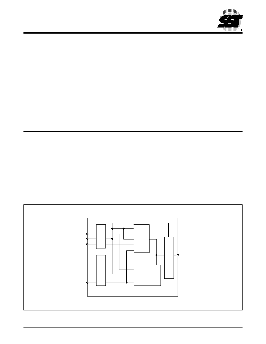
RAMCS#
OE#/RAMCS#
ROMCS#
WE#
AMS-A0
Note: AMS = Most Significant Address
DQ7-DQ0
ROMCS#
RAM
ROM
WE#
OE#
OE#
1134 B1.2
Control
Circuit
Address Buff
er
Data Buff
er
F
UNCTIONAL
B
LOCK
D
IAGRAM
4 Mbit ROM + 1 Mbit / 256 Kbit SRAM
ROM/RAM Combo
SST30VR041 / SST30VR043
SST30VR041 / 0434Mb Mask ROM (x8) + 1Mb / 256Kb SRAM (x8) Combo
2
Data Sheet
4 Mbit ROM + 1 Mbit / 256 Kbit SRAM ROM/RAM Combo
SST30VR041 / SST30VR043
©2003 Silicon Storage Technology, Inc.
S71134-03-000
8/03
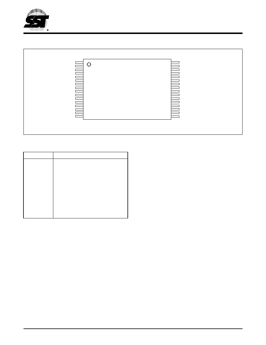
FIGURE 1: P
IN
A
SSIGNMENTS
FOR
32-
LEAD
TSOP
TABLE
1: P
IN
D
ESCRIPTION
Symbol
Pin Name
A
MS
1
-A
0
1. A
MS
= Most significant address
Address Inputs:
ROM: A
MS
= A
18
RAM: A
MS
= A
16
for SST30VR041
A
14
for SST30VR043
WE#
Write Enable Input
OE#/RAMCS#
Output Enable/RAM Enable Input
ROMCS#
ROM Enable Input
DQ
7
-DQ
0
Data Input/Output
V
DD
Power Supply
V
SS
Ground
T1.3 1134
A11
A9
A8
A13
A14
A17
WE#
VDD
A18
A16
A15
A12
A7
A6
A5
A4
1
2
3
4
5
6
7
8
9
10
11
12
13
14
15
16
OE#/RAMCS#
A10
ROMCS#
DQ7
DQ6
DQ5
DQ4
DQ3
VSS
DQ2
DQ1
DQ0
A0
A1
A2
A3
32
31
30
29
28
27
26
25
24
23
22
21
20
19
18
17
1134 32-tsop P1.0
Standard Pinout
Top View
Die Up
Data Sheet
4 Mbit ROM + 1 Mbit / 256 Kbit SRAM ROM/RAM Combo
SST30VR041 / SST30VR043
3
©2003 Silicon Storage Technology, Inc.
S71134-03-000
8/03
Absolute Maximum Stress Ratings (Applied conditions greater than those listed under "Absolute Maximum
Stress Ratings" may cause permanent damage to the device. This is a stress rating only and functional operation
of the device at these conditions or conditions greater than those defined in the operational sections of this data
sheet is not implied. Exposure to absolute maximum stress rating conditions may affect device reliability.)
Operating Temperature . . . . . . . . . . . . . . . . . . . . . . . . . . . . . . . . . . . . . . . . . . . . . . . . . . . . . . . . . . . -20∞C to +85∞C
Storage Temperature . . . . . . . . . . . . . . . . . . . . . . . . . . . . . . . . . . . . . . . . . . . . . . . . . . . . . . . . . . . -65∞C to +150∞C
Voltage on Any Pin Relative to V
SS
. . . . . . . . . . . . . . . . . . . . . . . . . . . . . . . . . . . . . . . . . . . . . . . . -0.5V to V
DD
+0.5V
Voltage on V
DD
Supply Relative to V
SS
. . . . . . . . . . . . . . . . . . . . . . . . . . . . . . . . . . . . . . . . . . . . . . . . . -0.5V to 4.0V
Power Dissipation. . . . . . . . . . . . . . . . . . . . . . . . . . . . . . . . . . . . . . . . . . . . . . . . . . . . . . . . . . . . . . . . . . . . . . . . 1.0W
Soldering Temperature (10 Seconds Lead Only) . . . . . . . . . . . . . . . . . . . . . . . . . . . . . . . . . . . . . . . . . . . . . . 260∞C
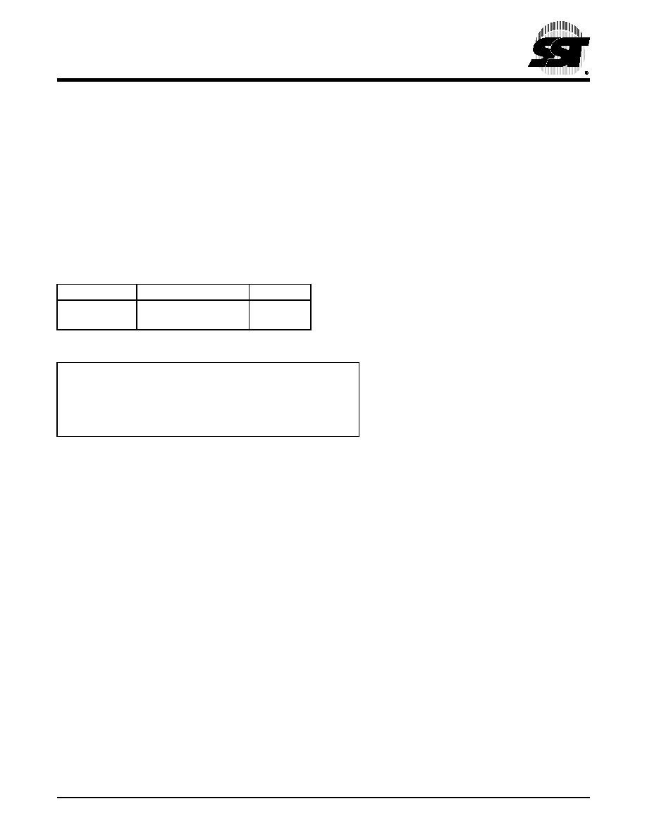
O
PERATING
R
ANGE
Range
Ambient Temp
V
DD
Commercial
0∞C to +70∞C
2.7-3.3V
Extended
-20∞C to +85∞C
2.7-3.3V
AC C
ONDITIONS
OF
T
EST
Input Pulse Level
. . . . . . . . . . . . . . . . . . . . 0-V
DD
Input & Output Timing Reference Levels
. . . V
DD
/2
Input Rise/Fall Time . . . . . . . . . . . . . . . . . . . 5 ns
Output Load . . . . . . . . . . . . . . . . . . . . . . . . . C
L
= 30 pF for 70 ns
Output Load . . . . . . . . . . . . . . . . . . . . . . . . . C
L
= 100 pF for 150 ns
4
Data Sheet
4 Mbit ROM + 1 Mbit / 256 Kbit SRAM ROM/RAM Combo
SST30VR041 / SST30VR043
©2003 Silicon Storage Technology, Inc.
S71134-03-000
8/03
TABLE
2: R
ECOMMENDED
DC O
PERATING
C
ONDITIONS
Symbol
Parameter
Min
Max
Units
V
DD
Supply Voltage
2.7
3.3
V
V
SS
Ground
0
0
V
V
IH
Input High Voltage
2.4
V
DD
+ 0.5
V
V
IL
Input Low Voltage
-0.3
0.3
V
T2.0 1134
TABLE
3: DC O
PERATING
C
HARACTERISTICS
Symbol
Parameter
V
DD
= 2.7-3.3V
Test Conditions
Min
Max
Units
I
DD1
ROM Operating Supply Current
4.0+1.1(f)
1
1. f = Frequency of operation (MHz) = 1/cycle time
mA
ROMCS#=V
IL
, RAMCS#=V
IH
,
V
IN
=V
IH
or V
IL,
I
I/O
=Opens
I
DD2
SRAM Operating Supply Current
2.5+1(f)
1
mA
ROMCS#=V
IH
, RAMCS#=V
IL
, I
I/O
=Opens
I
SB
Standby V
DD
Current
10
µA
ROMCS#
V
DD
-0.2V, RAMCS#
V
DD
-0.2V
V
IN
V
DD
-0.2V or V
IN
0.2V
I
LI
Input Leakage Current
-1
1
µA
V
IN
=V
SS
to V
DD
I
LO
Output Leakage Current
-1
1
µA
ROMCS#=RAMCS#=V
IH
or OE#=V
IH
or
WE#=V
IL
, V
I/O
=V
SS
to V
DD
V
OL
Output Low Voltage
0.4
V
I
OL
=1.0 mA
V
OH
Output High Voltage
2.2
V
I
OH
=-0.5 mA
T3.5 1134
TABLE
4: C
APACITANCE
(Ta = 25∞C, f=1 Mhz)
Parameter
Description
Test Condition
Maximum
C
I/O
1
1. This parameter is measured only for initial qualification and after a design or process change that could affect this parameter.
I/O Pin Capacitance
V
I/O
= 0V
8 pF
C
IN
1
Input Capacitance
V
IN
= 0V
6 pF
T4.1 1134
Data Sheet
4 Mbit ROM + 1 Mbit / 256 Kbit SRAM ROM/RAM Combo
SST30VR041 / SST30VR043
5
©2003 Silicon Storage Technology, Inc.
S71134-03-000
8/03
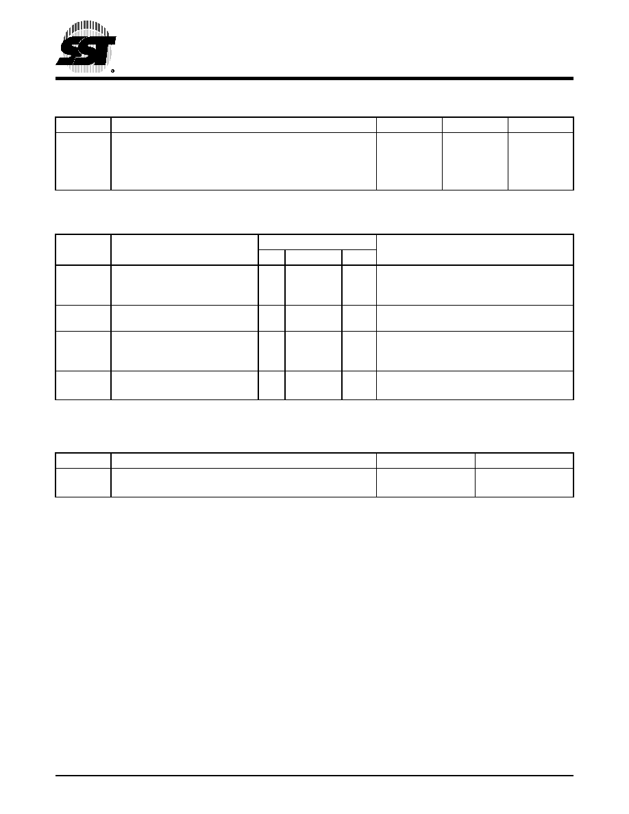
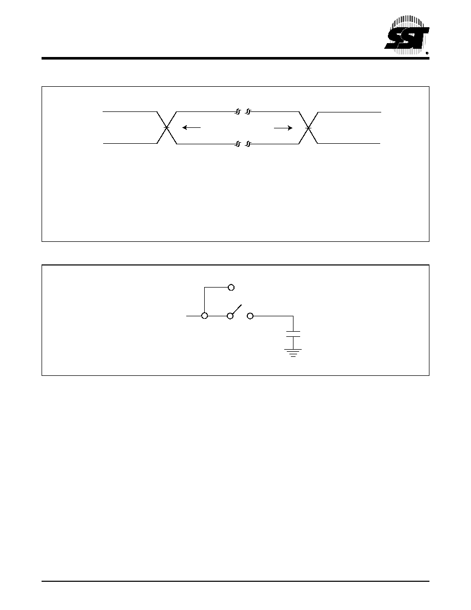
FIGURE 2: AC I
NPUT
/O
UTPUT
R
EFERENCE
W
AVEFORMS
FIGURE 3: A T
EST
L
OAD
E
XAMPLE
1134 F07.0
REFERENCE POINTS
OUTPUT
INPUT
VIT
VIHT
VILT
VOT
AC test inputs are driven at V
IHT
(0.9 V
DD
) for a logic "1" and V
ILT
(0.1 V
DD
) for a logic "0". Measurement reference points
for inputs and outputs are V
IT
(0.5 V
DD
) and V
OT
(0.5 V
DD
). Input rise and fall times (10%
90%) are <5 ns.
Note: V
IT
- V
INPUT
Test
V
OT
- V
OUTPUT
Test
V
IHT
- V
INPUT
HIGH Test
V
ILT
- V
INPUT
LOW Test
1134 F08.0
TO TESTER
TO DUT
CL