©2003 Silicon Storage Technology, Inc.
S71171-08-000
8/03
1
The SST logo and SuperFlash are registered trademarks of Silicon Storage Technology, Inc.
MPF and ComboMemory are trademarks of Silicon Storage Technology, Inc.
These specifications are subject to change without notice.
Data Sheet
FEATURES:
∑
MPF + SRAM ComboMemory
≠ SST32HF162: 1M x16 Flash + 128K x16 SRAM
≠ SST32HF164: 1M x16 Flash + 256K x16 SRAM
∑
Single 2.7-3.3V Read and Write Operations
∑
Concurrent Operation
≠ Read from or write to SRAM while
Erase/Program Flash
∑
Superior Reliability
≠ Endurance: 100,000 Cycles (typical)
≠ Greater than 100 years Data Retention
∑
Low Power Consumption:
≠ Active Current: 15 mA (typical) for
Flash or SRAM Read
≠ Standby Current: 20 µA (typical)
∑
Flexible Erase Capability
≠ Uniform 2 KWord sectors
≠ Uniform 32 KWord size blocks
∑
Fast Read Access Times:
≠ Flash: 70 ns
≠ SRAM: 70 ns
∑
Latched Address and Data for Flash
∑
Flash Fast Erase and Word-Program:
≠ Sector-Erase Time: 18 ms (typical)
≠ Block-Erase Time: 18 ms (typical)
≠ Chip-Erase Time: 70 ms (typical)
≠ Word-Program Time: 14 µs (typical)
≠ Chip Rewrite Time:
SST32HF162/164: 15 seconds (typical)
∑
Flash Automatic Erase and Program Timing
≠ Internal V
PP
Generation
∑
Flash End-of-Write Detection
≠ Toggle Bit
≠ Data# Polling
∑
CMOS I/O Compatibility
∑
JEDEC Standard Command Set
∑
Package Available
≠ 48-ball LBGA (10mm x 12mm)
PRODUCT DESCRIPTION
The SST32HF162/164 ComboMemory devices integrate a
1M x16 CMOS flash memory bank with a 128K x16 or
256K x16 CMOS SRAM memory bank in a Multi-Chip
Package (MCP), manufactured with SST's proprietary, high
performance SuperFlash technology.
Featuring high performance Word-Program, the flash
memory bank provides a maximum Word-Program time of
14 µsec. The entire flash memory bank can be erased and
programmed word-by-word in 15 seconds (typically) for the
SST32HF162/164, when using interface features such as
Toggle Bit or Data# Polling to indicate the completion of
Program operation. To protect against inadvertent flash
write, the SST32HF162/164 devices contain on-chip hard-
ware and software data protection schemes. The
SST32HF162/164 devices offer a guaranteed endurance
of 10,000 cycles. Data retention is rated at greater than 100
years.
The SST32HF162/164 devices consist of two independent
memory banks with respective bank enable signals. The
Flash and SRAM memory banks are superimposed in the
same memory address space. Both memory banks share
common address lines, data lines, WE# and OE#. The
memory bank selection is done by memory bank enable
signals. The SRAM bank enable signal, BES# selects the
SRAM bank. The flash memory bank enable signal, BEF#
selects the flash memory bank. The WE# signal has to be
used with Software Data Protection (SDP) command
sequence when controlling the Erase and Program opera-
tions in the flash memory bank. The SDP command
sequence protects the data stored in the flash memory
bank from accidental alteration.
The SST32HF162/164 provide the added functionality of
being able to simultaneously read from or write to the
SRAM bank while erasing or programming in the flash
memory bank. The SRAM memory bank can be read or
written while the flash memory bank performs Sector-
Erase, Bank-Erase, or Word-Program concurrently. All
flash memory Erase and Program operations will automati-
cally latch the input address and data signals and complete
the operation in background without further input stimulus
requirement. Once the internally controlled Erase or Pro-
gram cycle in the flash bank has commenced, the SRAM
bank can be accessed for Read or Write.
The SST32HF162/164 devices are suited for applications
that use both flash memory and SRAM memory to store
code or data. For systems requiring low power and small
form factor, the SST32HF162/164 devices significantly
improve performance and reliability, while lowering power
consumption, when compared with multiple chip solutions.
The SST32HF162/164 inherently use less energy during
erase and program than alternative flash technologies. The
total energy consumed is a function of the applied voltage,
Multi-Purpose Flash (MPF) + SRAM ComboMemory
SST32HF162 / SST32HF164
SST32HF162 / 16416Mb Flash + 2Mb SRAM, 16Mb Flash + 4Mb SRAM
(x16) MCP ComboMemories
2
Data Sheet
Multi-Purpose Flash (MPF) + SRAM ComboMemory
SST32HF162 / SST32HF164
©2003 Silicon Storage Technology, Inc.
S71171-08-000
8/03
current, and time of application. Since for any given voltage
range, the SuperFlash technology uses less current to pro-
gram and has a shorter erase time, the total energy con-
sumed during any Erase or Program operation is less than
alternative flash technologies.
SuperFlash technology provides fixed Erase and Pro-
gram times, independent of the number of Erase/Pro-
gram cycles that have occurred. Therefore the system
software or hardware does not have to be modified or de-
rated as is necessary with alternative flash technologies,
whose Erase and Program times increase with accumu-
lated Erase/Program cycles.
Device Operation
The ComboMemory uses BES# and BEF# to control oper-
ation of either the SRAM or the flash memory bank. When
BES# is low, the SRAM Bank is activated for Read and
Write operation. When BEF# is low the flash bank is acti-
vated for Read, Program or Erase operation. BES# and
BEF# cannot be at low level at the same time. If BES# and
BEF# are both asserted to low level bus contention will
result and the device may suffer permanent damage.
All address, data, and control lines are shared by SRAM
Bank and flash bank which minimizes power consumption
and loading. The device goes into standby when both bank
enables are high.
SRAM Operation
With BES# low and BEF# high, the SST32HF162 operate
as 128K x16 CMOS SRAM, and the SST32HF164 oper-
ates as 256K x16 CMOS SRAM, with fully static operation
requiring no external clocks or timing strobes. The
SST32HF162 SRAM is mapped into the first 128 KWord
address space of the device, and the SST32HF164 SRAM
is mapped into the first 256 KWord address space. When
BES# and BEF# are high, both memory banks are dese-
lected and the device enters standby mode. Read and
Write cycle times are equal. The control signals UBS# and
LBS# provide access to the upper data byte and lower data
byte. See Table 3 for SRAM read and write data byte con-
trol modes of operation.
SRAM Read
The SRAM Read operation of the SST32HF162/164 is
controlled by OE# and BES#, both have to be low with
WE# high for the system to obtain data from the outputs.
BES# is used for SRAM bank selection. OE# is the output
control and is used to gate data from the output pins. The
data bus is in high impedance state when OE# is high. See
Figure 2 for the Read cycle timing diagram.
SRAM Write
The SRAM Write operation of the SST32HF162/164 is
controlled by WE# and BES# being low for the system to
write to the SRAM. During the Word-Write operation, the
addresses and data are referenced to the rising edge of
WE# or BES#, which ever occurs first. The write time is
measured from the last falling edge to the rising edge of
WE# or BES#. Refer to the Write cycle timing diagrams,
Figures 3 and 4, for further details.
Flash Operation
With BEF# active, the SST32HF162/164 operate as 1M
x16 flash memory. The flash memory bank is read using
the common address lines, data lines, WE# and OE#.
Erase and Program operations are initiated with the
JEDEC standard SDP command sequences. Address and
data are latched during the SDP commands and during the
internally timed Erase and Program operations.
Flash Read
The Read operation of the SST32HF162/164 devices is
controlled by BEF# and OE#. Both have to be low, with
WE# high, for the system to obtain data from the outputs.
BEF# is used for flash memory bank selection. When
BEF# and BES# are high, both banks are deselected and
only standby power is consumed. OE# is the output con-
trol and is used to gate data from the output pins. The data
bus is in high impedance state when OE# is high. Refer to
Figure 5 for further details.
Flash Erase/Program Operation
SDP commands are used to initiate the flash memory bank
Program and Erase operations of the SST32HF162/164.
SDP commands are loaded to the flash memory bank
using standard microprocessor write sequences. A com-
mand is loaded by asserting WE# low while keeping BEF#
low and OE# high. The address is latched on the falling
edge of WE# or BEF#, whichever occurs last. The data is
latched on the rising edge of WE# or BEF#, whichever
occurs first.
Flash Word-Program Operation
The flash memory bank of the SST32HF162/164 devices
is programmed on a word-by-word basis. Before Program
operations, the memory must be erased first. The Program
operation consists of three steps. The first step is the three-
byte load sequence for Software Data Protection. The sec-
ond step is to load word address and word data. During the
Word-Program operation, the addresses are latched on the
falling edge of either BEF# or WE#, whichever occurs last.
Data Sheet
Multi-Purpose Flash (MPF) + SRAM ComboMemory
SST32HF162 / SST32HF164
3
©2003 Silicon Storage Technology, Inc.
S71171-08-000
8/03
The data is latched on the rising edge of either BEF# or
WE#, whichever occurs first. The third step is the internal
Program operation which is initiated after the rising edge of
the fourth WE# or BEF#, whichever occurs first. The Pro-
gram operation, once initiated, will be completed, within 20
µs. See Figures 6 and 7 for WE# and BEF# controlled Pro-
gram operation timing diagrams and Figure 17 for flow-
charts. During the Program operation, the only valid flash
Read operations are Data# Polling and Toggle Bit. During
the internal Program operation, the host is free to perform
additional tasks. Any SDP commands loaded during the
internal Program operation will be ignored.
Flash Sector/Block-Erase Operation
The Flash Sector/Block-Erase operation allows the system
to erase the device on a sector-by-sector (or block-by-
block) basis. The SST32HF162/164 offer both Sector-
Erase and Block-Erase mode. The sector architecture is
based on uniform sector size of 2 KWord. The Block-Erase
mode is based on uniform block size of 32 KWord. The
Sector-Erase operation is initiated by executing a six-byte
command sequence with Sector-Erase command (30H)
and sector address (SA) in the last bus cycle. The address
lines A
19
-A
11
, for SST32HF162/164, are used to determine
the sector address. The Block-Erase operation is initiated
by executing a six-byte command sequence with Block-
Erase command (50H) and block address (BA) in the last
bus cycle. The address lines A
19
-A
15
, for SST32HF162/
164, are used to determine the block address. The sector
or block address is latched on the falling edge of the sixth
WE# pulse, while the command (30H or 50H) is latched on
the rising edge of the sixth WE# pulse. The internal Erase
operation begins after the sixth WE# pulse. The End-of-
Erase operation can be determined using either Data#
Polling or Toggle Bit methods. See Figures 11 and 12 for
timing waveforms. Any commands issued during the Sec-
tor- or Block-Erase operation are ignored.
Flash Chip-Erase Operation
The SST32HF162/164 provide a Chip-Erase operation,
which allows the user to erase the entire memory array to
the "1" state. This is useful when the entire device must be
quickly erased.
The Chip-Erase operation is initiated by executing a six-
byte command sequence with Chip-Erase command (10H)
at address 5555H in the last byte sequence. The Erase
operation begins with the rising edge of the sixth WE# or
CE#, whichever occurs first. During the Erase operation,
the only valid read is Toggle Bit or Data# Polling. See Table
4 for the command sequence, Figure 9 for timing diagram,
and Figure 20 for the flowchart. Any commands issued dur-
ing the Chip-Erase operation are ignored.
Write Operation Status Detection
The SST32HF162/164 provide two software means to
detect the completion of a write (Program or Erase) cycle,
in order to optimize the system Write cycle time. The soft-
ware detection includes two status bits: Data# Polling
(DQ
7
) and Toggle Bit (DQ
6
). The End-of-Write detection
mode is enabled after the rising edge of WE#, which ini-
tiates the internal Program or Erase operation.
The actual completion of the nonvolatile write is asynchro-
nous with the system; therefore, either a Data# Polling or
Toggle Bit read may be simultaneous with the completion
of the Write cycle. If this occurs, the system may possibly
get an erroneous result, i.e., valid data may appear to con-
flict with either DQ
7
or DQ
6.
In order to prevent spurious
rejection, if an erroneous result occurs, the software routine
should include a loop to read the accessed location an
additional two (2) times. If both reads are valid, then the
device has completed the Write cycle, otherwise the rejec-
tion is valid.
Flash Data# Polling (DQ
7
)
When the SST32HF162/164 flash memory banks are in
the internal Program operation, any attempt to read DQ
7
will produce the complement of the true data. Once the
Program operation is completed, DQ
7
will produce true
data. Note that even though DQ
7
may have valid data
immediately following the completion of an internal Write
operation, the remaining data outputs may still be invalid:
valid data on the entire data bus will appear in subsequent
successive Read cycles after an interval of 1 µs. During
internal Erase operation, any attempt to read DQ
7
will pro-
duce a `0'. Once the internal Erase operation is completed,
DQ
7
will produce a `1'. The Data# Polling is valid after the
rising edge of the fourth WE# (or BEF#) pulse for Program
operation. For Sector- or Block-Erase, the Data# Polling is
valid after the rising edge of the sixth WE# (or BEF#) pulse.
See Figure 8 for Data# Polling timing diagram and Figure
18 for a flowchart.
Flash Toggle Bit (DQ
6
)
During the internal Program or Erase operation, any con-
secutive attempts to read DQ
6
will produce alternating 1s
and 0s, i.e., toggling between 1 and 0. When the internal
Program or Erase operation is completed, the toggling will
stop. The flash memory bank is then ready for the next
operation. The Toggle Bit is valid after the rising edge of the
fourth WE# (or BEF#) pulse for Program operation. For
Sector- or Bank-Erase, the Toggle Bit is valid after the rising
edge of the sixth WE# (or BEF#) pulse. See Figure 9 for
Toggle Bit timing diagram and Figure 18 for a flowchart.
4
Data Sheet
Multi-Purpose Flash (MPF) + SRAM ComboMemory
SST32HF162 / SST32HF164
©2003 Silicon Storage Technology, Inc.
S71171-08-000
8/03
Flash Memory Data Protection
The SST32HF162/164 flash memory bank provides both
hardware and software features to protect nonvolatile data
from inadvertent writes.
Flash Hardware Data Protection
Noise/Glitch Protection: A WE# or BEF# pulse of less than
5 ns will not initiate a Write cycle.
V
DD
Power Up/Down Detection: The Write operation is
inhibited when V
DD
is less than 1.5V.
Write Inhibit Mode: Forcing OE# low, BEF# high, or WE#
high will inhibit the flash Write operation. This prevents
inadvertent writes during power-up or power-down.
Flash Software Data Protection (SDP)
The SST32HF162/164 provide the JEDEC approved soft-
ware data protection scheme for all flash memory bank
data alteration operations, i.e., Program and Erase. Any
Program operation requires the inclusion of a series of
three-byte sequence. The three byte-load sequence is
used to initiate the Program operation, providing optimal
protection from inadvertent Write operations, e.g., during
the system power-up or power-down. Any Erase operation
requires the inclusion of six-byte load sequence. The
SST32HF162/164 devices are shipped with the software
data protection permanently enabled. See Table 4 for the
specific software command codes. During SDP command
sequence, invalid SDP commands will abort the device to
the read mode, within Read Cycle Time (T
RC
).
Concurrent Read and Write Operations
The SST32HF162/164 provide the unique benefit of being
able to read from or write to SRAM, while simultaneously
erasing or programming the flash. This allows data alter-
ation code to be executed from SRAM, while altering the
data in flash. The following table lists all valid states.
The device will ignore all SDP commands when an Erase
or Program operation is in progress. Note that Product
Identification commands use SDP; therefore, these com-
mands will also be ignored while an Erase or Program
operation is in progress.
Product Identification
The Product Identification mode identifies the devices as
the SST32HFxxx and manufacturer as SST. This mode
may be accessed by software operations only. The
hardware device ID Read operation, which is typically
used by programmers, cannot be used on this device
because of the shared lines between flash and SRAM
in the multi-chip package. Therefore, application of
high voltage to pin A
9
may damage this device. Users
may use the software Product Identification operation to
identify the part (i.e., using the device ID) when using multi-
ple manufacturers in the same socket. For details, see
Tables 3 and 4 for software operation, Figure 13 for the
software ID entry and read timing diagram and Figure 19
for the ID entry command sequence flowchart.
Product Identification Mode Exit/Reset
In order to return to the standard read mode, the Software
Product Identification mode must be exited. Exiting is
accomplished by issuing the Exit ID command sequence,
which returns the device to the Read operation. Please
note that the software reset command is ignored during an
internal Program or Erase operation. See Table 4 for soft-
ware command codes, Figure 14 for timing waveform and
Figure 19 for a flowchart.
Design Considerations
SST recommends a high frequency 0.1 µF ceramic capac-
itor to be placed as close as possible between V
DD
and
V
SS
, e.g., less than 1 cm away from the V
DD
pin of the
device. Additionally, a low frequency 4.7 µF electrolytic
capacitor from V
DD
to V
SS
should be placed within 1 cm of
the V
DD
pin.
C
ONCURRENT
R
EAD
/W
RITE
S
TATE
T
ABLE
Flash
SRAM
Program/Erase
Read
Program/Erase
Write
TABLE
1: P
RODUCT
I
DENTIFICATION
Address
Data
Manufacturer's ID
0000H
00BFH
Device ID
SST32HF162/164
0001H
2782H
T1.2 1171
Data Sheet
Multi-Purpose Flash (MPF) + SRAM ComboMemory
SST32HF162 / SST32HF164
5
©2003 Silicon Storage Technology, Inc.
S71171-08-000
8/03
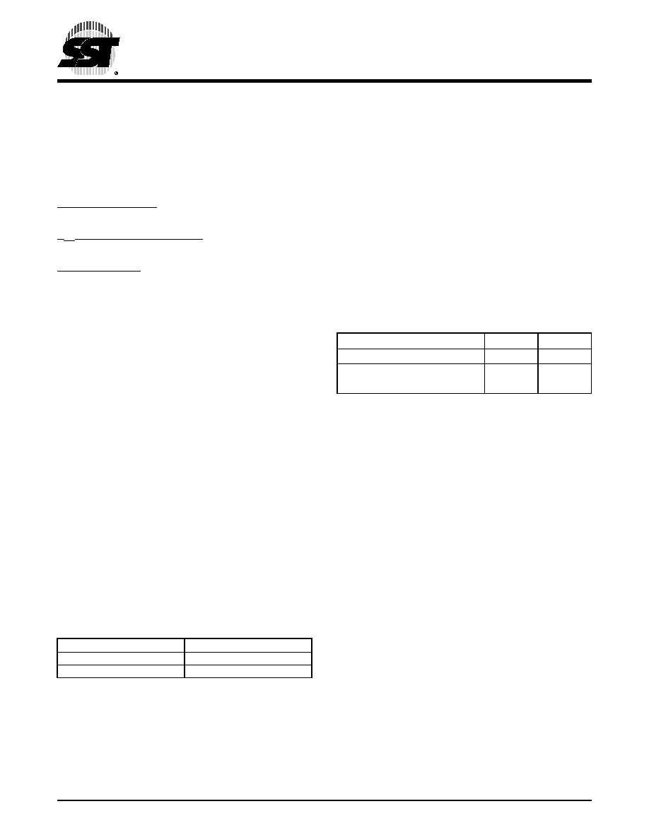
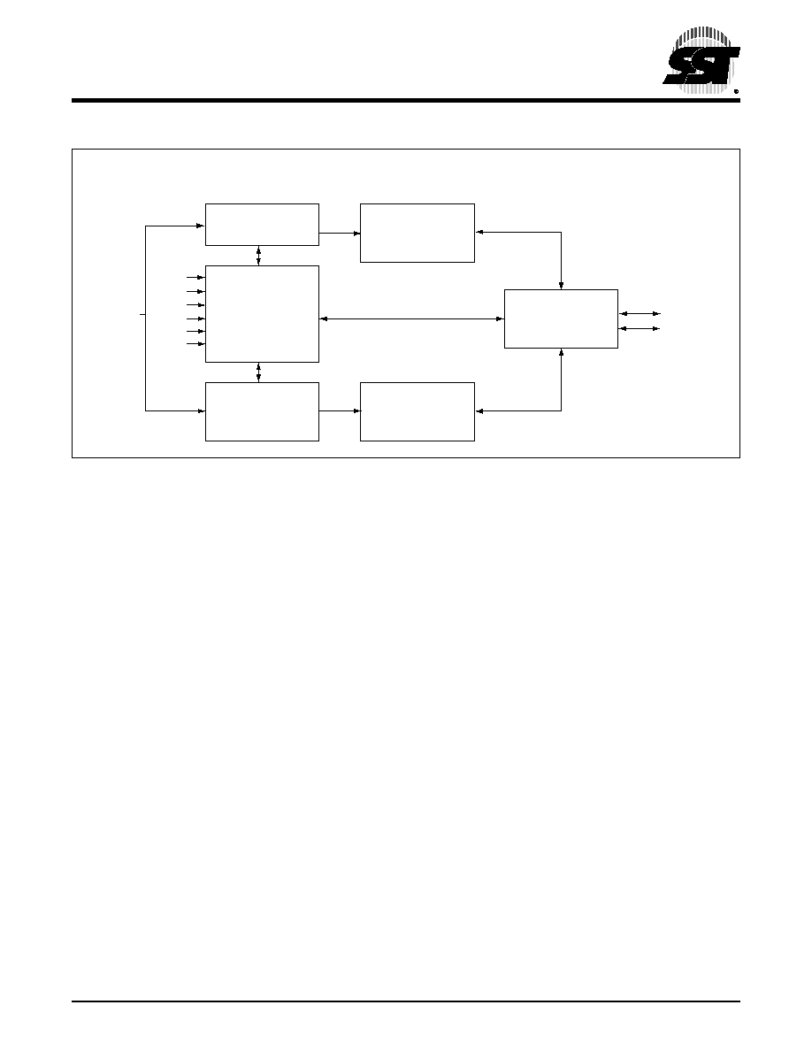
I/O Buffers
1171 B1.1
Address Buffers
DQ15 - DQ8
AMS
(1)
-A0
WE#
SuperFlash
Memory
SRAM
Control Logic
BES#
BEF#
OE#
Address Buffers
& Latches
LBS#
UBS#
DQ7 - DQ0
F
UNCTIONAL
B
LOCK
D
IAGRAM