
©2004 Silicon Storage Technology, Inc.
S71256-00-000
3/04
1
The SST logo and SuperFlash are registered trademarks of Silicon Storage Technology, Inc. Intel is a registered trademark of Intel Corporation.
CSF and ComboMemory are trademarks of Silicon Storage Technology, Inc.
These specifications are subject to change without notice.
Advance Information
FEATURES:
∑
Flash Organization: 1M x16 or 2M x8
∑
Dual-Bank Architecture for Concurrent
Read/Write Operation
≠ 16 Mbit: 4 Mbit + 12 Mbit
∑
(P)SRAM Organization:
≠ 2 Mbit: 128K x16 or 256K x8
≠ 4 Mbit: 256K x16 or 512K x8
≠ 8 Mbit: 512K x16 or 1024K x8
∑
Single 2.7-3.3V Read and Write Operations
∑
Superior Reliability
≠ Endurance: 100,000 Cycles (typical)
≠ Greater than 100 years Data Retention
∑
Low Power Consumption:
≠ Active Current: 25 mA (typical)
≠ Standby Current: 20 µA (typical)
∑
Hardware Sector Protection (WP#)
≠ Protects 4 outer most sectors (4 KWord) in the
larger bank by holding WP# low and unprotects
by holding WP# high
∑
Hardware Reset Pin (RST#)
≠ Resets the internal state machine to reading
data array
∑
Byte Selection for Flash (CIOF pin)
≠ Selects 8-bit or 16-bit mode
∑
Sector-Erase Capability
≠ Uniform 2 KWord sectors
∑
Block-Erase Capability
≠ Uniform 32 KWord blocks
∑
Read Access Time
≠ Flash: 70 ns
≠ (P)SRAM: 70 ns
∑
Erase-Suspend / Erase-Resume Capabilities
∑
Security ID Feature
≠ SST: 128 bits
≠ User: 128 bits
∑
Latched Address and Data
∑
Fast Erase and Word-/Byte-Program (typical):
≠ Sector-Erase Time: 18 ms
≠ Block-Erase Time: 18 ms
≠ Chip-Erase Time: 35 ms
≠ Word-Program Time: 7 µs
∑
Automatic Write Timing
≠ Internal
V
PP
Generation
∑
End-of-Write Detection
≠ Toggle Bit
≠ Data# Polling
≠ Ready/Busy# pin
∑
CMOS I/O Compatibility
∑
JEDEC Standard Command Set
∑
Packages Available
≠ 56-ball LFBGA (8mm x 10mm)
≠ 62-ball LFBGA (8mm x 10mm)
PRODUCT DESCRIPTION
The SST34HF16x2C/D/S ComboMemory devices inte-
grate either a 1M x16 or 2M x8 CMOS flash memory bank
with either a 128K x16/256K x8, 256K x16/512 x8, or 512K
x16/1024K x8 CMOS SRAM or pseudo SRAM (PSRAM)
memory bank in a multi-chip package (MCP). These
devices are fabricated using SST's proprietary, high-perfor-
mance CMOS SuperFlash technology incorporating the
split-gate cell design and thick-oxide tunneling injector to
attain better reliability and manufacturability compared with
alternate approaches. The SST34HF16x2C/D/S devices
are ideal for applications such as cellular phones, GPS
devices, PDAs, and other portable electronic devices in a
low power and small form factor system.
The SST34HF16x2C/D/S feature dual flash memory bank
architecture allowing for concurrent operations between the
two flash memory banks and the (P)SRAM. The devices
can read data from either bank while an Erase or Program
operation is in progress in the opposite bank. The two flash
memory banks are partitioned into 4 Mbit and 12 Mbit with
top sector protection options for storing boot code, program
code, configuration/parameter data and user data.
The SuperFlash technology provides fixed Erase and Pro-
gram times, independent of the number of Erase/Program
cycles that have occurred. Therefore, the system software
or hardware does not have to be modified or de-rated as is
necessary with alternative flash technologies, whose Erase
and Program times increase with accumulated Erase/Pro-
gram cycles. The SST34HF16x2C/D/S devices offer a
guaranteed endurance of 10,000 cycles. Data retention is
rated at greater than 100 years. With high performance
Word-Program, the flash memory banks provide a typical
Word-Program time of 7 µsec. The entire flash memory
bank can be erased and programmed word-by-word in typ-
ically 4 seconds for the SST34HF16x2C/D/S, when using
interface features such as Toggle Bit, Data# Polling, or RY/
BY# to indicate the completion of Program operation. To
16 Mbit Concurrent SuperFlash + 2/4/8 Mbit SRAM ComboMemory
SST34HF1602C / SST34HF1622C / SST34HF1642C
SST34HF1642D / SST34HF1682D / SST34HF1622S / SST34HF1642S
SST34HF16x2x16Mb CSF + 2/4/8 Mb SRAM (x16) MCP ComboMemory
2
Advance Information
16 Mbit Concurrent SuperFlash + 2/4/8 Mbit SRAM ComboMemory
SST34HF1602C / SST34HF1622C / SST34HF1642C
SST34HF1642D / SST34HF1682D / SST34HF1622S / SST34HF1642S
©2004 Silicon Storage Technology, Inc.
S71256-00-000
3/04
protect against inadvertent flash write, the
SST34HF16x2C/D/S devices contain on-chip hardware
and software data protection schemes.
The flash and (P)SRAM operate as two independent mem-
ory banks with respective bank enable signals. The mem-
ory bank selection is done by two bank enable signals. The
(P)SRAM bank enable signals, BES1# and BES2, select
the (P)SRAM bank (BES1# and BES2 are NC for
SST34HF1602C). The flash memory bank enable signal,
BEF#, has to be used with Software Data Protection (SDP)
command sequence when controlling the Erase and Pro-
gram operations in the flash memory bank. The memory
banks are superimposed in the same memory address
space where they share common address lines, data lines,
WE# and OE# which minimize power consumption and
area.
Designed, manufactured, and tested for applications requir-
ing low power and small form factor, the SST34HF16x2C/
D/S are offered in both commercial and extended tempera-
tures and a small footprint package to meet board space
constraint requirements. See Figures 3 and 4 for pin
assignments.
Device Operation
The SST34HF16x2C/D/S uses BES1#, BES2 and BEF#
to control operation of either the flash or the (P)SRAM
memory bank. When BEF# is low, the flash bank is acti-
vated for Read, Program or Erase operation. When BES1#
is low, and BES2 is high the (P)SRAM is activated for Read
and Write operation. BEF# and BES1# cannot be at low
level, and BES2 cannot be at high level at the same time. If
all bank enable signals are asserted, bus contention
will result and the device may suffer permanent dam-
age. All address, data, and control lines are shared by flash
and (P)SRAM memory banks which minimizes power con-
sumption and loading. The device goes into standby when
BEF# and BES1# bank enables are raised to V
IHC
(Logic
High) or when BEF# is high and BES2 is low.
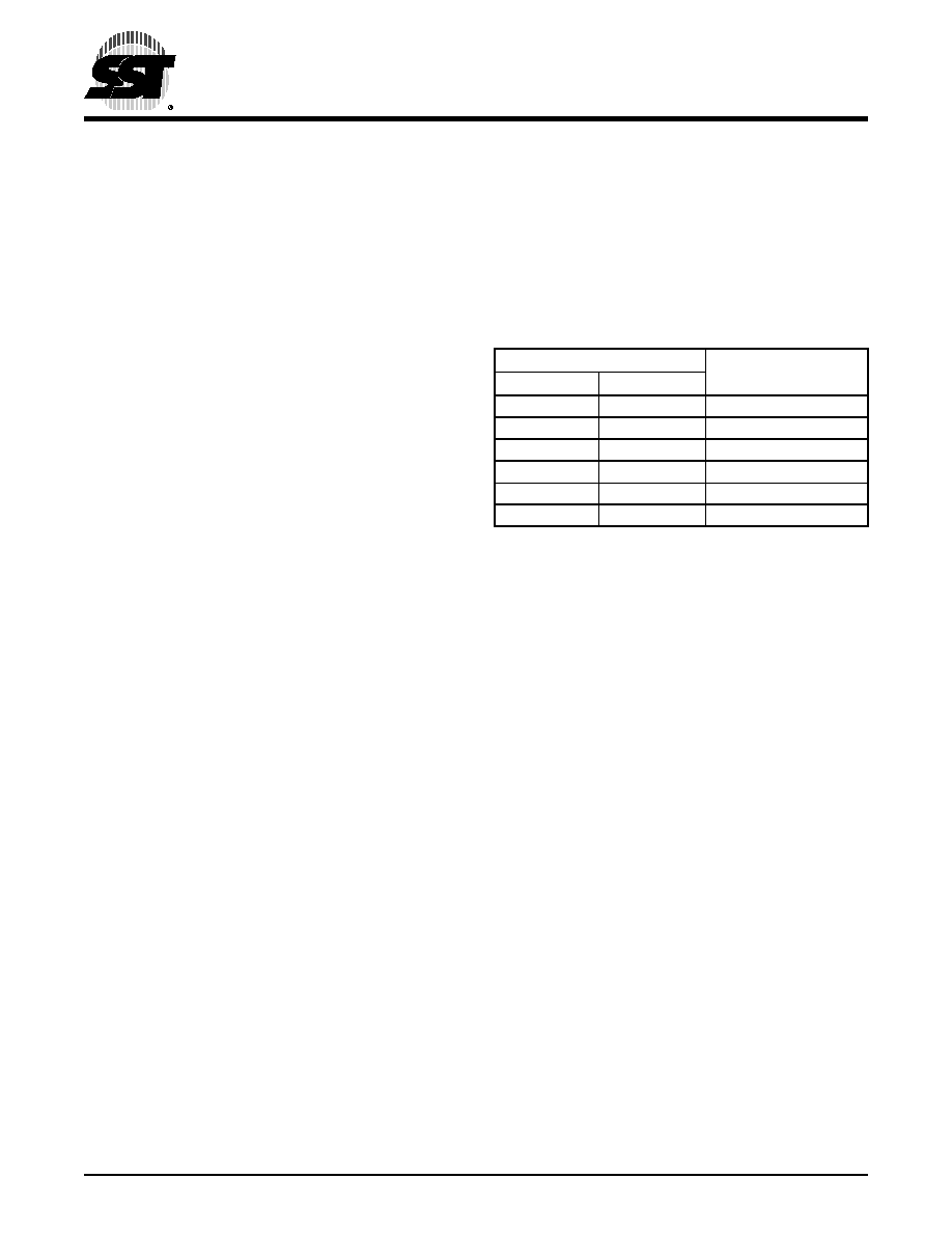
Concurrent Read/Write Operation
Dual bank architecture of SST34HF16x2C/D/S devices
allows the Concurrent Read/Write operation whereby the
user can read from one bank while programming or eras-
ing in the other bank. This operation can be used when the
user needs to read system code in one bank while updat-
ing data in the other bank. See Figures 1 and 2 for dual-
bank memory organization.
Note: For the purposes of this table, write means to Block-, Sector,
or Chip-Erase, or Word-/Byte-Program as applicable to the
appropriate bank.
Flash Read Operation
The Read operation of the SST34HF16x2C/D/S is con-
trolled by BEF# and OE#, both have to be low for the sys-
tem to obtain data from the outputs. BEF# is used for
device selection. When BEF# is high, the chip is dese-
lected and only standby power is consumed. OE# is the
output control and is used to gate data from the output pins.
The data bus is in high impedance state when either BEF#
or OE# is high. Refer to the Read cycle timing diagram for
further details (Figure 8).
C
ONCURRENT
R
EAD
/W
RITE
S
TATES
Flash
(P)SRAM
Bank 1
Bank 2
Read
Write
No Operation
Write
Read
No Operation
Write
No Operation
Read
No Operation
Write
Read
Write
No Operation
Write
No Operation
Write
Write
Advance Information
16 Mbit Concurrent SuperFlash + 2/4/8 Mbit SRAM ComboMemory
SST34HF1602C / SST34HF1622C / SST34HF1642C
SST34HF1642D / SST34HF1682D / SST34HF1622S / SST34HF1642S
3
©2004 Silicon Storage Technology, Inc.
S71256-00-000
3/04
Flash Word-/Byte-Program Operation
These devices are programmed on a word-by-word or
byte-by-byte basis depending on the state of the CIOF pin.
Before programming, one must ensure that the sector
which is being programmed is fully erased.
The Program operation is accomplished in three steps:
1. Software Data Protection is initiated using the
three-byte load sequence.
2. Word address and word data are loaded.
During the Word-Program operation, the
addresses are latched on the falling edge of either
BEF# or WE#, whichever occurs last. The data is
latched on the rising edge of either BEF# or WE#,
whichever occurs first.
3. The internal Program operation is initiated after
the rising edge of the fourth WE# or BEF#, which-
ever occurs first. The Program operation, once ini-
tiated, will be completed typically within 7 µs.
See Figures 9 and 10 for WE# and BEF# controlled Pro-
gram operation timing diagrams and Figure 22 for flow-
charts. During the Program operation, the only valid reads
are Data# Polling and Toggle Bit. During the internal Pro-
gram operation, the host is free to perform additional tasks.
Any commands issued during an internal Program opera-
tion are ignored.
Flash Sector- (Block-) Erase Operation
These devices offer both Sector-Erase and Block-Erase
operations. These operations allow the system to erase the
devices on a sector-by-sector (or block-by-block) basis.
The sector architecture is based on a uniform sector size of
2 KWord. The Block-Erase mode is based on a uniform
block size of 32 KWord. The Sector-Erase operation is initi-
ated by executing a six-byte command sequence with a
Sector-Erase command (30H) and sector address (SA) in
the last bus cycle. The Block-Erase operation is initiated by
executing a six-byte command sequence with Block-Erase
command (50H) and block address (BA) in the last bus
cycle. The sector or block address is latched on the falling
edge of the sixth WE# pulse, while the command (30H or
50H) is latched on the rising edge of the sixth WE# pulse.
The internal Erase operation begins after the sixth WE#
pulse. Any commands issued during the Block- or Sector-
Erase operation are ignored except Erase-Suspend and
Erase-Resume. See Figures 14 and 15 for timing wave-
forms.
Flash Chip-Erase Operation
The SST34HF16x2C/D/S provide a Chip-Erase operation,
which allows the user to erase all sectors/blocks to the "1"
state. This is useful when the device must be quickly
erased.
The Chip-Erase operation is initiated by executing a six-
byte command sequence with Chip-Erase command (10H)
at address 5555H in the last byte sequence. The Erase
operation begins with the rising edge of the sixth WE# or
BEF#, whichever occurs first. During the Erase operation,
the only valid read is Toggle Bits or Data# Polling. See
Table 7 for the command sequence, Figure 13 for timing
diagram, and Figure 26 for the flowchart. Any commands
issued during the Chip-Erase operation are ignored. When
WP# is low, any attempt to Chip-Erase will be ignored.
Flash Erase-Suspend/-Resume Operations
The Erase-Suspend operation temporarily suspends a
Sector- or Block-Erase operation thus allowing data to be
read from any memory location, or program data into any
sector/block that is not suspended for an Erase operation.
The operation is executed by issuing a one-byte command
sequence with Erase-Suspend command (B0H). The
device automatically enters read mode within 20 µs after
the Erase-Suspend command had been issued. Valid data
can be read from any sector or block that is not suspended
from an Erase operation. Reading at address location
within erase-suspended sectors/blocks will output DQ
2
tog-
gling and DQ
6
at "1". While in Erase-Suspend mode, a
Word-/Byte-Program operation is allowed except for the
sector or block selected for Erase-Suspend. To resume
Sector-Erase or Block-Erase operation which has been
suspended, the system must issue an Erase-Resume
command. The operation is executed by issuing a one-byte
command sequence with Erase Resume command (30H)
at any address in the one-byte sequence.

4
Advance Information
16 Mbit Concurrent SuperFlash + 2/4/8 Mbit SRAM ComboMemory
SST34HF1602C / SST34HF1622C / SST34HF1642C
SST34HF1642D / SST34HF1682D / SST34HF1622S / SST34HF1642S
©2004 Silicon Storage Technology, Inc.
S71256-00-000
3/04
Flash Write Operation Status Detection
The SST34HF16x2C/D/S provide one hardware and two
software means to detect the completion of a Write (Pro-
gram or Erase) cycle, in order to optimize the system
Write cycle time. The hardware detection uses the
Ready/Busy# (RY/BY#) pin. The software detection
includes two status bits: Data# Polling (DQ
7
) and Toggle
Bit (DQ
6
). The End-of-Write detection mode is enabled
after the rising edge of WE#, which initiates the internal
Program or Erase operation.
The actual completion of the nonvolatile write is asynchro-
nous with the system; therefore, either a Ready/Busy# (RY/
BY#), Data# Polling (DQ
7
) or Toggle Bit (DQ
6
) read may be
simultaneous with the completion of the Write cycle. If this
occurs, the system may possibly get an erroneous result,
i.e., valid data may appear to conflict with either DQ
7
or
DQ
6
. In order to prevent spurious rejection, if an erroneous
result occurs, the software routine should include a loop to
read the accessed location an additional two (2) times. If
both reads are valid, then the device has completed the
Write cycle, otherwise the rejection is valid.
Ready/Busy# (RY/BY#)
The SST34HF16x2C/D/S include a Ready/Busy# (RY/
BY#) output signal. RY/BY# is an open drain output pin that
indicates whether an Erase or Program operation is in
progress. Since RY/BY# is an open drain output, it allows
several devices to be tied in parallel to V
DD
via an external
pull-up resistor. After the rising edge of the final WE# pulse
in the command sequence, the RY/BY# status is valid.
When RY/BY# is actively pulled low, it indicates that an
Erase or Program operation is in progress. When RY/BY#
is high (Ready), the devices may be read or left in standby
mode.
Byte/Word (CIOF)
The device includes a CIOF pin to control whether the
device data I/O pins operate x8 or x16. If the CIOF pin is at
logic "1" (V
IH
) the device is in x16 data configuration: all
data I/0 pins DQ
0
-DQ
15
are active and controlled by BEF#
and OE#.
If the CIOF pin is at logic "0", the device is in x8 data config-
uration: only data I/O pins DQ
0
-DQ
7
are active and con-
trolled by BEF# and OE#. The remaining data pins DQ
8
-
DQ
14
are at Hi-Z, while pin DQ
15
is used as the address
input A
-1
for the Least Significant Bit of the address bus.
Flash Data# Polling (DQ
7
)
When the devices are in an internal Program operation, any
attempt to read DQ
7
will produce the complement of the
true data. Once the Program operation is completed, DQ
7
will produce true data. During internal Erase operation, any
attempt to read DQ
7
will produce a `0'. Once the internal
Erase operation is completed, DQ
7
will produce a `1'. The
Data# Polling is valid after the rising edge of fourth WE# (or
BEF#) pulse for Program operation. For Sector-, Block-, or
Chip-Erase, the Data# Polling is valid after the rising edge
of sixth WE# (or BEF#) pulse. See Figure 11 for Data# Poll-
ing (DQ
7
) timing diagram and Figure 23 for a flowchart.
Toggle Bits (DQ
6
and DQ
2
)
During the internal Program or Erase operation, any con-
secutive attempts to read DQ
6
will produce alternating "1"s
and "0"s, i.e., toggling between 1 and 0. When the internal
Program or Erase operation is completed, the DQ
6
bit will
stop toggling. The device is then ready for the next opera-
tion. The toggle bit is valid after the rising edge of the fourth
WE# (or BEF#) pulse for Program operations. For Sector-,
Block-, or Chip-Erase, the toggle bit (DQ
6
) is valid after the
rising edge of sixth WE# (or BEF#) pulse. DQ
6
will be set to
"1" if a Read operation is attempted on an Erase-sus-
pended Sector/Block. If Program operation is initiated in a
sector/block not selected in Erase-Suspend mode, DQ
6
will
toggle.
An additional Toggle Bit is available on DQ
2
, which can be
used in conjunction with DQ
6
to check whether a particular
sector is being actively erased or erase-suspended. Table 1
shows detailed status bit information. The Toggle Bit (DQ
2
)
is valid after the rising edge of the last WE# (or BEF#)
pulse of a Write operation. See Figure 12 for Toggle Bit tim-
ing diagram and Figure 23 for a flowchart.
Note: DQ
7,
DQ
6,
and DQ
2
require a valid address when reading
status information.
TABLE
1: W
RITE
O
PERATION
S
TATUS
Status
DQ
7
DQ
6
DQ
2
RY/BY#
Normal
Operation
Standard
Program
DQ7#
Toggle
No Toggle
0
Standard
Erase
0
Toggle
Toggle
0
Erase-
Suspend
Mode
Read From
Erase
Suspended
Sector/Block
1
1
Toggle
1
Read From
Non-Erase
Suspended
Sector/Block
Data
Data
Data
1
Program
DQ7#
Toggle
N/A
0
T1.0 1256

Advance Information
16 Mbit Concurrent SuperFlash + 2/4/8 Mbit SRAM ComboMemory
SST34HF1602C / SST34HF1622C / SST34HF1642C
SST34HF1642D / SST34HF1682D / SST34HF1622S / SST34HF1642S
5
©2004 Silicon Storage Technology, Inc.
S71256-00-000
3/04
Data Protection
The SST34HF16x2C/D/S provide both hardware and soft-
ware features to protect nonvolatile data from inadvertent
writes.
Hardware Data Protection
Noise/Glitch Protection: A WE# or BEF# pulse of less than
5 ns will not initiate a Write cycle.
V
DD
Power Up/Down Detection: The Write operation is
inhibited when V
DD
is less than 1.5V.
Write Inhibit Mode: Forcing OE# low, BEF# high, or WE#
high will inhibit the Write operation. This prevents inadvert-
ent writes during power-up or power-down.
Hardware Block Protection
The SST34HF16x2C/D/S provide a hardware block protec-
tion which protects the outermost 8 KWord in Bank 1. The
block is protected when WP# is held low. See Figures 1
and 2 for Block-Protection location.
A user can disable block protection by driving WP# high
thus allowing erase or program of data into the protected
sectors. WP# must be held high prior to issuing the write
command and remain stable until after the entire Write
operation has completed.
Hardware Reset (RST#)
The RST# pin provides a hardware method of resetting the
device to read array data. When the RST# pin is held low
for at least T
RP,
any in-progress operation will terminate and
return to Read mode (see Figure 19). When no internal
Program/Erase operation is in progress, a minimum period
of T
RHR
is required after RST# is driven high before a valid
Read can take place (see Figure 18).
The Erase operation that has been interrupted needs to be
reinitiated after the device resumes normal operation mode
to ensure data integrity. See Figures 18 and 19 for timing
diagrams.
Software Data Protection (SDP)
The SST34HF16x2C/D/S provide the JEDEC standard
Software Data Protection scheme for all data alteration
operations, i.e., Program and Erase. Any Program opera-
tion requires the inclusion of the three-byte sequence. The
three-byte load sequence is used to initiate the Program
operation, providing optimal protection from inadvertent
Write operations, e.g., during the system power-up or
power-down. Any Erase operation requires the inclusion of
six-byte sequence. The SST34HF16x2C/D/S are shipped
with the Software Data Protection permanently enabled.
See Table 7 for the specific software command codes. Dur-
ing SDP command sequence, invalid commands will abort
the device to Read mode within T
RC.
The contents of DQ
15
-
DQ
8
are "Don't Care" during any SDP command
sequence.
Security ID
The SST34HF16x2C/D/S devices offer a 256-bit Security
ID space. The Secure ID space is divided into two 128-bit
segments--one factory programmed segment and one
user programmed segment. The first segment is pro-
grammed and locked at SST with a unique, 128-bit num-
ber. The user segment is left un-programmed for the
customer to program as desired. To program the user seg-
ment of the Security ID, the user must use the Security ID
Word-Program command. End-of-Write status is checked
by reading the toggle bits. Data# Polling is not used for
Security ID End-of-Write detection. Once programming is
complete, the Sec ID should be locked using the User-Sec-
ID-Program-Lock-Out. This disables any future corruption
of this space. Note that regardless of whether or not the
Sec ID is locked, neither Sec ID segment can be erased.
The Secure ID space can be queried by executing a three-
byte command sequence with Query-Sec-ID command
(88H) at address 5555H in the last byte sequence. To exit
this mode, the Exit-Sec-ID command should be executed.
Refer to Table 7 for more details.