©2002 Silicon Storage Technology, Inc.
S71142-07-000
5/02
373
1
The SST logo and SuperFlash are registered trademarks of Silicon Storage Technology, Inc.
Concurrent SuperFlash and CSF are trademarks of Silicon Storage Technology, Inc.
These specifications are subject to change without notice.
Data Sheet
16 Mbit Concurrent SuperFlash
SST36VF1601
FEATURES:
∑
Organized as 1M x16
∑
Dual Bank Architecture for Concurrent
Read/Write Operation
≠ 16 Mbit Bottom Sector Protection
- SST36VF1601: 12 Mbit + 4 Mbit
∑
Single 2.7-3.6V for Read and Write Operations
∑
Superior Reliability
≠ Endurance: 100,000 cycles (typical)
≠ Greater than 100 years Data Retention
∑
Low Power Consumption:
≠ Active Current: 6 mA typical
≠ Standby Current: 4 µA typical
∑
Hardware Sector Protection/WP# Input Pin
≠ Protects 4 outermost sectors (4 KWord) in the
larger bank by driving WP# low and unprotects
by driving WP# high
∑
Hardware Reset Pin (RST#)
≠ Resets the internal state machine to reading
array data
∑
Sector-Erase Capability
≠ Uniform 1 KWord sectors
∑
Block-Erase Capability
≠ Uniform 32 KWord blocks
∑
Fast Read Access Time
≠ 70 ns
∑
Latched Address and Data
∑
Fast Erase and Word-Program (typical):
≠ Sector-Erase Time: 18 ms
≠ Block-Erase Time: 18 ms
≠ Chip-Erase Time: 70 ms
≠ Word-Program Time: 14 µs
≠ Chip Rewrite Time: 8 seconds
∑
Automatic Write Timing
≠ Internal V
PP
Generation
∑
End-of-Write Detection
≠ Toggle Bit
≠ Data# Polling
≠ Ready/Busy# pin
∑
CMOS I/O Compatibility
∑
Conforms to Common Flash Memory Interface (CFI)
∑
JEDEC Standards
≠ Flash EEPROM Pinouts and command sets
∑
Packages Available
≠ 48-lead TSOP (12mm x 20mm)
≠ 48-ball TFBGA (8mm x 10mm)
PRODUCT DESCRIPTION
The SST36VF1601 is 1M x16 CMOS Concurrent Read/
Write Flash Memory manufactured with SST's proprietary,
high performance CMOS SuperFlash technology. The
split-gate cell design and thick oxide tunneling injector
attain better reliability and manufacturability compared with
alternate approaches. The SST36VF1601 writes (Program
or Erase) with a 2.7-3.6V power supply. The
SST36VF1601 device conforms to JEDEC standard
pinouts for x16 memories.
Featuring high performance Word-Program, the
SST36VF1601 device provides a typical Word-Program
time of 14 µsec. The devices use Toggle Bit or Data# Poll-
ing to detect the completion of the Program or Erase opera-
tion. To protect against inadvertent write, the
SST36VF1601 device has on-chip hardware and Software
Data Protection schemes. Designed, manufactured, and
tested for a wide spectrum of applications, the
SST36VF1601 device is offered with a guaranteed endur-
ance of 10,000 cycles. Data retention is rated at greater
than 100 years.
The SST36VF1601 is suited for applications that require
convenient and economical updating of program, configu-
ration, or data memory. For all system applications, the
SST36VF1601 significantly improves performance and reli-
ability, while lowering power consumption. The
SST36VF1601 inherently uses less energy during Erase
and Program than alternative flash technologies. The total
energy consumed is a function of the applied voltage, cur-
rent, and time of application. Since for any given voltage
range, the SuperFlash technology uses less current to pro-
gram and has a shorter erase time, the total energy con-
sumed during any Erase or Program operation is less than
alternative flash technologies. The SST36VF1601 also
improves flexibility while lowering the cost for program,
data, and configuration storage applications.
The SuperFlash technology provides fixed Erase and Pro-
gram times, independent of the number of Erase/Program
cycles that have occurred. Therefore the system software
or hardware does not have to be modified or de-rated as is
necessary with alternative flash technologies, whose Erase
and Program times increase with accumulated Erase/Pro-
gram cycles.
SST36VF16012.7V 16Mb (x16) Concurrent SuperFlash
2
Data Sheet
16 Mbit Concurrent SuperFlash
SST36VF1601
©2002 Silicon Storage Technology, Inc.
S71142-07-000
5/02
373
To meet high density, surface mount requirements, the
SST36VF1601 is offered in 48-lead TSOP and 48-ball
TFBGA packages. See Figures 2 and 3 for pinouts.
Device Operation
Commands are used to initiate the memory operation func-
tions of the device. Commands are written to the device
using standard microprocessor write sequences. A com-
mand is written by asserting WE# low while keeping CE#
low. The address bus is latched on the falling edge of WE#
or CE#, whichever occurs last. The data bus is latched on
the rising edge of WE# or CE#, whichever occurs first.
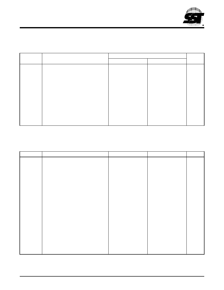
Concurrent Read/Write Operation
Dual bank architecture of SST36VF1601 device allows the
Concurrent Read/Write operation whereby the user can
read from one bank while program or erase in the other
bank. This operation can be used when the user needs to
read system code in one bank while updating data in the
other bank.
Note: For the purposes of this table, write means to perform Block-,
Sector-, or Chip-Erase or Word-Program operations as appli-
cable to the appropriate bank.
Read Operation
The Read operation of the SST36VF1601 is controlled
by CE# and OE#, both have to be low for the system to
obtain data from the outputs. CE# is used for device
selection. When CE# is high, the chip is deselected
and only standby power is consumed. OE# is the out-
put control and is used to gate data on the output pins.
The data bus is in high impedance state when either
CE# or OE# is high. Refer to the Read cycle timing
diagram for further details (Figure 4).
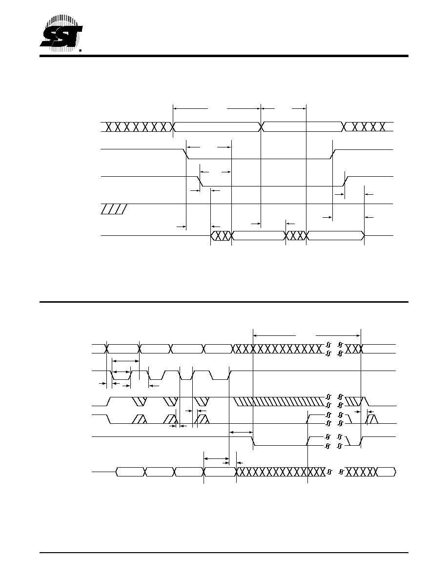
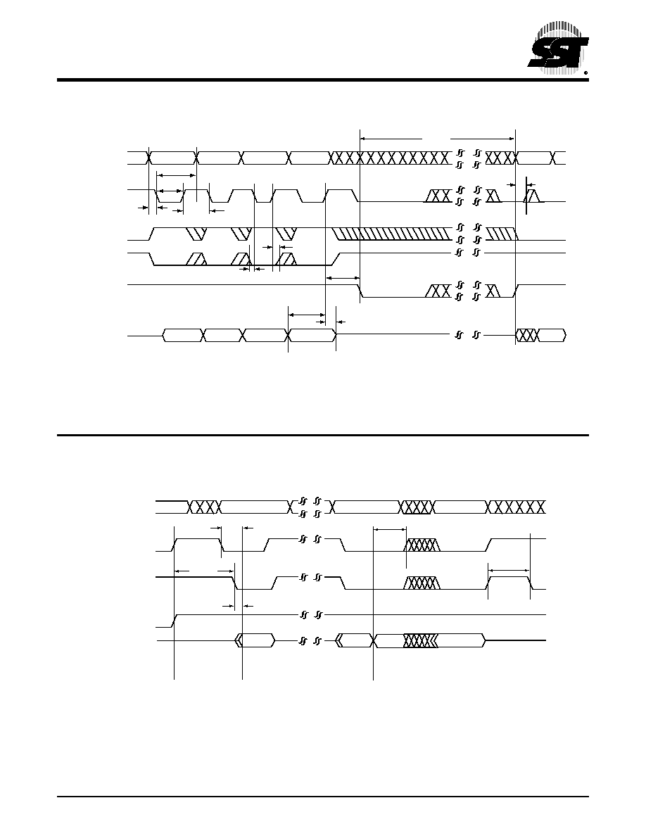
Word-Program Operation
The SST36VF1601 is programmed on a word-by-word
basis. Before programming, one must ensure that the sec-
tor, in which the word which is being programmed exists, is
fully erased. The Program operation consists of three
steps. The first step is the three-byte load sequence for
Software Data Protection. The second step is to load word
address and word data. During the Word-Program opera-
tion, the addresses are latched on the falling edge of either
CE# or WE#, whichever occurs last. The data is latched
on the rising edge of either CE# or WE#, whichever occurs
first. The third step is the internal Program operation which
is initiated after the rising edge of the fourth WE# or CE#,
whichever occurs first. The Program operation, once initi-
ated, will be completed typically within 10 µs. See Figures
5 and 6 for WE# and CE# controlled Program operation
timing diagrams and Figure 19 for flowcharts. During the
Program operation, the only valid reads are Data# Polling
and Toggle Bit. During the internal Program operation, the
host is free to perform additional tasks. Any commands
issued during the internal Program operation are ignored.
After detecting the completion of a Word-Program
operation (either through RY/BY# line, Data# Polling,
or Toggle Bit), the host must keep CE# signal low for a
minimum duration of Program Recovery Time
(T
PR
= ~1 µs) before valid data can be read correctly.
Please see Figures 5 through 8 for corresponding AC
timing diagrams.
Sector- (Block-) Erase Operation
The Sector- (Block-) Erase operation allows the system to
erase the device on a sector-by-sector (or block-by-block)
basis. The SST36VF1601 offers both Sector-Erase and
Block-Erase mode. The sector architecture is based on
uniform sector size of 1 KWord. The Block-Erase mode is
based on uniform block size of 32 KWord. The Sector-
Erase operation is initiated by executing a six-byte com-
mand sequence with Sector-Erase command (30H) and
sector address (SA) in the last bus cycle. The Block-Erase
operation is initiated by executing a six-byte command
sequence with Block-Erase command (50H) and block
address (BA) in the last bus cycle. The sector or block
address is latched on the falling edge of the sixth WE#
pulse, while the command (30H or 50H) is latched on the
rising edge of the sixth WE# pulse. The internal Erase
operation begins after the sixth WE# pulse. See Figures 10
and 11 for timing waveforms. Any commands issued during
the Sector- or Block-Erase operation are ignored.
C
ONCURRENT
R
EAD
/W
RITE
S
TATE
Bank 1
Bank 2
Read
No Operation
Read
Write
Write
Read
Write
No Operation
No Operation
Read
No Operation
Write
Data Sheet
16 Mbit Concurrent SuperFlash
SST36VF1601
3
©2002 Silicon Storage Technology, Inc.
S71142-07-000
5/02
373
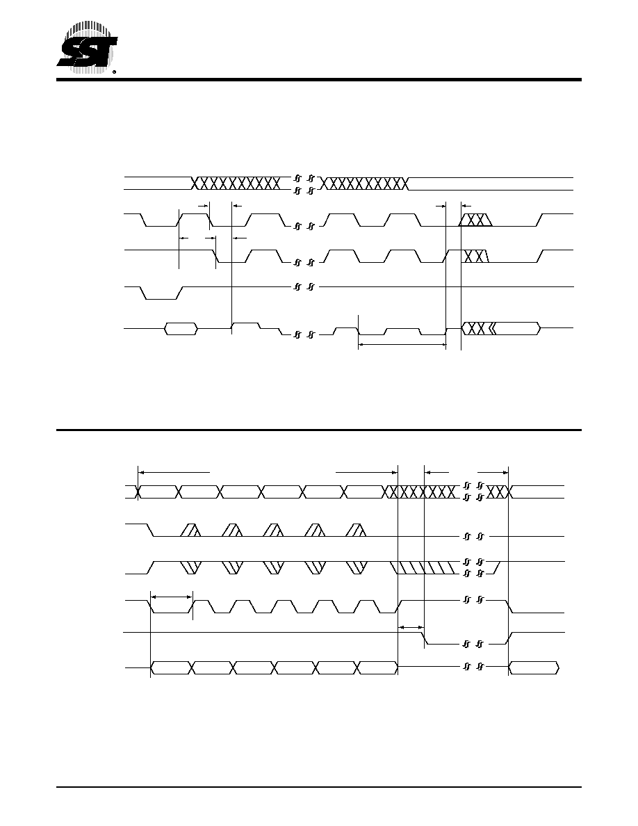
Chip-Erase Operation
The SST36VF1601 provides a Chip-Erase operation,
which allows the user to erase all unprotected sectors/
blocks to the "1" state. This is useful when the device must
be quickly erased.
The Chip-Erase operation is initiated by executing a six-
byte command sequence with Chip-Erase command (10H)
at address 5555H in the last byte sequence. The Erase
operation begins with the rising edge of the sixth WE# or
CE#, whichever occurs first. During the Erase operation,
the only valid Read is Toggle Bit or Data# Polling. See
Table 4 for the command sequence, Figure 9 for timing dia-
gram, and Figure 22 for the flowchart. Any commands
issued during the Chip-Erase operation are ignored.
Write Operation Status Detection
The SST36VF1601 provides one hardware and two soft-
ware means to detect the completion of a Write (Program
or Erase) cycle, in order to optimize the system Write cycle
time. The hardware detection uses the Ready/Busy# (RY/
BY#) output pin. The software detection includes two status
bits: Data# Polling (DQ
7
) and Toggle Bit (DQ
6
). The End-of-
Write detection mode is enabled after the rising edge of
WE#, which initiates the internal Program or Erase opera-
tion.
The actual completion of the nonvolatile write is asynchro-
nous with the system; therefore, either a Ready/Busy# (RY/
BY#), a Data# Polling (DQ
7
) or Toggle Bit (DQ
6
) read may
be simultaneous with the completion of the Write cycle. If
this occurs, the system may possibly get an erroneous
result, i.e., valid data may appear to conflict with either DQ
7
or DQ
6
. In order to prevent spurious rejection, if an errone-
ous result occurs, the software routine should include a
loop to read the accessed location an additional two (2)
times. If both reads are valid, then the device has com-
pleted the Write cycle, otherwise the rejection is valid.
Ready/Busy# (RY/BY#)
The SST36VF1601 includes a Ready/Busy# (RY/BY#)
output signal. RY/BY# is actively pulled low while during an
internal Erase or Program operation is in progress. RY/BY#
is an open drain output that allows several devices to be
tied in parallel to V
DD
via an external pull up resistor. RY/
BY# is high impedance whenever CE# is high or RST# is
low. There is a 1 µs bus recovery time (T
BR
) required before
valid data can be read on the data bus. New commands
can be entered immediately after RY/BY# goes high.
Data# Polling (DQ
7
)
When the SST36VF1601 is in the internal Program opera-
tion, any attempt to read DQ
7
will produce the complement
of the true data. Once the Program operation is completed,
DQ
7
will produce true data. During internal Erase opera-
tion, any attempt to read DQ
7
will produce a `0'. Once the
internal Erase operation is completed, DQ
7
will produce a
`1'. The Data# Polling is valid after the rising edge of fourth
WE# (or CE#) pulse for Program operation. For Sector-,
Block-, or Chip-Erase, the Data# Polling is valid after the
rising edge of sixth WE# (or CE#) pulse. See Figure 7 for
Data# Polling (DQ
7
) timing diagram and Figure 20 for a
flowchart. There is a 1 µs bus recovery time (T
BR
) required
before valid data can be read on the data bus. New com-
mands can be entered immediately after DQ
7
becomes
true data.
Toggle Bit (DQ
6
)
During the internal Program or Erase operation, any con-
secutive attempts to read DQ
6
will produce alternating 1s
and 0s, i.e., toggling between 1 and 0. When the internal
Program or Erase operation is completed, the DQ
6
bit will
stop toggling. The Toggle Bit is valid after the rising edge of
fourth WE# (or CE#) pulse for Program operation. For Sec-
tor-, Block- or Chip-Erase, the Toggle Bit is valid after the
rising edge of sixth WE# (or CE#) pulse. See Figure 8 for
Toggle Bit timing diagram and Figure 20 for a flowchart.
There is a 1 µs bus recovery time (T
BR
) required before
valid data can be read on the data bus. New commands
can be entered immediately after DQ
6
no longer toggles.
Data Protection
The SST36VF1601 provides both hardware and software
features to protect nonvolatile data from inadvertent writes.
Hardware Data Protection
Noise/Glitch Protection: A WE# or CE# pulse of less than 5
ns will not initiate a Write cycle.
V
DD
Power Up/Down Detection: The Write operation is
inhibited when V
DD
is less than 1.5V.
Write Inhibit Mode: Forcing OE# low, CE# high, or WE#
high will inhibit the Write operation. This prevents inadvert-
ent writes during power-up or power-down.
4
Data Sheet
16 Mbit Concurrent SuperFlash
SST36VF1601
©2002 Silicon Storage Technology, Inc.
S71142-07-000
5/02
373
Hardware Block Protection
The SST36VF1601 provides a hardware block protection
which protects the outermost 4 KWord in the larger bank.
The block is protected when WP# is held low. See Figure 1
for Block-Protection location.
A user can disable block protection by driving WP# high
thus allowing erase or program of data into the protected
sectors. WP# must be held high prior to issuing the write
command and remain stable until after the entire Write
operation has completed.
Hardware Reset (RST#)
The RST# pin provides a hardware method of resetting the
device to read array data. When the RST# pin is held low
for at least T
RP,
any in-progress operation will terminate and
return to Read mode (see Figure 16). When no internal
Program/Erase operation is in progress, a minimum period
of T
RHR
is required after RST# is driven high before a valid
Read can take place (see Figure 15).
The Erase operation that has been interrupted needs to be
reinitiated after the device resumes normal operation mode
to ensure data integrity.
Software Data Protection (SDP)
The SST36VF1601 provides the JEDEC standard Soft-
ware Data Protection scheme for all data alteration opera-
tions, i.e., Program and Erase. Any Program operation
requires the inclusion of the three-byte sequence. The
three-byte load sequence is used to initiate the Program
operation, providing optimal protection from inadvertent
Write operations, e.g., during the system power-up or
power-down. Any Erase operation requires the inclusion of
six-byte sequence. The SST36VF1601 is shipped with the
Software Data Protection permanently enabled. See Table
4 for the specific software command codes. During SDP
command sequence, invalid commands will abort the
device to Read mode within T
RC.
The contents of DQ
15
-
DQ
8
can be V
IL
or V
IH
, but no other value during any SDP
command sequence.
Common Flash Memory Interface (CFI)
The SST36VF1601 also contains the CFI information to
describe the characteristics of the device. In order to enter
the CFI Query mode, the system must write three-byte
sequence, same as Software ID Entry command with 98H
(CFI Query command) to address 5555H in the last byte
sequence. Once the device enters the CFI Query mode,
the system can read CFI data at the addresses given in
Tables 5 through 7. The system must write the CFI Exit
command to return to Read mode from the CFI Query
mode.
Product Identification
The Product Identification mode identifies the device and
manufacturer. For details, see Table 4 for software opera-
tion, Figure 12 for the Software ID Entry and Read timing
diagram and Figure 21 for the Software ID Entry command
sequence flowchart.
Product Identification Mode
Exit/CFI Mode Exit
In order to return to the standard Read mode, the Soft-
ware Product Identification mode must be exited. Exit is
accomplished by issuing the Software ID Exit command
sequence, which returns the device to the Read mode.
This command may also be used to reset the device to the
Read mode after any inadvertent transient condition that
apparently causes the device to behave abnormally, e.g.,
not read correctly. Please note that the Software ID Exit/
CFI Exit command is ignored during an internal Program
or Erase operation. See Table 4 for the software command
code, Figure 14 for timing waveform and Figure 21 for a
flowchart.
TABLE
1: P
RODUCT
I
DENTIFICATION
Word
Data
Manufacturer's ID
0000H
00BFH
Device ID
SST36VF1601
0001H
2761H
T1.1 373
Data Sheet
16 Mbit Concurrent SuperFlash
SST36VF1601
5
©2002 Silicon Storage Technology, Inc.
S71142-07-000
5/02
373
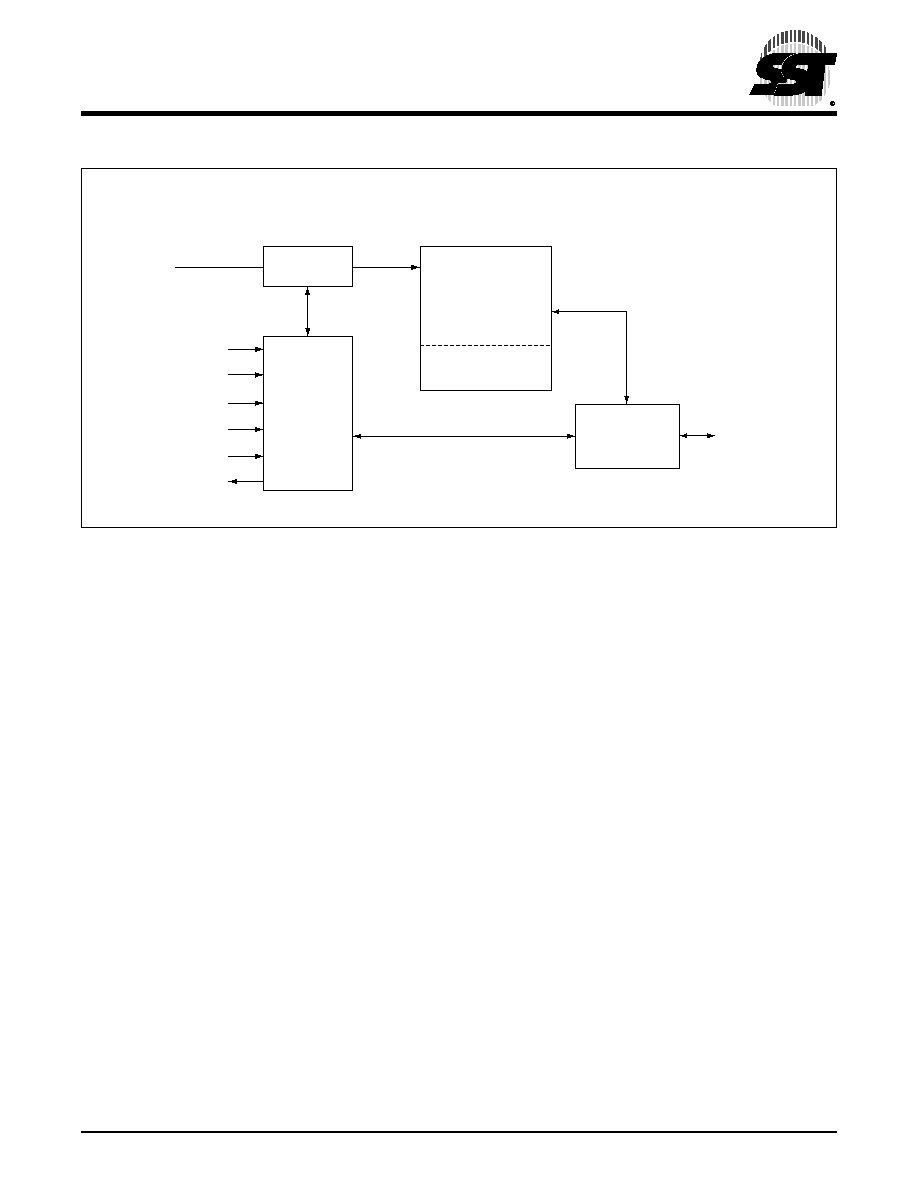
373 ILL B37.5
SuperFlash Memory
12 Mbit Bank
I/O Buffers
SuperFlash Memory
4 Mbit Bank
Memory
Address
DQ15 - DQ0
CE#
WP#
WE#
OE#
Control
Logic
RST#
RY/BY#
Address
Buffers
(4 KWord Sector Protection)
F
UNCTIONAL
B
LOCK
D
IAGRAM
6
Data Sheet
16 Mbit Concurrent SuperFlash
SST36VF1601
©2002 Silicon Storage Technology, Inc.
S71142-07-000
5/02
373
FIGURE 1: SST36VF1601, 1 M
BIT
X
16 C
ONCURRENT
S
UPER
F
LASH
D
UAL
-B
ANK
M
EMORY
O
RGANIZATION
FFFFFH
F8000H
Block 31
F7FFFH
F0000H
Block 30
EFFFFH
E8000H
Block 29
E7FFFH
E0000H
Block 28
DFFFFH
D8000H
Block 27
D7FFFH
D0000H
Block 26
CFFFFH
C8000H
Block 25
C7FFFH
C0000H
Block 24
Bank 2
BFFFFH
B8000H
Block 23
B7FFFH
B0000H
Block 22
AFFFFH
A8000H
Block 21
A7FFFH
A0000H
Block 20
9FFFFH
98000H
Block 19
97FFFH
90000H
Block 18
8FFFFH
88000H
Block 17
87FFFH
80000H
Block 16
7FFFFH
78000H
Block 15
77FFFH
70000H
Block 14
6FFFFH
68000H
Block 13
67FFFH
60000H
Block 12
5FFFFH
58000H
Block 11
57FFFH
50000H
Block 10
4FFFFH
48000H
Block 9
47FFFH
40000H
Block 8
3FFFFH
38000H
Block 7
37FFFH
30000H
Block 6
2FFFFH
28000H
Block 5
27FFFH
20000H
Block 4
1FFFFH
18000H
Block 3
17FFFH
10000H
Block 2
00FFFFH
008000H
Block 1
007FFFH
001000H
000FFFH
000000H
Block 0
Bank 1
Bottom Sector Protection; 32 KWord Blocks; 1 KWord Sectors
4 KWord Sector Protection
(4- 1 KWord Sectors)
373 ILL F38.2
Data Sheet
16 Mbit Concurrent SuperFlash
SST36VF1601
7
©2002 Silicon Storage Technology, Inc.
S71142-07-000
5/02
373
FIGURE 2: P
IN
A
SSIGNMENTS
FOR
48-
LEAD
TSOP (12
MM
X
20
MM
)
FIGURE 3: P
IN
A
SSIGNMENTS
FOR
48-
BALL
TFBGA (8
MM
X
10
MM
)
A15
A14
A13
A12
A11
A10
A9
A8
A19
NC
WE#
RST#
NC
WP#
RY/BY#
A18
A17
A7
A6
A5
A4
A3
A2
A1
1
2
3
4
5
6
7
8
9
10
11
12
13
14
15
16
17
18
19
20
21
22
23
24
A16
NC
VSS
DQ15
DQ7
DQ14
DQ6
DQ13
DQ5
DQ12
DQ4
VDD
DQ11
DQ3
DQ10
DQ2
DQ9
DQ1
DQ8
DQ0
OE#
VSS
CE#
A0
48
47
46
45
44
43
42
41
40
39
38
37
36
35
34
33
32
31
30
29
28
27
26
25
373 ILL F01b.3
Standard Pinout
Top View
Die Up
A13
A9
WE#
RY/BY#
A7
A3
A12
A8
RST#
WP#
A17
A4
A14
A10
NC
A18
A6
A2
A15
A11
A19
NC
A5
A1
A16
DQ7
DQ5
DQ2
DQ0
A0
NC
DQ14
DQ12
DQ10
DQ8
CE#
DQ15
DQ13
VDD
DQ11
DQ9
OE#
VSS
DQ6
DQ4
DQ3
DQ1
VSS
373 ILL F01a.7
SST36VF1601
TOP VIEW (balls facing down)
6
5
4
3
2
1
A B C D E F G H
8
Data Sheet
16 Mbit Concurrent SuperFlash
SST36VF1601
©2002 Silicon Storage Technology, Inc.
S71142-07-000
5/02
373
TABLE
2: P
IN
D
ESCRIPTION
Symbol
Name
Functions
A
19
-A
0
Address Inputs
To provide memory addresses. During Sector-Erase and Hardware Sector Protection,
A
19
-A
10
address lines will select the sector. During Block-Erase A
19
-A
15
address lines
will select the block.
DQ
15
-DQ
0
Data Input/output
To output data during Read cycles and receive input data during Write cycles
Data is internally latched during a Write cycle. The outputs are in tri-state when OE#
or CE# is high.
CE#
Chip Enable
To activate the device when CE# is low.
OE#
Output Enable
To gate the data output buffers
WE#
Write Enable
To control the Write operations
RST#
Hardware Reset
To reset and return the device to Read mode
RY/BY#
Ready/Busy#
To output the status of a Program or Erase Operation
RY/BY# is a open drain output, so a 10K
- 100K pull-up resistor is required to allow
RY/BY# to transition high indicating the device is ready to read.
WP#
Write Protect
To protect and unprotect the bottom 4 sectors from Erase or Program operation.
V
DD
Power Supply
To provide 2.7-3.6V power supply voltage
V
SS
Ground
NC
No Connection
Unconnected pins
T2.6 373
TABLE
3: O
PERATION
M
ODES
S
ELECTION
Mode
CE#
OE#
WE#
DQ
Address
Read
V
IL
V
IL
V
IH
D
OUT
A
IN
Program
V
IL
V
IH
V
IL
D
IN
A
IN
Erase
V
IL
V
IH
V
IL
X
1
1. X can be VIL or VIH, but no other value.
Sector or block address,
XXH for Chip-Erase
Standby V
IH
X
X
High Z
X
Write Inhibit
X
V
IL
X
High Z / D
OUT
X
X
X
V
IH
High Z / D
OUT
X
Product Identification
Software Mode
V
IL
V
IL
V
IH
Manufacturer's ID (00BFH)
See Table 4
Device ID
2
2. Device ID = 2761H
T3.6 373
Data Sheet
16 Mbit Concurrent SuperFlash
SST36VF1601
9
©2002 Silicon Storage Technology, Inc.
S71142-07-000
5/02
373
TABLE
4: S
OFTWARE
C
OMMAND
S
EQUENCE
Command
Sequence
1st Bus
Write Cycle
2nd Bus
Write Cycle
3rd Bus
Write Cycle
4th Bus
Write Cycle
5th Bus
Write Cycle
6th Bus
Write Cycle
Addr
1
Data
2
Addr
1
Data
2
Addr
1
Data
2
Addr
1
Data
2
Addr
1
Data
2
Addr
1
Data
2
Word-Program
5555H
AAH
2AAAH
55H
5555H
A0H
WA
3
Data
Sector-Erase
5555H
AAH
2AAAH
55H
5555H
80H
5555H
AAH
2AAAH
55H
SA
X
4
30H
Block-Erase
5555H
AAH
2AAAH
55H
5555H
80H
5555H
AAH
2AAAH
55H
BA
X
4
50H
Chip-Erase
5555H
AAH
2AAAH
55H
5555H
80H
5555H
AAH
2AAAH
55H
5555H
10H
Software ID Entry
5,6
5555H
AAH
2AAAH
55H
5555H
90H
CFI Query Entry
5555H
AAH
2AAAH
55H
5555H
98H
Software ID Exit/
CFI Exit
5555H
AAH
2AAAH
55H
5555H
F0H
T4.4 373
1. Address format A
14
-A
0
(Hex), Addresses A
19
- A
15
can be V
IL
or V
IH
, but no other value, for the Command sequence.
2. DQ
15
-DQ
8
can be V
IL
or V
IH
, but no other value, for the Command sequence
3. WA = Program word address
4. SA
X
for Sector-Erase; uses A
19
-A
10
address lines
BA
X
for Block-Erase; uses A
19
-A
15
address lines
5. The device does not remain in Software Product Identification mode if powered down.
6. With A
19
-A
1
= 0;
SST Manufacturer's ID = 00BFH, is read with A
0
= 0
SST36VF1601 Device ID = 2761H, is read with A
0
= 1
TABLE
5: CFI Q
UERY
I
DENTIFICATION
S
TRING1
1. Refer to CFI publication 100 for more details.
Address
Data
Data
10H
0051H
Query Unique ASCII string "QRY"
11H
0052H
12H
0059H
13H
0001H
Primary OEM command set
14H
0007H
15H
0000H
Address for Primary Extended Table
16H
0000H
17H
0000H
Alternate OEM command set (00H = none exists)
18H
0000H
19H
0000H
Address for Alternate OEM extended Table (00H = none exits)
1AH
0000H
T5.0 373
10
Data Sheet
16 Mbit Concurrent SuperFlash
SST36VF1601
©2002 Silicon Storage Technology, Inc.
S71142-07-000
5/02
373
TABLE
6: S
YSTEM
I
NTERFACE
I
NFORMATION
Address
Data
Data
1BH
0027H
V
DD
Min (Program/Erase)
DQ
7
-DQ
4
: Volts, DQ
3
-DQ
0
: 100 millivolts
1CH
0036H
V
DD
Max (Program/Erase)
DQ
7
-DQ
4
: Volts, DQ
3
-DQ
0
: 100 millivolts
1DH
0000H
V
PP
min (00H = no V
PP
pin)
1EH
0000H
V
PP
max (00H = no V
PP
pin)
1FH
0004H
Typical time out for Word-Program 2
N
µs (2
4
= 16 µs)
20H
0000H
Typical time out for min size buffer program 2
N
µs (00H = not supported)
21H
0004H
Typical time out for individual Sector/Block-Erase 2
N
ms (2
4
= 16 ms)
22H
0006H
Typical time out for Chip-Erase 2
N
ms (2
6
= 64 ms)
23H
0001H
Maximum time out for Word-Program 2
N
times typical (2
1
x 2
4
= 32 µs)
24H
0000H
Maximum time out for buffer program 2
N
times typical
25H
0001H
Maximum time out for individual Sector/Block-Erase 2
N
times typical (2
1
x 2
4
= 32 ms)
26H
0001H
Maximum time out for Chip-Erase 2
N
times typical (2
1
x 2
6
= 128 ms)
T6.0 373
TABLE
7: D
EVICE
G
EOMETRY
I
NFORMATION
Address
Data
Data
27H
0015H
Device size = 2
N
Bytes (15H = 21; 2
21
= 2 MByte)
28H
0001H
Flash Device Interface description; 0001H = x16-only asynchronous interface
29H
0000H
2AH
0000H
Maximum number of bytes in multi-byte write = 2
N
(00H = not supported)
2BH
0000H
2CH
0002H
Number of Erase Sector/Block sizes supported by device
2DH
00FFH
Sector Information (y + 1 = Number of sectors; z x 256B = sector size)
2EH
0003H
y = 1023 + 1 = 1024 sectors (03FFH = 1023)
2FH
0008H
30H
0000H
z = 8 x 256 Bytes = 2 KByte/sector (0008H = 8)
31H
003FH
Block Information (y + 1 = Number of blocks; z x 256B = block size)
32H
0000H
y = 31 + 1 = 32 blocks (001FH = 31)
33H
0000H
34H
0001H
z = 256 x 256 Bytes = 64 KByte/block (0100H = 256)
T7.4 373
Data Sheet
16 Mbit Concurrent SuperFlash
SST36VF1601
11
©2002 Silicon Storage Technology, Inc.
S71142-07-000
5/02
373
Absolute Maximum Stress Ratings (Applied conditions greater than those listed under "Absolute Maximum
Stress Ratings" may cause permanent damage to the device. This is a stress rating only and functional operation
of the device at these conditions or conditions greater than those defined in the operational sections of this data
sheet is not implied. Exposure to absolute maximum stress rating conditions may affect device reliability.)
Temperature Under Bias . . . . . . . . . . . . . . . . . . . . . . . . . . . . . . . . . . . . . . . . . . . . . . . . . . . . . . . . . -55∞C to +125∞C
Storage Temperature . . . . . . . . . . . . . . . . . . . . . . . . . . . . . . . . . . . . . . . . . . . . . . . . . . . . . . . . . . . -65∞C to +150∞C
D. C. Voltage on Any Pin to Ground Potential . . . . . . . . . . . . . . . . . . . . . . . . . . . . . . . . . . . . . . . . -0.5V to V
DD
+0.5V
Transient Voltage (<20 ns) on Any Pin to Ground Potential . . . . . . . . . . . . . . . . . . . . . . . . . . . . . -2.0V to V
DD
+2.0V
Package Power Dissipation Capability (Ta = 25∞C) . . . . . . . . . . . . . . . . . . . . . . . . . . . . . . . . . . . . . . . . . . . . . . 1.0W
Surface Mount Lead Soldering Temperature (3 Seconds) . . . . . . . . . . . . . . . . . . . . . . . . . . . . . . . . . . . . . . . . 240∞C
Output Short Circuit Current . . . . . . . . . . . . . . . . . . . . . . . . . . . . . . . . . . . . . . . . . . . . . . . . . . . . . . . . . . . . . . 50 mA
O
PERATING
R
ANGE
:
Range
Ambient Temp
V
DD
Commercial
0∞C to +70∞C
2.7-3.6V
Extended
-20∞C to +85∞C
2.7-3.6V
AC C
ONDITIONS
OF
T
EST
Input Rise/Fall Time . . . . . . . . . . . . . . 5 ns
Output Load . . . . . . . . . . . . . . . . . . . . C
L
= 30 pF
See Figures 17 and 18
12
Data Sheet
16 Mbit Concurrent SuperFlash
SST36VF1601
©2002 Silicon Storage Technology, Inc.
S71142-07-000
5/02
373
TABLE
8: DC O
PERATING
C
HARACTERISTICS
V
DD
= 2.7-3.6V
Symbol
Parameter
Limits
Test Conditions
Min
Max
Units
I
DD
Active V
DD
Current
Address input=V
IL
/V
IH
, at f=1/T
RC
Min,
V
DD
=V
DD
Max
Read
35
mA
CE#=OE#=V
IL
, WE#=V
IH
, all I/Os open
Program and Erase
40
mA
CE#=V
IL
, OE#=V
IH
Concurrent Read/Write
75
mA
I
SB
Standby V
DD
Current
20
µA
CE#=V
IHC
, V
DD
=V
DD
Max
I
RT
Reset V
DD
Current
20
µA
RST# = V
SS
± 0.3V
I
LI
Input Leakage Current
1
µA
V
IN
=GND to V
DD
, V
DD
=V
DD
Max
I
LO
Output Leakage Current
1
µA
V
OUT
=GND to V
DD
, V
DD
=V
DD
Max
V
IL
Input Low Voltage
0.8
V
V
DD
=V
DD
Min
V
ILC
Input Low Voltage (CMOS)
0.3
V
V
DD
=V
DD
Max
V
IH
Input High Voltage
0.7 V
DD
V
V
DD
=V
DD
Max
V
IHC
Input High Voltage (CMOS)
V
DD
-0.3
V
V
DD
=V
DD
Max
V
OL
Output Low Voltage
0.2
V
I
OL
=100 µA, V
DD
=V
DD
Min
V
OH
Output High Voltage
V
DD
-0.2
V
I
OH
=-100 µA, V
DD
=V
DD
Min
T8.6 373
TABLE
9: R
ECOMMENDED
S
YSTEM
P
OWER
-
UP
T
IMINGS
Symbol
Parameter
Minimum
Units
T
PU-READ
1
1. This parameter is measured only for initial qualification and after a design or process change that could affect this parameter.
Power-up to Read Operation
100
µs
T
PU-WRITE
1
Power-up to Write Operation
100
µs
T9.2 373
TABLE 10: C
APACITANCE
(Ta = 25∞C, f=1 Mhz, other pins open)
Parameter
Description
Test Condition
Maximum
C
I/O
1
1. This parameter is measured only for initial qualification and after a design or process change that could affect this parameter.
I/O Pin Capacitance
V
I/O
= 0V
10 pF
C
IN
1
Input Capacitance
V
IN
= 0V
10 pF
T10.0 373
TABLE 11: R
ELIABILITY
C
HARACTERISTICS
Symbol
Parameter
Minimum Specification
Units
Test Method
N
END
1
1. This parameter is measured only for initial qualification and after a design or process change that could affect this parameter.
Endurance
10,000
Cycles
JEDEC Standard A117
T
DR
1
Data Retention
100
Years
JEDEC Standard A103
I
LTH
1
Latch Up
100 + I
DD
mA
JEDEC Standard 78
T11.1 373
Data Sheet
16 Mbit Concurrent SuperFlash
SST36VF1601
13
©2002 Silicon Storage Technology, Inc.
S71142-07-000
5/02
373
AC CHARACTERISTICS
TABLE 12: R
EAD
C
YCLE
T
IMING
P
ARAMETERS
V
DD
= 2.7-3.6V
Symbol
Parameter
SST36VF1601-70
Units
Min
Max
T
RC
Read Cycle Time
70
ns
T
CE
Chip Enable Access Time
70
ns
T
AA
Address Access Time
70
ns
T
OE
Output Enable Access Time
35
ns
T
CLZ
1
1. This parameter is measured only for initial qualification and after a design or process change that could affect this parameter.
CE# Low to Active Output
0
ns
T
OLZ
1
OE# Low to Active Output
0
ns
T
CHZ
1
CE# High to High-Z Output
20
ns
T
OHZ
1
OE# High to High-Z Output
20
ns
T
OH
1
Output Hold from Address Change
0
ns
T
RP
1
RST# Pulse Width
500
ns
T
RHR
1
RST# High before Read
50
ns
T
RY
1,2
2. This parameter applies to Sector-Erase, Block-Erase and Program operations. This parameter does not apply to Chip-Erase opera-
tions.
RST# Pin Low to Read Mode
150
µs
T12.9 373
TABLE 13: P
ROGRAM
/E
RASE
C
YCLE
T
IMING
P
ARAMETERS
Symbol
Parameter
Min
Max
Units
T
BP
Word-Program Time
20
µs
T
AS
Address Setup Time
0
ns
T
AH
Address Hold Time
40
ns
T
CS
WE# and CE# Setup Time
0
ns
T
CH
WE# and CE# Hold Time
0
ns
T
OES
OE# High Setup Time
0
ns
T
OEH
OE# High Hold Time
10
ns
T
CP
CE# Pulse Width
40
ns
T
WP
WE# Pulse Width
40
ns
T
WPH
1
1. This parameter is measured only for initial qualification and after a design or process change that could affect this parameter.
WE# Pulse Width High
30
ns
T
CPH
1
CE# Pulse Width High
30
ns
T
DS
Data Setup Time
30
ns
T
DH
1
Data Hold Time
0
ns
T
IDA
1
Software ID Access and Exit Time
150
ns
T
SE
Sector-Erase
25
ms
T
BE
Block-Erase
25
ms
T
SCE
Chip-Erase
100
ms
T
BY
1
RY/BY# Delay Time
90
ns
T
PR
Program Recovery Time
1
µs
T13.7 373
14
Data Sheet
16 Mbit Concurrent SuperFlash
SST36VF1601
©2002 Silicon Storage Technology, Inc.
S71142-07-000
5/02
373
FIGURE 4: R
EAD
C
YCLE
T
IMING
D
IAGRAM
FIGURE 5: WE# C
ONTROLLED
W
ORD
-P
ROGRAM
C
YCLE
T
IMING
D
IAGRAM
373 ILL F22.1
ADDRESSES
DQ15-0
WE#
OE#
CE#
TCE
TRC
TAA
TOE
TOLZ
VIH
HIGH-Z
TCLZ
TOH
TCHZ
HIGH-Z
DATA VALID
DATA VALID
TOHZ
373 ILL F23.15
ADDRESSES
DQ
15-0
T
CPH
T
DS
T
CP
T
AH
T
AS
T
CH
T
CS
CE#
5555
2AAA
5555
ADDR
XXAA
XX55
XXA0
DATA
WORD
(ADDR/DATA)
OE#
WE#
T
BP
RY/BY#
T
BY
T
PR
Note: X can be V
IL
or V
IH
, but no other value.
VALID
T
DH
Data Sheet
16 Mbit Concurrent SuperFlash
SST36VF1601
15
©2002 Silicon Storage Technology, Inc.
S71142-07-000
5/02
373
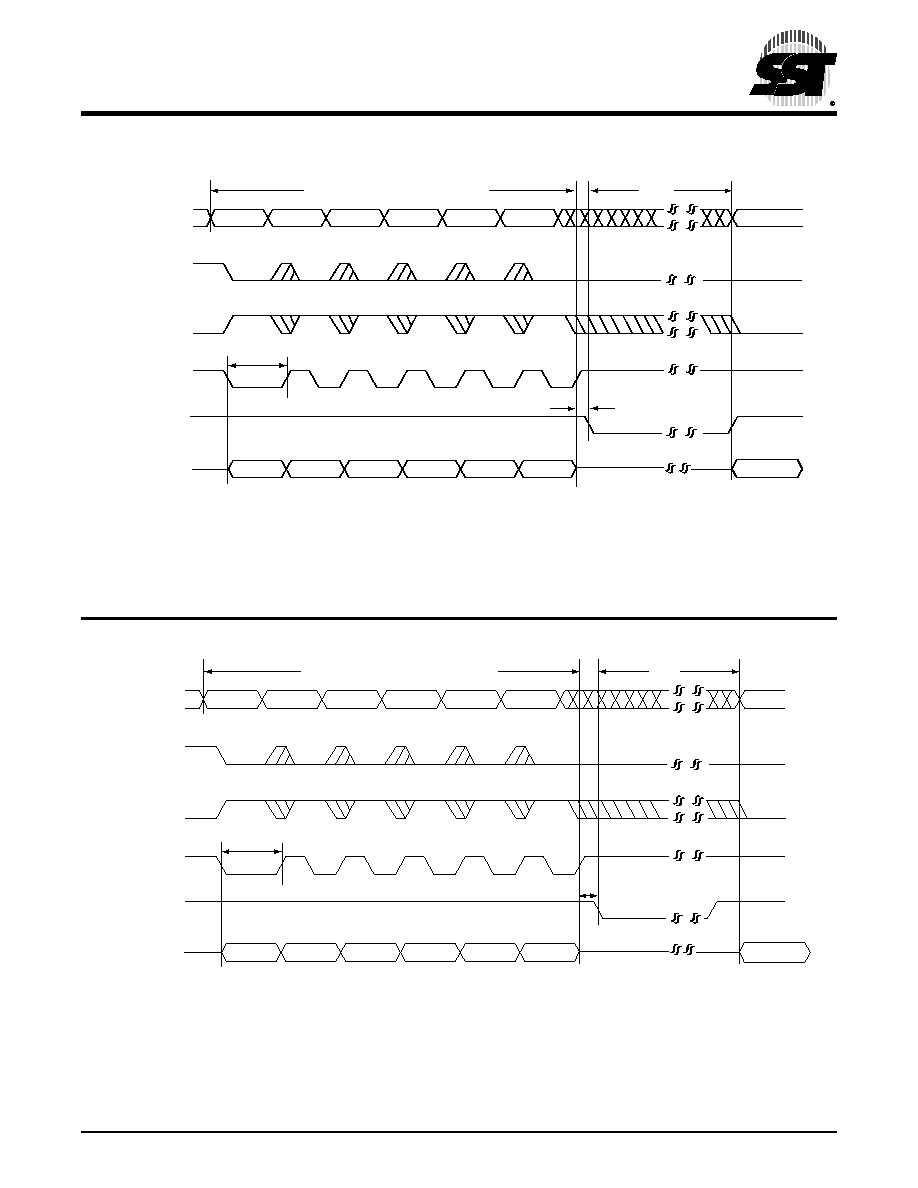
FIGURE 6: CE# C
ONTROLLED
W
ORD
-P
ROGRAM
C
YCLE
T
IMING
D
IAGRAM
FIGURE 7: D
ATA
# P
OLLING
T
IMING
D
IAGRAM
373 ILL F24.12
ADDRESSES
DQ
15-0
T
CPH
T
DS
T
CP
T
AH
T
AS
T
CH
T
CS
WE#
5555
2AAA
5555
ADDR
XXAA
XX55
XXA0
DATA
WORD
(ADDR/DATA)
OE#
CE#
T
BP
RY/BY#
T
BY
T
PR
Note: X can be V
IL
or V
IH
, but no other value.
VALID
T
DH
373 ILL F41.2
ADDRESSES
DQ7
DATA#
DATA#
WE#
OE#
CE#
T
OEH
T
OE
T
CE
T
OES
DATA
VALID DATA
T
PR
16
Data Sheet
16 Mbit Concurrent SuperFlash
SST36VF1601
©2002 Silicon Storage Technology, Inc.
S71142-07-000
5/02
373
FIGURE 8: T
OGGLE
B
IT
T
IMING
D
IAGRAM
FIGURE 9: WE# C
ONTROLLED
C
HIP
-E
RASE
T
IMING
D
IAGRAM
373 ILL F42.3
ADDRESSES
DQ6
WE#
OE#
CE#
TOE
TOEH
TCE
TWO READ CYCLES
WITH SAME OUTPUTS
VALID DATA
T
PR
373 ILL F27.8
ADDRESSES
DQ
15-0
WE#
5555
2AAA
2AAA
5555
5555
XX55
XX10
XX55
XXAA
XX80
XXAA
5555
OE#
CE#
SIX-BYTE CODE FOR CHIP-ERASE
T
SCE
T
WP
Note: This device also supports CE# controlled Chip-Erase operation. The WE# and CE# signals
are interchageable as long as minimum timings are met. (See Table 13)
X can be V
IL
or V
IH
, but no other value.
RY/BY#
T
BY
VALID
Data Sheet
16 Mbit Concurrent SuperFlash
SST36VF1601
17
©2002 Silicon Storage Technology, Inc.
S71142-07-000
5/02
373
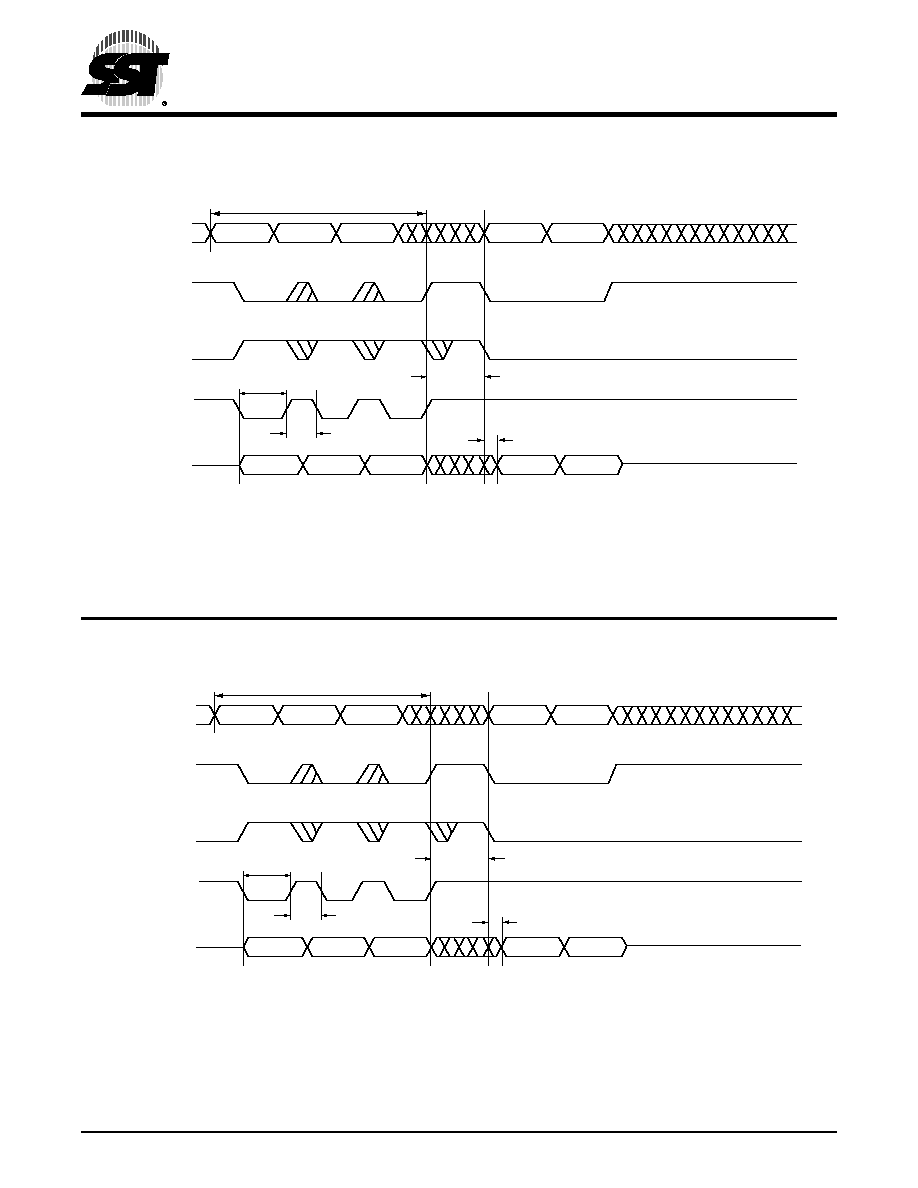
FIGURE 10: WE# C
ONTROLLED
B
LOCK
-E
RASE
T
IMING
D
IAGRAM
FIGURE 11: WE# C
ONTROLLED
S
ECTOR
-E
RASE
T
IMING
D
IAGRAM
373 ILL F28.10
ADDRESSES
DQ
15-0
WE#
5555
2AAA
2AAA
5555
5555
XX55
XX50
XX55
XXAA
XX80
XXAA
BAX
OE#
CE#
SIX-BYTE CODE FOR BLOCK-ERASE
T
BE
T
WP
Note: This device also supports CE# controlled Block-Erase operation. The WE# and CE#
signals are interchageable as long as minimum timings are met. (See Table 13)
BAX = Block Address
X can be V
IL
or V
IH
, but no other value.
RY/BY#
VALID
T
BY
373 ILL F29.10
ADDRESSES
DQ
15-0
WE#
5555
2AAA
2AAA
5555
5555
XX55
XX30
XX55
XXAA
XX80
XXAA
SAX
OE#
CE#
SIX-BYTE CODE FOR SECTOR-ERASE
T
SE
T
WP
Note: This device also supports CE# controlled Sector-Erase operation. The WE# and CE#
signals are interchageable as long as minimum timings are met. (See Table 13)
SA
X
= Sector Address
X can be V
IL
or V
IH
, but no other value.
RY/BY#
T
BY
VALID
18
Data Sheet
16 Mbit Concurrent SuperFlash
SST36VF1601
©2002 Silicon Storage Technology, Inc.
S71142-07-000
5/02
373
FIGURE 12: S
OFTWARE
ID E
NTRY
AND
R
EAD
FIGURE 13: CFI E
NTRY
AND
R
EAD
373 ILL F30.7
ADDRESSES
T
IDA
DQ
15-0
WE#
Device ID = 2761H for SST36VF1601
5555
2AAA
5555
0000
0001
OE#
CE#
THREE-BYTE SEQUENCE FOR
SOFTWARE ID ENTRY
T
WP
T
WPH
T
AA
00BF
Device ID
XX55
XXAA
XX90
Note: X can be V
IL
or V
IH
, but no other value.
373 ILL F31.3
ADDRESSES
T
IDA
DQ
15-0
WE#
5555
2AAA
5555
OE#
CE#
THREE-BYTE SEQUENCE FOR
CFI QUERY ENTRY
T
WP
T
WPH
T
AA
XX55
XXAA
XX98
Note: X can be V
IL
or V
IH
, but no other value.
Data Sheet
16 Mbit Concurrent SuperFlash
SST36VF1601
19
©2002 Silicon Storage Technology, Inc.
S71142-07-000
5/02
373
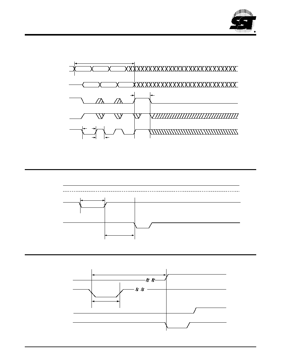
FIGURE 14: S
OFTWARE
ID E
XIT
/CFI E
XIT
FIGURE 15: RST# T
IMING
(
WHEN
NO
INTERNAL
OPERATION
IS
IN
PROGRESS
)
FIGURE 16: RST# T
IMING
(
DURING
S
ECTOR
-
OR
B
LOCK
-E
RASE
OPERATION
)
373 ILL F32.5
ADDRESSES
DQ
15-0
T
IDA
T
WP
T
WPH
WE#
5555
2AAA
5555
THREE-BYTE SEQUENCE FOR
SOFTWARE ID EXIT AND RESET
OE#
CE#
XXAA
XX55
XXF0
Note: X can be V
IL
or V
IH
, but no other value.
373 ILL F43.1
RY/BY#
0V
RST#
CE#/OE#
T
RP
T
RHR
373 ILL F44.3
RY/BY#
CE#
OE#
T
RP
T
RY
RST#
20
Data Sheet
16 Mbit Concurrent SuperFlash
SST36VF1601
©2002 Silicon Storage Technology, Inc.
S71142-07-000
5/02
373
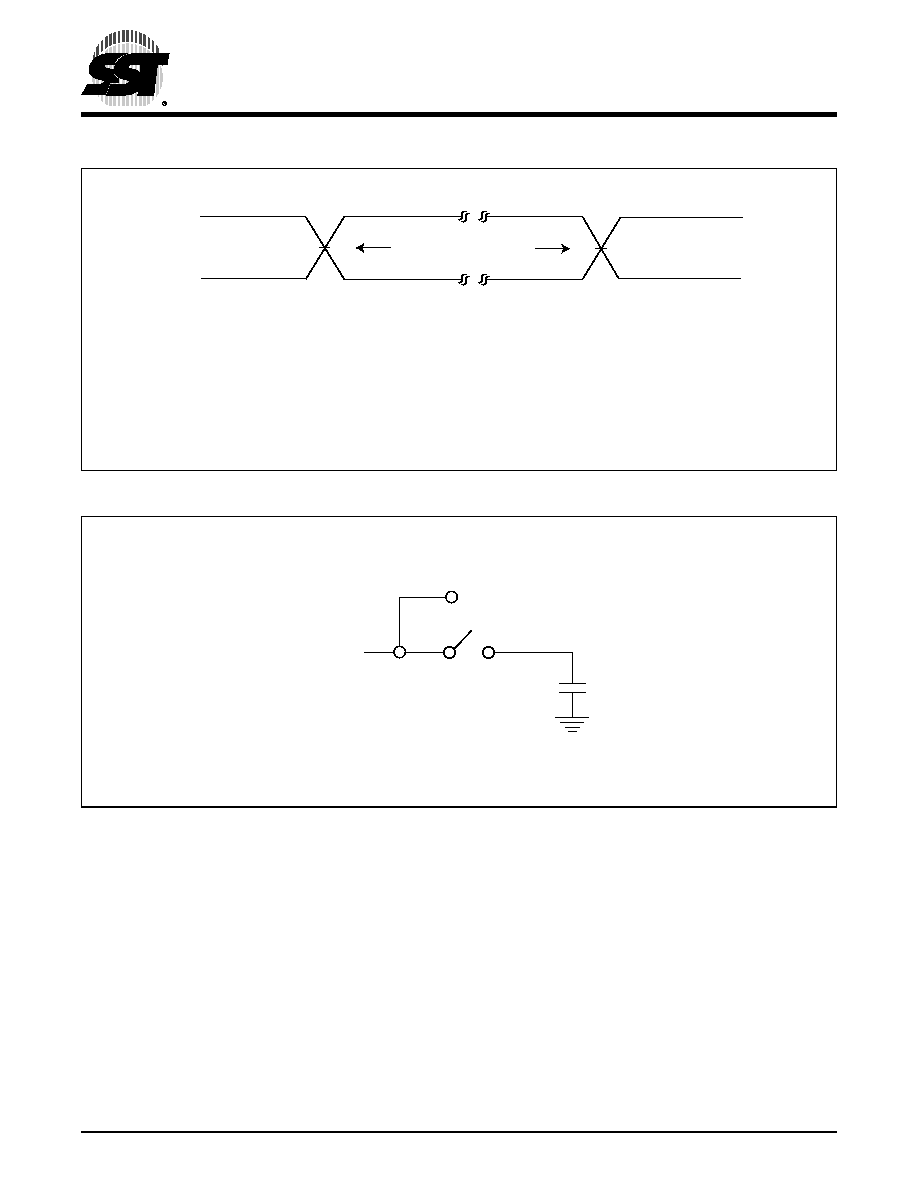
FIGURE 17: AC I
NPUT
/O
UTPUT
R
EFERENCE
W
AVEFORMS
FIGURE 18: A T
EST
L
OAD
E
XAMPLE
373 ILL F14.3
REFERENCE POINTS
OUTPUT
INPUT
VIT
VIHT
VILT
VOT
AC test inputs are driven at V
IHT
(0.9 V
DD
) for a logic "1" and V
ILT
(0.1 V
DD
) for a logic "0". Measurement reference points
for inputs and outputs are V
IT
(0.5 V
DD
) and V
OT
(0.5 V
DD
). Input rise and fall times (10%
90%) are <5 ns.
Note: V
IT
- V
INPUT
Test
V
OT
- V
OUTPUT
Test
V
IHT
- V
INPUT
HIGH Test
V
ILT
- V
INPUT
LOW Test
373 ILL F15.1
TO TESTER
TO DUT
CL
Data Sheet
16 Mbit Concurrent SuperFlash
SST36VF1601
21
©2002 Silicon Storage Technology, Inc.
S71142-07-000
5/02
373
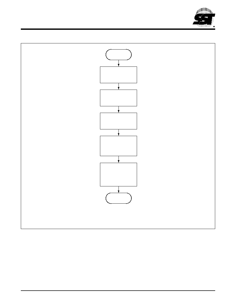
FIGURE 19: W
ORD
-P
ROGRAM
A
LGORITHM
373 ILL F33.3
Start
Load data: XXAAH
Address: 5555H
Load data: XX55H
Address: 2AAAH
Load data: XXA0H
Address: 5555H
Load Word
Address/Word
Data
Wait for end of
Program (TBP,
Data# Polling
bit, or Toggle bit
operation)
Program
Completed
Note: X can be VIL or VIH, but no other value.
22
Data Sheet
16 Mbit Concurrent SuperFlash
SST36VF1601
©2002 Silicon Storage Technology, Inc.
S71142-07-000
5/02
373
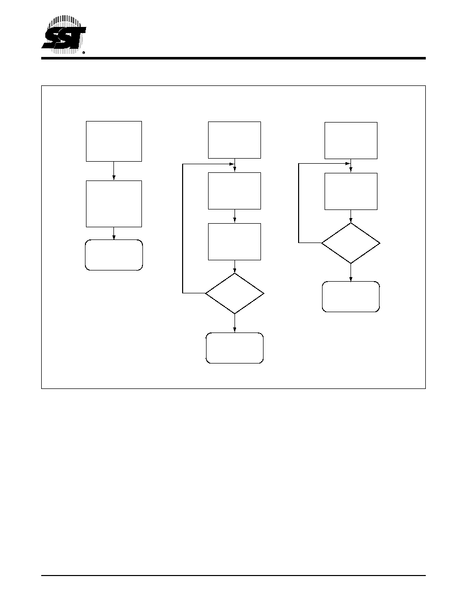
FIGURE 20: W
AIT
O
PTIONS
373 ILL F34.0
Wait TBP,
TSCE, TSE
or TBE
Program/Erase
Initiated
Internal Timer
Toggle Bit
Yes
Yes
No
No
Program/Erase
Completed
Does DQ6
match?
Read same
word
Data# Polling
Program/Erase
Completed
Program/Erase
Completed
Read word
Is DQ7 =
true data?
Read DQ7
Program/Erase
Initiated
Program/Erase
Initiated
Data Sheet
16 Mbit Concurrent SuperFlash
SST36VF1601
23
©2002 Silicon Storage Technology, Inc.
S71142-07-000
5/02
373
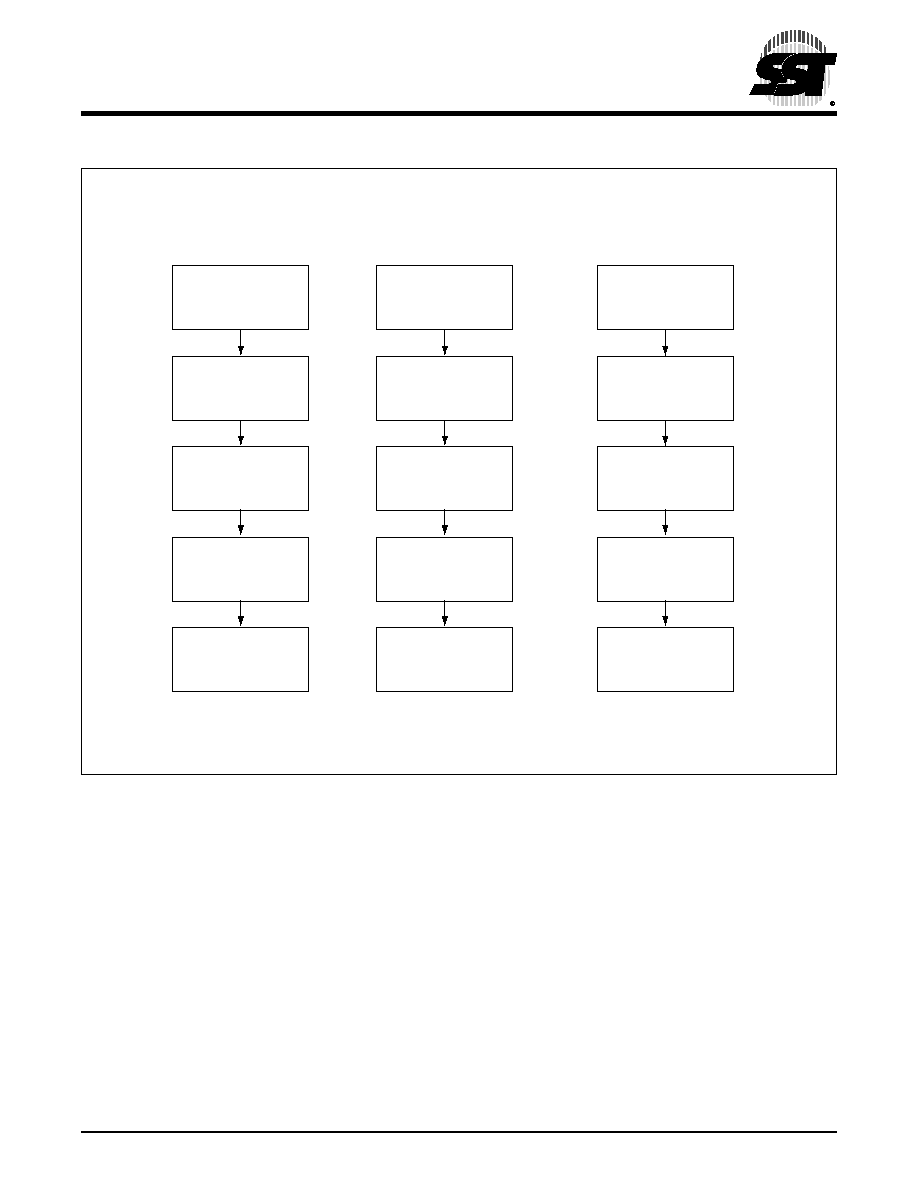
FIGURE 21: S
OFTWARE
P
RODUCT
ID/CFI C
OMMAND
F
LOWCHARTS
373 ILL F35.2
Load data: XXAAH
Address: 5555H
Software Product ID Entry
Command Sequence
Load data: XX55H
Address: 2AAAH
Load data: XX90H
Address: 5555H
Wait TIDA
Read Software ID
Load data: XXAAH
Address: 5555H
CFI Query Entry
Command Sequence
Load data: XX55H
Address: 2AAAH
Load data: XX98H
Address: 5555H
Wait TIDA
Read CFI data
Load data: XXAAH
Address: 5555H
Software ID Exit/CFI Exit
Command Sequence
Load data: XX55H
Address: 2AAAH
Load data: XXF0H
Address: 5555H
Wait TIDA
Return to normal
operation
Note: X can be VIL or VIH, but no other value.
24
Data Sheet
16 Mbit Concurrent SuperFlash
SST36VF1601
©2002 Silicon Storage Technology, Inc.
S71142-07-000
5/02
373
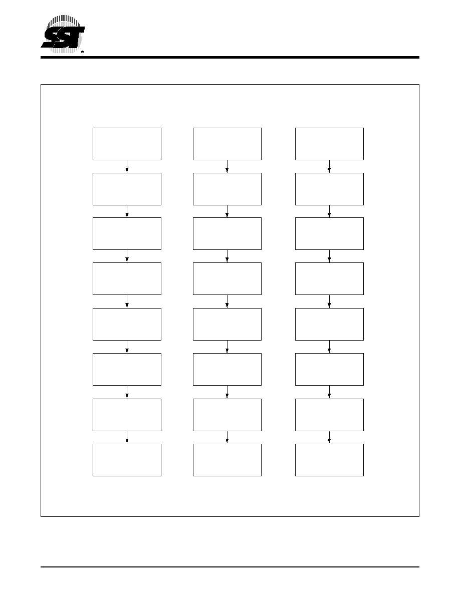
FIGURE 22: E
RASE
C
OMMAND
S
EQUENCE
373 ILL F36.2
Load data: XXAAH
Address: 5555H
Chip-Erase
Command Sequence
Load data: XX55H
Address: 2AAAH
Load data: XX80H
Address: 5555H
Load data: XX55H
Address: 2AAAH
Load data: XX10H
Address: 5555H
Load data: XXAAH
Address: 5555H
Wait TSCE
Chip erased
to FFFFH
Load data: XXAAH
Address: 5555H
Sector-Erase
Command Sequence
Load data: XX55H
Address: 2AAAH
Load data: XX80H
Address: 5555H
Load data: XX55H
Address: 2AAAH
Load data: XX30H
Address: SAX
Load data: XXAAH
Address: 5555H
Wait TSE
Sector erased
to FFFFH
Load data: XXAAH
Address: 5555H
Block-Erase
Command Sequence
Load data: XX55H
Address: 2AAAH
Load data: XX80H
Address: 5555H
Load data: XX55H
Address: 2AAAH
Load data: XX50H
Address: BAX
Load data: XXAAH
Address: 5555H
Wait TBE
Block erased
to FFFFH
Note: X can be VIL or VIH, but no other value.
Data Sheet
16 Mbit Concurrent SuperFlash
SST36VF1601
25
©2002 Silicon Storage Technology, Inc.
S71142-07-000
5/02
373
PRODUCT ORDERING INFORMATION
Valid combinations for SST36VF1601
SST36VF1601-70-4C-EK
SST36VF1601-70-4C-BK
SST36VF1601-70-4E-EK
SST36VF1601-70-4E-BK
Note:
Valid combinations are those products in mass production or will be in mass production. Consult your SST sales
representative to confirm availability of valid combinations and to determine availability of new combinations.
Device
Speed
Suffix1
Suffix2
SST36VF160 1 -
XXX
-
XX
-
XX
Package Modifier
K = 48 balls
Package Type
B = TFBGA (8mm x 10mm)
E = TSOP (type 1, die up, 12mm x 20mm)
Temperature Range
C = Commercial = 0∞C to +70∞C
E = Extended = -20∞C to +85∞C
Minimum Endurance
4 = 10,000 cycles
Read Access Speed
70 = 70 ns
Bank Split
1 = 12 Mbit + 4 Mbit
Device Density
160 = 1M x16
Voltage
V = 2.7-3.6V
26
Data Sheet
16 Mbit Concurrent SuperFlash
SST36VF1601
©2002 Silicon Storage Technology, Inc.
S71142-07-000
5/02
373
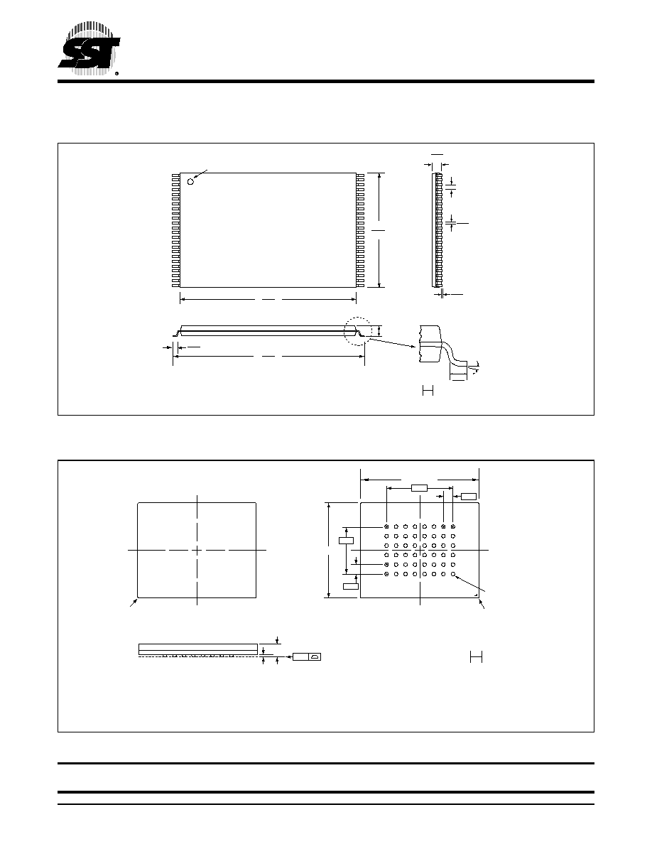
PACKAGING DIAGRAMS
48-
LEAD
T
HIN
S
MALL
O
UTLINE
P
ACKAGE
(TSOP) 12
MM
X
20
MM
SST P
ACKAGE
C
ODE
: EK
48-
BALL
T
HIN
-
PROFILE
, F
INE
-
PITCH
B
ALL
G
RID
A
RRAY
(TFBGA) 8
MM
X
10
MM
SST P
ACKAGE
C
ODE
: BK
1.05
0.95
0.70
0.50
18.50
18.30
20.20
19.80
0.70
0.50
12.20
11.80
0.27
0.17
0.15
0.05
48-tsop-EK-8
Note: 1. Complies with JEDEC publication 95 MO-142 DD dimensions,
although some dimensions may be more stringent.
2. All linear dimensions are in millimeters (max/min).
3. Coplanarity: 0.1 mm
4. Maximum allowable mold flash is 0.15 mm at the package ends, and 0.25 mm between leads.
1.20
max.
1mm
0∞- 5∞
DETAIL
Pin # 1 Identifier
0.50
BSC
A1 CORNER
H G F E D C B A
A B C D E F G H
BOTTOM VIEW
TOP VIEW
6
5
4
3
2
1
8.00 ± 0.20
0.30 ± 0.05
(48X)
A1 CORNER
10.00 ± 0.20
0.80
4.00
0.80
5.60
48-tfbga-BK-8x10-300mic-13
Note: 1. Although many dimensions are similar to those of JEDEC Publication 95, MO-210,
this specific package is not registered.
2. All linear dimensions are in millimeters.
3. Coplanarity: 0.08 mm
4. The actual shape of the corners may be slightly different than as portrayed in the drawing.
6
5
4
3
2
1
1mm
SIDE VIEW
SEATING PLANE
0.21 ± 0.05
1.10 ± 0.10
0.08
Silicon Storage Technology, Inc. ∑ 1171 Sonora Court ∑ Sunnyvale, CA 94086 ∑ Telephone 408-735-9110 ∑ Fax 408-735-9036
www.SuperFlash.com or www.sst.com