Data Sheet
©2001 Silicon Storage Technology, Inc.
S71146-03-000
6/01
396
1
The SST logo and SuperFlash are registered trademarks of Silicon Storage Technology, Inc.
MPF is a trademark of Silicon Storage Technology, Inc.
These specifications are subject to change without notice.
8 Mbit / 16 Mbit (x8) Multi-Purpose Flash
SST39LF080 / SST39LF016 / SST39VF080 / SST39VF016
FEATURES:
∑
Organized as 1M x8 / 2M x8
∑
Single Voltage Read and Write Operations
≠ 3.0-3.6V for SST39LF080/016
≠ 2.7-3.6V for SST39VF080/016
∑
Superior Reliability
≠ Endurance: 100,000 Cycles (typical)
≠ Greater than 100 years Data Retention
∑
Low Power Consumption:
≠ Active Current: 15 mA (typical)
≠ Standby Current: 4 µA (typical)
≠ Auto Low Power Mode: 4 µA (typical)
∑
Sector-Erase Capability
≠ Uniform 4 KByte sectors
∑
Block-Erase Capability
≠ Uniform 64 KByte blocks
∑
Fast Read Access Time:
≠ 55 ns for SST39LF080/016
≠ 70 and 90 ns for SST39VF080/016
∑
Latched Address and Data
∑
Fast Erase and Byte-Program:
≠ Sector-Erase Time: 18 ms (typical)
≠ Block-Erase Time: 18 ms (typical)
≠ Chip-Erase Time: 70 ms (typical)
≠ Byte-Program Time: 14 µs (typical)
≠ Chip Rewrite Time:
15 seconds (typical) for SST39LF/VF080
30 seconds (typical) for SST39LF/VF016
∑
Automatic Write Timing
≠ Internal V
PP
Generation
∑
End-of-Write Detection
≠ Toggle Bit
≠ Data# Polling
∑
CMOS I/O Compatibility
∑
JEDEC Standard
≠ Flash EEPROM Pinouts and command sets
∑
Packages Available
≠ 40-lead TSOP (10mm x 20mm)
≠ 48-ball TFBGA (6mm x 8mm)
PRODUCT DESCRIPTION
The SST39LF/VF080 and SST39LF/VF016 devices are
1M x8 / 2M x8 CMOS Multi-Purpose Flash (MPF) manu-
factured with SST's proprietary, high performance CMOS
SuperFlash technology. The split-gate cell design and thick
oxide tunneling injector attain better reliability and manufac-
turability compared with alternate approaches. The
SST39LF080/016 write (Program or Erase) with a 3.0-3.6V
power supply. The SST39VF080/016 write (Program or
Erase) with a 2.7-3.6V power supply. They conform to
JEDEC standard pinouts for x8 memories.
Featuring high performance Byte-Program, the SST39LF/
VF080 and SST39LF/VF016 devices provide a typical
Byte-Program time of 14 µsec. The devices use Toggle Bit
or Data# Polling to indicate the completion of Program
operation. To protect against inadvertent write, they have
on-chip hardware and Software Data Protection schemes.
Designed, manufactured, and tested for a wide spectrum of
applications, these devices are offered with a guaranteed
endurance of 10,000 cycles. Data retention is rated at
greater than 100 years.
The SST39LF/VF080 and SST39LF/VF016 devices are
suited for applications that require convenient and econom-
ical updating of program, configuration, or data memory.
For all system applications, they significantly improve per-
formance and reliability, while lowering power consumption.
They inherently use less energy during Erase and Program
than alternative flash technologies. The total energy con-
sumed is a function of the applied voltage, current, and
time of application. Since for any given voltage range, the
SuperFlash technology uses less current to program and
has a shorter erase time, the total energy consumed during
any Erase or Program operation is less than alternative
flash technologies. They also improve flexibility while lower-
ing the cost for program, data, and configuration storage
applications.
The SuperFlash technology provides fixed Erase and Pro-
gram times, independent of the number of Erase/Program
cycles that have occurred. Therefore the system software
or hardware does not have to be modified or de-rated as is
necessary with alternative flash technologies, whose Erase
and Program times increase with accumulated Erase/Pro-
gram cycles.
To meet high density, surface mount requirements, the
SST39LF/VF080 and SST39LF/VF016 are offered in 40-
lead TSOP and 48-ball TFBGA packaging. See Figures 1
and 2 for pinouts.
SST39LF/VF080 / 0163.0 & 2.7V 8Mb / 16Mb (x8) MPF memories
2
Data Sheet
8 Mbit / 16 Mbit Multi-Purpose Flash
SST39LF080 / SST39LF016 / SST39VF080 / SST39VF016
©2001 Silicon Storage Technology, Inc.
S71146-03-000
6/01
396
Device Operation
Commands are used to initiate the memory operation func-
tions of the device. Commands are written to the device
using standard microprocessor write sequences. A com-
mand is written by asserting WE# low while keeping CE#
low. The address bus is latched on the falling edge of WE#
or CE#, whichever occurs last. The data bus is latched on
the rising edge of WE# or CE#, whichever occurs first.
The SST39LF/VF080 and SST39LF/VF016 also have the
Auto Low Power mode which puts the device in a near
standby mode after data has been accessed with a valid
Read operation. This reduces the I
DD
active read current
from typically 15 mA to typically 4 µA. The Auto Low Power
mode reduces the typical I
DD
active read current to the
range of 1 mA/MHz of read cycle time. The device exits the
Auto Low Power mode with any address transition or con-
trol signal transition used to initiate another Read cycle,
with no access time penalty. Note that the device does not
enter Auto Low Power mode after power-up with CE# held
steadily low until the first address transition or CE# is driven
high.
Read
The Read operation of the SST39LF/VF080 and
SST39LF/VF016 is controlled by CE# and OE#, both have
to be low for the system to obtain data from the outputs.
CE# is used for device selection. When CE# is high, the
chip is deselected and only standby power is consumed.
OE# is the output control and is used to gate data from the
output pins. The data bus is in high impedance state when
either CE# or OE# is high. Refer to the Read cycle timing
diagram for further details (Figure 3).
Byte-Program Operation
The SST39LF/VF080 and SST39LF/VF016 are pro-
grammed on a byte-by-byte basis. Before programming,
one must ensure that the sector, in which the byte which is
being programmed exists, is fully erased. The Program
operation consists of three steps. The first step is the three-
byte load sequence for Software Data Protection. The sec-
ond step is to load byte address and byte data. During the
Byte-Program operation, the addresses are latched on the
falling edge of either CE# or WE#, whichever occurs last.
The data is latched on the rising edge of either CE# or
WE#, whichever occurs first. The third step is the internal
Program operation which is initiated after the rising edge of
the fourth WE# or CE#, whichever occurs first. The Pro-
gram operation, once initiated, will be completed within 20
µs. See Figures 4 and 5 for WE# and CE# controlled Pro-
gram operation timing diagrams and Figure 16 for flow-
charts. During the Program operation, the only valid reads
are Data# Polling and Toggle Bit. During the internal Pro-
gram operation, the host is free to perform additional tasks.
Any commands issued during the internal Program opera-
tion are ignored.
Sector/Block-Erase Operation
The Sector- (or Block-) Erase operation allows the system
to erase the device on a sector-by-sector (or block-by-
block) basis. The SST39LF/VF080 and SST39LF/VF016
offer both Sector-Erase and Block-Erase mode. The sector
architecture is based on uniform sector size of 4 KByte.
The Block-Erase mode is based on uniform block size of
64 KByte. The Sector-Erase operation is initiated by exe-
cuting a six-byte-command sequence with Sector-Erase
command (30H) and sector address (SA) in the last bus
cycle. The Block-Erase operation is initiated by executing a
six-byte-command sequence with Block-Erase command
(50H) and block address (BA) in the last bus cycle. The
sector or block address is latched on the falling edge of the
sixth WE# pulse, while the command (30H or 50H) is
latched on the rising edge of the sixth WE# pulse. The
internal Erase operation begins after the sixth WE# pulse.
The End-of-Erase operation can be determined using
either Data# Polling or Toggle Bit methods. See Figures 9
and 10 for timing waveforms. Any commands issued during
the Sector- or Block-Erase operation are ignored.
Chip-Erase Operation
The SST39LF/VF080 and SST39LF/VF016 provide a
Chip-Erase operation, which allows the user to erase the
entire memory array to the "1" state. This is useful when the
entire device must be quickly erased.
The Chip-Erase operation is initiated by executing a six
byte command sequence with Chip-Erase command (10H)
at address 5555H in the last byte sequence. The Erase
operation begins with the rising edge of the sixth WE# or
CE#, whichever occurs first. During the Erase operation,
the only valid read is Toggle Bit or Data# Polling. See Table
4 for the command sequence, Figure 8 for timing diagram,
and Figure 19 for the flowchart. Any commands issued dur-
ing the Chip-Erase operation are ignored.
Write Operation Status Detection
The SST39LF/VF080 and SST39LF/VF016 provide two
software means to detect the completion of a write (Pro-
gram or Erase) cycle, in order to optimize the system Write
cycle time. The software detection includes two status bits:
Data# Polling (DQ
7
) and Toggle Bit (DQ
6
). The End-of-Write
detection mode is enabled after the rising edge of WE#,
which initiates the internal Program or Erase operation.
Data Sheet
8 Mbit / 16 Mbit Multi-Purpose Flash
SST39LF080 / SST39LF016 / SST39VF080 / SST39VF016
3
©2001 Silicon Storage Technology, Inc.
S71146-03-000
6/01
396
The actual completion of the nonvolatile write is asynchro-
nous with the system; therefore, either a Data# Polling or
Toggle Bit read may be simultaneous with the completion
of the Write cycle. If this occurs, the system may possibly
get an erroneous result, i.e., valid data may appear to con-
flict with either DQ
7
or DQ
6
. In order to prevent spurious
rejection, if an erroneous result occurs, the software routine
should include a loop to read the accessed location an
additional two (2) times. If both reads are valid, then the
device has completed the Write cycle, otherwise the rejec-
tion is valid.
Data# Polling (DQ
7
)
When the SST39LF/VF080 and SST39LF/VF016 are in
the internal Program operation, any attempt to read DQ
7
will produce the complement of the true data. Once the
Program operation is completed, DQ
7
will produce true
data. The device is then ready for the next operation. Dur-
ing internal Erase operation, any attempt to read DQ
7
will
produce a `0'. Once the internal Erase operation is com-
pleted, DQ
7
will produce a `1'. The Data# Polling is valid
after the rising edge of fourth WE# (or CE#) pulse for Pro-
gram operation. For Sector-, Block- or Chip-Erase, the
Data# Polling is valid after the rising edge of sixth WE# (or
CE#) pulse. See Figure 6 for Data# Polling timing diagram
and Figure 17 for a flowchart.
Toggle Bit (DQ
6
)
During the internal Program or Erase operation, any con-
secutive attempts to read DQ
6
will produce alternating 1s
and 0s, i.e., toggling between 1 and 0. When the internal
Program or Erase operation is completed, the DQ
6
bit will
stop toggling. The device is then ready for the next opera-
tion. The Toggle Bit is valid after the rising edge of fourth
WE# (or CE#) pulse for Program operation. For Sector-,
Block-, or Chip-Erase, the Toggle Bit is valid after the rising
edge of sixth WE# (or CE#) pulse. See Figure 7 for Toggle
Bit timing diagram and Figure 17 for a flowchart.
Data Protection
The SST39LF/VF080 and SST39LF/VF016 provide both
hardware and software features to protect nonvolatile data
from inadvertent writes.
Hardware Data Protection
Noise/Glitch Protection: A WE# or CE# pulse of less than 5
ns will not initiate a Write cycle.
V
DD
Power Up/Down Detection: The Write operation is
inhibited when V
DD
is less than 1.5V.
Write Inhibit Mode: Forcing OE# low, CE# high, or WE#
high will inhibit the Write operation. This prevents inadvert-
ent writes during power-up or power-down.
Software Data Protection (SDP)
The SST39LF/VF080 and SST39LF/VF016 provide the
JEDEC approved Software Data Protection scheme for all
data alteration operations, i.e., Program and Erase. Any
Program operation requires the inclusion of the three-byte
sequence. The three-byte load sequence is used to initiate
the Program operation, providing optimal protection from
inadvertent Write operations, e.g., during the system
power-up or power-down. Any Erase operation requires the
inclusion of six-byte sequence. The SST39LF/VF080 and
SST39LF/VF016 devices are shipped with the Software
Data Protection permanently enabled. See Table 4 for the
specific software command codes. During SDP command
sequence, invalid commands will abort the device to read
mode within T
RC
.
Common Flash Memory Interface (CFI)
The SST39LF/VF080 and SST39LF/VF016 also contain
the CFI information to describe the characteristics of the
device. In order to enter the CFI Query mode, the system
must write three-byte sequence, same as product ID entry
command with 98H (CFI Query command) to address
5555H in the last byte sequence. Once the device enters
the CFI Query mode, the system can read CFI data at the
addresses given in Tables 5 through 8. The system must
write the CFI Exit command to return to Read mode from
the CFI Query mode.
4
Data Sheet
8 Mbit / 16 Mbit Multi-Purpose Flash
SST39LF080 / SST39LF016 / SST39VF080 / SST39VF016
©2001 Silicon Storage Technology, Inc.
S71146-03-000
6/01
396
Product Identification
The Product Identification mode identifies the device as the
SST39LF080, SST39VF080, SST39LF016, and
SST39VF016 and manufacturer as SST. This mode may
be accessed by software operations. Users may use the
Software Product Identification operation to identify the part
(i.e., using the device ID) when using multiple manufactur-
ers in the same socket. For details, see Table 4 for software
operation, Figure 11 for the Software ID Entry and Read
timing diagram and Figure 18 for the Software ID Entry
command sequence flowchart.
Product Identification Mode Exit/
CFI Mode Exit
In order to return to the standard Read mode, the Software
Product Identification mode must be exited. Exit is accom-
plished by issuing the Software ID Exit command
sequence, which returns the device to the Read operation.
This command may also be used to reset the device to the
Read mode after any inadvertent transient condition that
apparently causes the device to behave abnormally, e.g.,
not read correctly. Please note that the Software ID Exit/
CFI Exit command is ignored during an internal Program or
Erase operation. See Table 4 for software command
codes, Figure 13 for timing waveform and Figure 18 for a
flowchart.
TABLE
1: P
RODUCT
I
DENTIFICATION
Address
Data
Manufacturer's ID
0000H
BFH
Device ID
SST39LF/VF080
0001H
D8H
SST39LF/VF016
0001H
D9H
T1.2 396
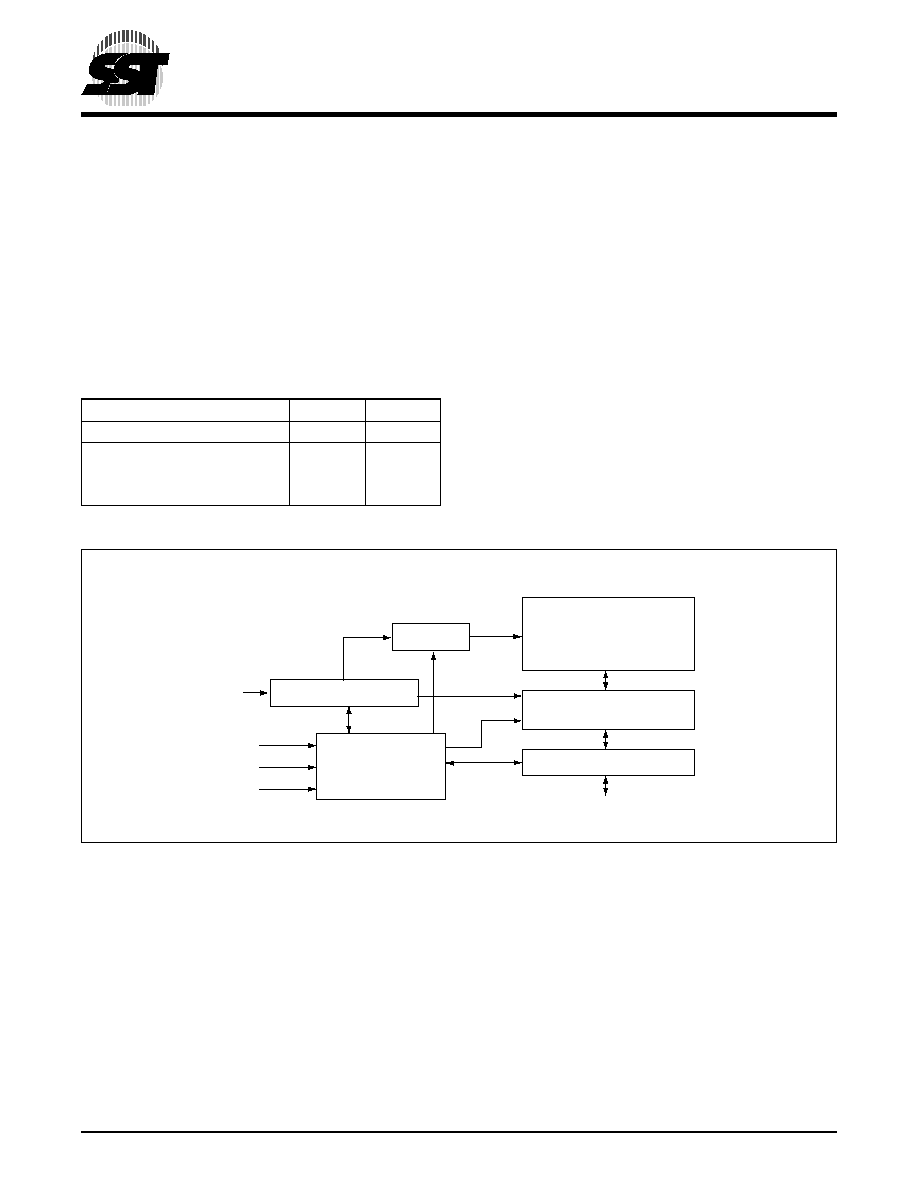
Y-Decoder
I/O Buffers and Data Latches
396 ILL B1.2
Address Buffer & Latches
X-Decoder
DQ7 - DQ0
Memory
Address
OE#
CE#
WE#
SuperFlash
Memory
Control Logic
F
UNCTIONAL
B
LOCK
D
IAGRAM
Data Sheet
8 Mbit / 16 Mbit Multi-Purpose Flash
SST39LF080 / SST39LF016 / SST39VF080 / SST39VF016
5
©2001 Silicon Storage Technology, Inc.
S71146-03-000
6/01
396
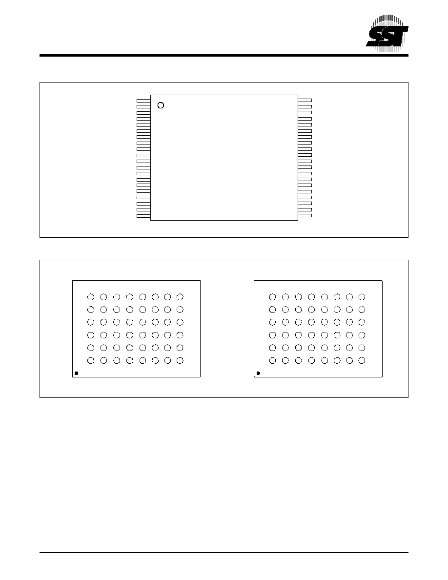
FIGURE 1: P
IN
A
SSIGNMENTS
FOR
40-
LEAD
TSOP
FIGURE 2: P
IN
A
SSIGNMENTS
FOR
48-
BALL
TFBGA
SST39LF/VF080 SST39LF/VF016
A16
A15
A14
A13
A12
A11
A9
A8
WE#
NC
NC
NC
A18
A7
A6
A5
A4
A3
A2
A1
A16
A15
A14
A13
A12
A11
A9
A8
WE#
NC
NC
NC
A18
A7
A6
A5
A4
A3
A2
A1
1
2
3
4
5
6
7
8
9
10
11
12
13
14
15
16
17
18
19
20
A17
VSS
NC
A19
A10
DQ7
DQ6
DQ5
DQ4
VDD
VDD
NC
DQ3
DQ2
DQ1
DQ0
OE#
VSS
CE#
A0
40
39
38
37
36
35
34
33
32
31
30
29
28
27
26
25
24
23
22
21
396 ILL F01.2
Standard Pinout
Top View
Die Up
SST39LF/VF160 SST39LF/VF080
A17
VSS
A20
A19
A10
DQ7
DQ6
DQ5
DQ4
VDD
VDD
NC
DQ3
DQ2
DQ1
DQ0
OE#
VSS
CE#
A0
A14
A9
WE#
NC
A7
A3
A13
A8
NC
NC
A18
A4
A15
A11
NC
NC
A6
A2
A16
A12
NC
NC
A5
A1
A17
A19
DQ5
DQ2
DQ0
A0
NC
A10
NC
DQ3
NC
CE#
A20
DQ6
VDD
VDD
NC
OE#
VSS
DQ7
DQ4
NC
DQ1
VSS
396 ILL F21.1
SST39LF/VF016
TOP VIEW (balls facing down)
6
5
4
3
2
1
A B C D E F G H
A14
A9
WE#
NC
A7
A3
A13
A8
NC
NC
A18
A4
A15
A11
NC
NC
A6
A2
A16
A12
NC
NC
A5
A1
A17
A19
DQ5
DQ2
DQ0
A0
NC
A10
NC
DQ3
NC
CE#
NC
DQ6
VDD
VDD
NC
OE#
VSS
DQ7
DQ4
NC
DQ1
VSS
396 ILL F20.1
SST39LF/VF080
TOP VIEW (balls facing down)
6
5
4
3
2
1
A B C D E F G H