
©2001 Silicon Storage Technology, Inc.
S71161-06-000
9/01
504
1
The SST logo and SuperFlash are registered trademarks of Silicon Storage Technology, Inc.
MPF is a trademark of Silicon Storage Technology, Inc. Intel is a registered trademark of Intel Corporation.
These specifications are subject to change without notice.
Advance Information
FEATURES:
∑
Firmware Hub for Intel 8xx Chipsets
∑
2 Mbit, 3 Mbit, 4 Mbit, or 8 Mbit SuperFlash
memory array for code/data storage
≠ SST49LF002A: 256K x8 (2 Mbit)
≠ SST49LF003A: 384K x8 (3 Mbit)
≠ SST49LF004A: 512K x8 (4 Mbit)
≠ SST49LF008A: 1024K x8 (8 Mbit)
∑
Flexible Erase Capability
≠ Uniform 4 KByte Sectors
≠ Uniform 16 KByte overlay blocks for
SST49LF002A
≠ Uniform 64 KByte overlay blocks for
SST49LF003A/004A/008A
≠ Top Boot Block protection
- 16 KByte for SST49LF002A
- 64 KByte for SST49LF003A/004A/008A
≠ Chip-Erase for PP Mode Only
∑
Single 3.0-3.6V Read and Write Operations
∑
Superior Reliability
≠ Endurance:100,000 Cycles (typical)
≠ Greater than 100 years Data Retention
∑
Low Power Consumption
≠ Active Read Current: 6 mA (typical)
≠ Standby Current: 10 µA (typical)
∑
Fast Sector-Erase/Byte-Program Operation
≠ Sector-Erase Time: 18 ms (typical)
≠ Block-Erase Time: 18 ms (typical)
≠ Chip-Erase Time: 70 ms (typical)
≠ Byte-Program Time: 14 µs (typical)
≠ Chip Rewrite Time:
SST49LF002A: 4 seconds (typical)
SST49LF003A: 6 seconds (typical)
SST49LF004A: 8 seconds (typical)
SST49LF008A: 15 seconds (typical)
≠ Single-pulse Program or Erase
≠ Internal timing generation
∑
Two Operational Modes
≠ Firmware Hub Interface (FWH) Mode for
in-system operation
≠ Parallel Programming (PP) Mode for fast
production programming
∑
Firmware Hub Hardware Interface Mode
≠ 5-signal communication interface supporting
byte Read and Write
≠ 33 MHz clock frequency operation
≠ WP# and TBL# pins provide hardware write
protect for entire chip and/or top Boot Block
≠ Block Locking Register for all blocks
≠ Standard SDP Command Set
≠ Data# Polling and Toggle Bit for End-of-Write
detection
≠ 5 GPI pins for system design flexibility
≠ 4 ID pins for multi-chip selection
∑
Parallel Programming (PP) Mode
≠ 11-pin multiplexed address and
8-pin data I/O interface
≠ Supports fast In-System or PROM programming
for manufacturing
∑
CMOS and PCI I/O Compatibility
∑
Packages Available
≠ 32-lead PLCC
≠ 32-lead TSOP (8mm x 14mm)
PRODUCT DESCRIPTION
The SST49LF00xA flash memory devices are designed
to be read-compatible with the Intel 82802 Firmware Hub
(FWH) device for PC-BIOS application. It provides pro-
tection for the storage and update of code and data in
addition to adding system design flexibility through five
general purpose inputs. Two interface modes are sup-
ported by the SST49LF00xA: Firmware Hub (FWH)
Interface Mode for In-System programming and Parallel
Programming (PP) Mode for fast factory programming of
PC-BIOS applications.
The SST49LF00xA flash memory devices are manufac-
tured with SST's proprietary, high performance Super-
Flash Technology. The split-gate cell design and thick
oxide tunneling injector attain better reliability and manu-
facturability compared with alternate approaches. The
SST49LF00xA devices significantly improve performance
and reliability, while lowering power consumption. The
SST49LF00xA devices write (Program or Erase) with a
single 3.0-3.6V power supply. It uses less energy during
Erase and Program than alternative flash memory tech-
nologies. The total energy consumed is a function of the
applied voltage, current and time of application. Since for
2 Mbit / 3 Mbit / 4 Mbit / 8 Mbit Firmware Hub
SST49LF002A / SST49LF003A / SST49LF004A / SST49LF008A
SST49LF002A / 003A / 004A / 008A2 Mb / 3 Mb / 4 Mb / 8 Mb Firmware Hub for Intel 8xx Chipsets

2
Advance Information
2 Mbit / 3 Mbit / 4 Mbit / 8 Mbit Firmware Hub
SST49LF002A / SST49LF003A / SST49LF004A / SST49LF008A
©2001 Silicon Storage Technology, Inc.
S71161-06-000
9/01
504
any given voltage range, the SuperFlash technology uses
less current to program and has a shorter erase time, the
total energy consumed during any Erase or Program oper-
ation is less than alternative flash memory technologies.
The SST49LF00xA products provide a maximum Byte-
Program time of 20 µsec. The entire memory can be
erased and programmed byte-by-byte typically in 15 sec-
onds for an 8-Mbit device, when using status detection
features such as Toggle Bit or Data# Polling to indicate the
completion of Program operation. The SuperFlash tech-
nology provides fixed Erase and Program time, indepen-
dent of the number of Erase/Program cycles that have
performed. Therefore the system software or hardware
does not have to be calibrated or correlated to the cumu-
lated number of Erase/Program cycles as is necessary
with alternative flash memory technologies, whose Erase
and Program time increase with accumulated Erase/Pro-
gram cycles.
To protect against inadvertent write, the SST49LF00xA
devices employ hardware and software data (SDP) protec-
tion schemes. It is offered with typical endurance of
100,000 cycles. Data retention is rated at greater than 100
years.
To meet high density, surface mount requirements, the
SST49LF00xA device is offered in 32-lead TSOP and 32-
lead PLCC packages. See Figures 7 and 8 for pinouts and
Table 8 for pin descriptions.
Mode Selection and Description
The SST49LF00xA flash memory devices can operate in
two distinct interface modes: the Firmware Hub Interface
(FWH) mode and the Parallel Programming (PP) mode.
The IC (Interface Configuration pin) is used to set the
interface mode selection. If the IC pin is set to logic High,
the device is in PP mode; while if the IC pin is set Low,
the device is in the FWH mode. The IC selection pin must
be configured prior to device operation. The IC pin is
internally pulled down if the pin is not connected. In FWH
mode, the device is configured to interface with its host
using Intel's Firmware Hub proprietary protocol. Commu-
nication between Host and the SST49LF00xA occurs via
the 4-bit I/O communication signals, FWH [3:0] and the
FWH4. In PP mode, the device is programmed via an 11-
bit address and an 8-bit data I/O parallel signals. The
address inputs are multiplexed in row and column
selected by control signal R/C# pin. The column
addresses are mapped to the higher internal addresses,
and the row addresses are mapped to the lower internal
addresses. See the Device Memory Maps in Figures 3
through 6 for address assignments.
FIRMWARE HUB (FWH) MODE
Device Operation
The FWH mode uses a 5-signal communication interface,
FWH[3:0] and FWH4, to control operations of the
SST49LF00xA. Operations such as Memory Read and
Memory Write uses Intel FWH propriety protocol. JEDEC
Standard SDP (Software Data Protection) Byte-Program,
Sector-Erase and Block-Erase command sequences are
incorporated into the FWH memory cycles. Chip-Erase is
only available in PP Mode.
The device enters standby mode when FWH4 is high and
no internal operation is in progress. The device is in ready
mode when FWH4 is low and no activity is on the FWH bus.
Firmware Hub Interface Cycles
Addresses and data are transferred to and from the
SST49LF00xA by a series of "fields," where each field con-
tains 4 bits of data. ST49LF00xA supports only single-byte
read and writes, and all fields are one clock cycle in length.
Field sequences and contents are strictly defined for Read
and Write operations. Addresses in this section refer to
addresses as seen from the SST49LF00xA's "point of
view," some calculation will be required to translate these to
the actual locations in the memory map (and vice versa) if
multiple memory device is used on the bus. Tables 1 and 2
list the field sequences for Read and Write cycles.
Advance Information
2 Mbit / 3 Mbit / 4 Mbit / 8 Mbit Firmware Hub
SST49LF002A / SST49LF003A / SST49LF004A / SST49LF008A
3
©2001 Silicon Storage Technology, Inc.
S71161-06-000
9/01
504
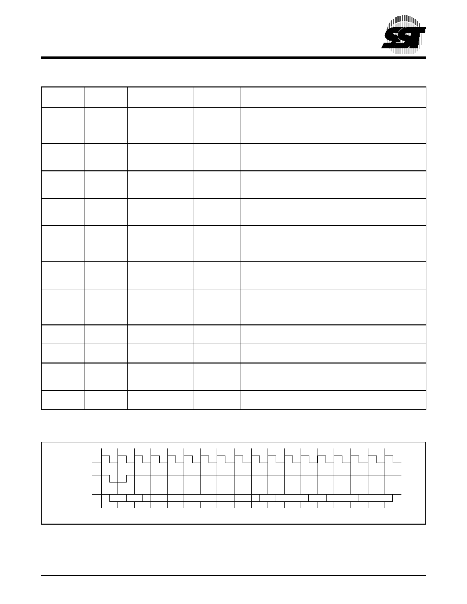
FIGURE 1: S
INGLE
-B
YTE
R
EAD
W
AVEFORMS
TABLE
1: FWH R
EAD
C
YCLE
Clock
Cycle
Field
Name
Field Contents
FWH[3:0]
1
FWH[3:0]
Direction
Comments
1
START
1101
IN
FWH4 must be active (low) for the part to respond. Only the
last start field (before FWH4 transitioning high) should be
recognized. The START field contents indicate a FWH
memory read cycle.
2
IDSEL
0000 to 1111
IN
Indicates which FWH device should respond. If the to IDSEL (ID
select) field matches the value ID[3:0], then that particular device
will respond to the whole bus cycle.
3-9
IMADDR
YYYY
IN
These seven clock cycles make up the 28-bit memory
address. YYYY is one nibble of the entire address.
Addresses are transferred most-significant nibble first.
10
IMSIZE
0000 (1 byte)
IN
A field of this size indicates how many bytes will be or trans-
ferred during multi-byte operations. The SST49LF00xA will
only support single-byte operation. IMSIZE=0000b
11
TAR0
1111
IN
then Float
In this clock cycle, the master (Intel ICH) has driven the bus
then float to all `1's and then floats the bus, prior to the next
clock cycle. This is the first part of the bus "turnaround
cycle."
12
TAR1
1111 (float)
Float
then OUT
The SST49LF00xA takes control of the bus during this
cycle. During the next clock cycle, it will be driving "sync
data."
13
RSYNC
0000 (READY)
OUT
During this clock cycle, the FWH will generate a "ready-
sync" (RSYNC) indicating that the least-significant nibble of
the least-significant byte will be available during the next
clock cycle.
14
DATA
YYYY
OUT
YYYY is the least-significant nibble of the least-significant
data byte.
15
DATA
YYYY
OUT
YYYY is the most-significant nibble of the least-significant
data byte.
16
TAR0
1111
OUT
then Float
In this clock cycle, the SST49LF00xA has driven the bus to
all ones and then floats the bus prior to the next clock cycle.
This is the first part of the bus "turnaround cycle."
17
TAR1
1111 (float)
Float then
IN
The master (Intel ICH) resumes control of the bus during
this cycle.
T1.3 504
1. Field contents are valid on the rising edge of the present clock cycle.
CLK
FWH4
FWH[3:0]
504 ILL F59.1
STR
TAR
RSYNC
IMS
IMADDR
IDS
DATA
TAR
4
Advance Information
2 Mbit / 3 Mbit / 4 Mbit / 8 Mbit Firmware Hub
SST49LF002A / SST49LF003A / SST49LF004A / SST49LF008A
©2001 Silicon Storage Technology, Inc.
S71161-06-000
9/01
504
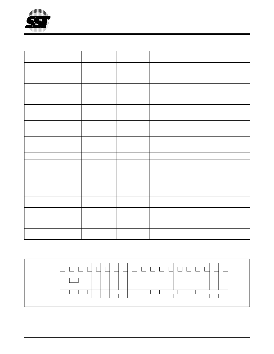
FIGURE 2: W
RITE
W
AVEFORMS
TABLE
2: FWH W
RITE
C
YCLE
Clock
Cycle
Field
Name
Field Contents
FWH[3:0]
1
FWH[3:0]
Direction
Comments
1
START
1110
IN
FWH4 must be active (low) for the part to respond.
Only the last start field (before FWH4 transitioning
high) should be recognized. The START field contents
indicate a FWH memory read cycle.
2
IDSEL
0000 to 1111
IN
Indicates which SST49LF00xA device should
respond. If the IDSEL (ID select) field matches the
value ID[3:0], then that particular device will respond
to the whole bus cycle.
3-9
IMADDR
YYYY
IN
These seven clock cycles make up the 28-bit memory
address. YYYY is one nibble of the entire address.
Addresses are transferred most-significant nibble first.
10
IMSIZE
0000 (1 byte)
IN
This size field indicates how many bytes will be
transferred during multi-byte operations. The FWH
only supports single-byte writes. IMSIZE=0000b
11
DATA
YYYY
IN
This field is the least-significant nibble of the data byte.
This data is either the data to be programmed into the
flash memory or any valid flash command.
12
DATA
YYYY
IN
This field is the most-significant nibble of the data byte.
13
TAR0
1111
IN then Float
In this clock cycle, the master (Intel ICH) has driven the
then float bus to all `1's and then floats the bus prior to
the next clock cycle. This is the first part of the bus
"turnaround cycle."
14
TAR1
1111 (float)
Float then OUT
The SST49LF00xA takes control of the bus during this
cycle. During the next clock cycle it will be driving the
"sync" data.
15
RSYNC
0000
OUT
The SST49LF00xA outputs the values 0000, indicat-
ing that it has received data or a flash command.
16
TAR0
1111
OUT then Float
In this clock cycle, the SST49LF00xA has driven the
bus to all then float `1's and then floats the bus prior to
the next clock cycle. This is the first part of the bus
"turnaround cycle."
17
TAR1
1111 (float)
Float then IN
The master (Intel ICH) resumes control of the bus during
this cycle.
T2.4 504
1. Field contents are valid on the rising edge of the present clock cycle.
CLK
FWH4
FWH[3:0]
504 ILL F60.1
STR
DATA
TAR
TAR
RSYNC
IMS
IMADDR
IDS

Advance Information
2 Mbit / 3 Mbit / 4 Mbit / 8 Mbit Firmware Hub
SST49LF002A / SST49LF003A / SST49LF004A / SST49LF008A
5
©2001 Silicon Storage Technology, Inc.
S71161-06-000
9/01
504
Abort Mechanism
If FWH4 is driven low for one or more clock cycles during a
FWH cycle, the cycle will be terminated and the device will
wait for the ABORT command. The host must drive the
FWH[3:0] with `1111b' (ABORT command) to return the
device to ready mode. If abort occurs during the internal
write cycle, the data may be incorrectly programmed or
erased. It is required to wait for the Write operation to com-
plete prior to initiation of the abort command. It is recom-
mended to check the Write status with Data# Polling (DQ
7
)
or Toggle Bit (DQ
6
) pins. One other option is to wait for the
fixed write time to expire.
Response To Invalid Fields
During FWH operations, the FWH will not explicitly indicate
that it has received invalid field sequences. The response
to specific invalid fields or sequences is as follows:
Address out of range: The FWH address sequence is
7 fields long (28 bits), but only the last five address fields
(20 bits) will be decoded by SST49LF00xA.
Address A
22
has the special function of directing reads and
writes to the flash core (A
22
=1) or to the register space
(A
22
=0).
The SST49LF003A features are equivalent to the
SST49LF004A with 128 KByte less memory. For the
SST49LF003A, operations beyond the 3-Mbit bound-
ary (below 20000H) are not valid (see Device Memory
Map). Invalid address range locations will read as
00H.
Invalid IMSIZE field: If the FWH receives an invalid size
field during a Read or Write operation, the device will reset
and no operation will be attempted. The SST49LF00xA will
not generate any kind of response in this situation. Invalid-
size fields for a Read/Write cycle are anything but 0000b.
Once valid START, IDSEL, and IMSIZE fields are received,
the SST49LF00xA always will respond to subsequent
inputs as if they were valid. As long as the states of device
FWH[3:0] and FWH4 are known, the response of the
SST49LF00xA to signals received during the FWH cycle
should be predictable. The SST49LF00xA will make no
attempt to check the validity of incoming flash operation
commands.
Device Memory Hardware Write Protection
The Top Boot Lock (TBL#) and Write Protect (WP#) pins
are provided for hardware write protection of device
memory in the SST49LF00xA. The TBL# pin is used to
write protect 16 boot sectors (64 KByte) at the highest
flash memory address range for the SST49LF003A/
004A/008A and 4 boot sectors (16 KByte) for
SST49LF002A. WP# pin write protects the remaining
sectors in the flash memory.
An active low signal at the TBL# pin prevents Program and
Erase operations of the top boot sectors. When TBL# pin is
held high, write protection of the top boot sectors is then
determined by the Boot Block Locking register. The WP#
pin serves the same function for the remaining sectors of
the device memory. The TBL# and WP# pins write protec-
tion functions operate independently of one another.
Both TBL# and WP# pins must be set to their required
protection states prior to starting a Program or Erase
operation. A logic level change occurring at the TBL# or
WP# pin during a Program or Erase operation could
cause unpredictable results. TBL# and WP# pins cannot
be left unconnected.
TBL# is internally ORed with the top Boot Block Locking
register. When TBL# is low, the top Boot Block is hard-
ware write protected regardless of the state of the Write-
Lock bit for the Boot Block Locking register. Clearing the
Write-Protect bit in the register when TBL# is low will have
no functional effect, even though the register may indicate
that the block is no longer locked.
WP# is internally ORed with the Block Locking register.
When WP# is low, the blocks are hardware write pro-
tected regardless of the state of the Write-Lock bit for the
corresponding Block Locking registers. Clearing the
Write-Protect bit in any register when WP# is low will have
no functional effect, even though the register may indicate
that the block is no longer locked.
Reset
A V
IL
on INIT# or RST# pin initiates a device reset. INIT#
and RST# pins have the same function internally. It is
required to drive INIT# or RST# pins low during a system
reset to ensure proper CPU initialization.
During a Read operation, driving INIT# or RST# pins low
deselects the device and places the output drivers,
FWH[3:0], in a high-impedance state. The reset signal
must be held low for a minimal duration of time T
RSTP.
A
reset latency will occur if a reset procedure is performed
during a Program or Erase operation. See Table 18, Reset
Timing Parameters for more information. A device reset
during an active Program or Erase will abort the operation
and memory contents may become invalid due to data
being altered or corrupted from an incomplete Erase or
Program operation.