
©2004 Silicon Storage Technology, Inc.
S71255-00-000
3/04
1
The SST logo, SuperFlash, and FlashFlex are registered trademarks of Silicon Storage Technology, Inc.
These specifications are subject to change without notice.
Preliminary Specifications
FEATURES:
∑
8-bit 8051-Compatible Microcontroller (MCU)
with Embedded SuperFlash Memory
≠ Fully Software Compatible
≠ Development Toolset Compatible
≠ Pin-For-Pin Package Compatible
∑
SST89E5xxRD2 Operation
≠ 0 to 40 MHz at 5V
∑
SST89V5xxRD2 Operation
≠ 0 to 33 MHz at 3V
∑
1 KByte Internal RAM
∑
Dual Block SuperFlash EEPROM
≠ 8/16/32/64 KByte primary block +
8 KByte secondary block
(128-Byte sector size for both blocks)
≠ Individual Block Security Lock with SoftLock
≠ Concurrent Operation during
In-Application Programming (IAP)
≠ Memory Overlay for Interrupt Support during IAP
∑
Support External Address Range up to 64
KByte of Program and Data Memory
∑
Three High-Current Drive Ports (16 mA each)
∑
Three 16-bit Timers/Counters
∑
Full-Duplex, Enhanced UART
≠ Framing Error Detection
≠ Automatic Address Recognition
∑
Ten Interrupt Sources at 4 Priority Levels
≠ Four External Interrupt Inputs
∑
Programmable Watchdog Timer (WDT)
∑
Programmable Counter Array (PCA)
∑
Four 8-bit I/O Ports (32 I/O Pins) and
One 4-bit Port
∑
Second DPTR register
∑
Low EMI Mode (Inhibit ALE)
∑
SPI Serial Interface
∑
Standard 12 Clocks per cycle, the device has an
option to double the speed to 6 clocks per cycle.
∑
TTL- and CMOS-Compatible Logic Levels
∑
Brown-out Detection
∑
Low Power Modes
≠ Power-down Mode with External Interrupt Wake-up
≠ Idle Mode
∑
Temperature Ranges:
≠ Commercial (0∞C to +70∞C)
≠ Industrial (-40∞C to +85∞C)
∑
Packages Available
≠ 44-lead PLCC
≠ 40-pin PDIP (Port 4 feature not available)
≠ 44-lead TQFP
PRODUCT DESCRIPTION
The SST89E5xxRD2 and SST89V5xxRD2 are members
of the FlashFlex51 family of 8-bit microcontroller products
designed and manufactured with SST's patented and pro-
prietary SuperFlash CMOS semiconductor process tech-
nology. The split-gate cell design and thick-oxide tunneling
injector offer significant cost and reliability benefits for SST's
customers. The devices use the 8051 instruction set and
are pin-for-pin compatible with standard 8051 microcontrol-
ler devices.
The devices come with 16/24/40/72 KByte of on-chip flash
EEPROM program memory which is partitioned into 2
independent program memory blocks. The primary Block 0
occupies 8/16/32/64 KByte of internal program memory
space and the secondary Block 1 occupies 8 KByte of
internal program memory space.
The 8-KByte secondary block can be mapped to the lowest
location of the 8/16/32/64 KByte address space; it can also
be hidden from the program counter and used as an inde-
pendent EEPROM-like data memory.
In addition to the 16/24/40/72 KByte of EEPROM program
memory on-chip, the devices can address up to 64 KByte
of external program memory. In addition to 1024 x8 bits of
on-chip RAM, up to 64 KByte of external RAM can be
addressed.
The flash memory blocks can be programmed via a stan-
dard 87C5x OTP EPROM programmer fitted with a special
adapter and the firmware for SST's devices. During power-
on reset, the devices can be configured as either a slave to
an external host for source code storage or a master to an
external host for an in-application programming (IAP) oper-
ation. The devices are designed to be programmed in-sys-
tem and in-application on the printed circuit board for
maximum flexibility. The devices are pre-programmed with
an example of the bootstrap loader in the memory, demon-
strating the initial user program code loading or subsequent
user code updating via the IAP operation. The sample
bootstrap loader is available for the user's reference and
convenience only; SST does not guarantee its functionality
or usefulness. Chip-Erase or Block-Erase operations will
erase the pre-programmed sample code.
FlashFlex51 MCU
SST89E52RD2 / SST89E54RD2 / SST89E58RD2 / SST89E516RD2
SST89V52RD2 / SST89V54RD2 / SST89V58RD2 / SST89V516RD2
SST89E/V516 / 58 / 54 / 52RD2 FlashFlex51 MCU

2
Preliminary Specifications
FlashFlex51 MCU
SST89E52RD2 / SST89E54RD2 / SST89E58RD2 / SST89E516RD2
SST89V52RD2 / SST89V54RD2 / SST89V58RD2 / SST89V516RD2
©2004 Silicon Storage Technology, Inc.
S71255-00-000
3/04
TABLE OF CONTENTS
PRODUCT DESCRIPTION . . . . . . . . . . . . . . . . . . . . . . . . . . . . . . . . . . . . . . . . . . . . . . . . . . . . . . . . . . . . . . . . . . . 1
LIST OF FIGURES . . . . . . . . . . . . . . . . . . . . . . . . . . . . . . . . . . . . . . . . . . . . . . . . . . . . . . . . . . . . . . . . . . . . . . . . . 4
LIST OF TABLES. . . . . . . . . . . . . . . . . . . . . . . . . . . . . . . . . . . . . . . . . . . . . . . . . . . . . . . . . . . . . . . . . . . . . . . . . . . 5
1.0 FUNCTIONAL BLOCKS . . . . . . . . . . . . . . . . . . . . . . . . . . . . . . . . . . . . . . . . . . . . . . . . . . . . . . . . . . . . . . . . . 7
2.0 PIN ASSIGNMENTS. . . . . . . . . . . . . . . . . . . . . . . . . . . . . . . . . . . . . . . . . . . . . . . . . . . . . . . . . . . . . . . . . . . . 8
2.1 Pin Descriptions . . . . . . . . . . . . . . . . . . . . . . . . . . . . . . . . . . . . . . . . . . . . . . . . . . . . . . . . . . . . . . . . . . . . 9
3.0 MEMORY ORGANIZATION . . . . . . . . . . . . . . . . . . . . . . . . . . . . . . . . . . . . . . . . . . . . . . . . . . . . . . . . . . . . . 11
3.1 Program Flash Memory . . . . . . . . . . . . . . . . . . . . . . . . . . . . . . . . . . . . . . . . . . . . . . . . . . . . . . . . . . . . . 11
3.2 Program Memory Block Switching . . . . . . . . . . . . . . . . . . . . . . . . . . . . . . . . . . . . . . . . . . . . . . . . . . . . . 13
3.3 Data RAM Memory. . . . . . . . . . . . . . . . . . . . . . . . . . . . . . . . . . . . . . . . . . . . . . . . . . . . . . . . . . . . . . . . . 14
3.4 Expanded Data RAM Addressing . . . . . . . . . . . . . . . . . . . . . . . . . . . . . . . . . . . . . . . . . . . . . . . . . . . . . 14
3.5 Dual Data Pointers . . . . . . . . . . . . . . . . . . . . . . . . . . . . . . . . . . . . . . . . . . . . . . . . . . . . . . . . . . . . . . . . . 17
3.6 Special Function Registers . . . . . . . . . . . . . . . . . . . . . . . . . . . . . . . . . . . . . . . . . . . . . . . . . . . . . . . . . . 17
4.0 FLASH MEMORY PROGRAMMING . . . . . . . . . . . . . . . . . . . . . . . . . . . . . . . . . . . . . . . . . . . . . . . . . . . . . . 35
4.1 External Host Programming Mode . . . . . . . . . . . . . . . . . . . . . . . . . . . . . . . . . . . . . . . . . . . . . . . . . . . . . 35
4.2 In-Application Programming Mode. . . . . . . . . . . . . . . . . . . . . . . . . . . . . . . . . . . . . . . . . . . . . . . . . . . . . 39
5.0 TIMERS/COUNTERS . . . . . . . . . . . . . . . . . . . . . . . . . . . . . . . . . . . . . . . . . . . . . . . . . . . . . . . . . . . . . . . . . . 44
5.1 Timers . . . . . . . . . . . . . . . . . . . . . . . . . . . . . . . . . . . . . . . . . . . . . . . . . . . . . . . . . . . . . . . . . . . . . . . . . . 44
5.2 Timer Set-up . . . . . . . . . . . . . . . . . . . . . . . . . . . . . . . . . . . . . . . . . . . . . . . . . . . . . . . . . . . . . . . . . . . . . 44
5.3 Programmable Clock-Out. . . . . . . . . . . . . . . . . . . . . . . . . . . . . . . . . . . . . . . . . . . . . . . . . . . . . . . . . . . . 45
6.0 SERIAL I/O . . . . . . . . . . . . . . . . . . . . . . . . . . . . . . . . . . . . . . . . . . . . . . . . . . . . . . . . . . . . . . . . . . . . . . . . . . 45
6.1 Full-Duplex, Enhanced UART . . . . . . . . . . . . . . . . . . . . . . . . . . . . . . . . . . . . . . . . . . . . . . . . . . . . . . . . 45
6.2 Serial Peripheral Interface . . . . . . . . . . . . . . . . . . . . . . . . . . . . . . . . . . . . . . . . . . . . . . . . . . . . . . . . . . . 48
7.0 WATCHDOG TIMER . . . . . . . . . . . . . . . . . . . . . . . . . . . . . . . . . . . . . . . . . . . . . . . . . . . . . . . . . . . . . . . . . . 50
8.0 PROGRAMMABLE COUNTER ARRAY . . . . . . . . . . . . . . . . . . . . . . . . . . . . . . . . . . . . . . . . . . . . . . . . . . . . 51
8.1 PCA Overview . . . . . . . . . . . . . . . . . . . . . . . . . . . . . . . . . . . . . . . . . . . . . . . . . . . . . . . . . . . . . . . . . . . . 51
8.2 PCA Timer/Counter . . . . . . . . . . . . . . . . . . . . . . . . . . . . . . . . . . . . . . . . . . . . . . . . . . . . . . . . . . . . . . . . 51
8.3 Compare/Capture Modules . . . . . . . . . . . . . . . . . . . . . . . . . . . . . . . . . . . . . . . . . . . . . . . . . . . . . . . . . . 53

Preliminary Specifications
FlashFlex51 MCU
SST89E52RD2 / SST89E54RD2 / SST89E58RD2 / SST89E516RD2
SST89V52RD2 / SST89V54RD2 / SST89V58RD2 / SST89V516RD2
3
©2004 Silicon Storage Technology, Inc.
S71255-00-000
3/04
9.0 SECURITY LOCK . . . . . . . . . . . . . . . . . . . . . . . . . . . . . . . . . . . . . . . . . . . . . . . . . . . . . . . . . . . . . . . . . . . . . 60
9.1 Hard Lock. . . . . . . . . . . . . . . . . . . . . . . . . . . . . . . . . . . . . . . . . . . . . . . . . . . . . . . . . . . . . . . . . . . . . . . . 60
9.2 SoftLock . . . . . . . . . . . . . . . . . . . . . . . . . . . . . . . . . . . . . . . . . . . . . . . . . . . . . . . . . . . . . . . . . . . . . . . . . 60
9.3 Security Lock Status . . . . . . . . . . . . . . . . . . . . . . . . . . . . . . . . . . . . . . . . . . . . . . . . . . . . . . . . . . . . . . . 60
9.4 Read Operation Under Lock Condition . . . . . . . . . . . . . . . . . . . . . . . . . . . . . . . . . . . . . . . . . . . . . . . . . 61
10.0 RESET . . . . . . . . . . . . . . . . . . . . . . . . . . . . . . . . . . . . . . . . . . . . . . . . . . . . . . . . . . . . . . . . . . . . . . . . . . . . . 63
10.1 Power-on Reset . . . . . . . . . . . . . . . . . . . . . . . . . . . . . . . . . . . . . . . . . . . . . . . . . . . . . . . . . . . . . . . . . . 63
10.2 Software Reset. . . . . . . . . . . . . . . . . . . . . . . . . . . . . . . . . . . . . . . . . . . . . . . . . . . . . . . . . . . . . . . . . . . 63
10.3 Brown-out Detection Reset . . . . . . . . . . . . . . . . . . . . . . . . . . . . . . . . . . . . . . . . . . . . . . . . . . . . . . . . . 63
11.0 INTERRUPTS . . . . . . . . . . . . . . . . . . . . . . . . . . . . . . . . . . . . . . . . . . . . . . . . . . . . . . . . . . . . . . . . . . . . . . . . 64
11.1 Interrupt Priority and Polling Sequence . . . . . . . . . . . . . . . . . . . . . . . . . . . . . . . . . . . . . . . . . . . . . . . . 64
12.0 POWER-SAVING MODES . . . . . . . . . . . . . . . . . . . . . . . . . . . . . . . . . . . . . . . . . . . . . . . . . . . . . . . . . . . . . . 66
12.1 Idle Mode . . . . . . . . . . . . . . . . . . . . . . . . . . . . . . . . . . . . . . . . . . . . . . . . . . . . . . . . . . . . . . . . . . . . . . . 66
12.2 Power-down Mode . . . . . . . . . . . . . . . . . . . . . . . . . . . . . . . . . . . . . . . . . . . . . . . . . . . . . . . . . . . . . . . . 66
13.0 SYSTEM CLOCK AND CLOCK OPTIONS. . . . . . . . . . . . . . . . . . . . . . . . . . . . . . . . . . . . . . . . . . . . . . . . . . 67
13.1 Clock Input Options and Recommended Capacitor Values for Oscillator . . . . . . . . . . . . . . . . . . . . . . 67
13.2 Clock Doubling Option . . . . . . . . . . . . . . . . . . . . . . . . . . . . . . . . . . . . . . . . . . . . . . . . . . . . . . . . . . . . . 67
14.0 ELECTRICAL SPECIFICATION . . . . . . . . . . . . . . . . . . . . . . . . . . . . . . . . . . . . . . . . . . . . . . . . . . . . . . . . . . 68
14.1 DC Electrical Characteristics . . . . . . . . . . . . . . . . . . . . . . . . . . . . . . . . . . . . . . . . . . . . . . . . . . . . . . . . 70
14.2 AC Electrical Characteristics . . . . . . . . . . . . . . . . . . . . . . . . . . . . . . . . . . . . . . . . . . . . . . . . . . . . . . . . 75
14.3 Flash Memory Programming Timing Diagrams with External Host Mode . . . . . . . . . . . . . . . . . . . . . . 82
15.0 PRODUCT ORDERING INFORMATION . . . . . . . . . . . . . . . . . . . . . . . . . . . . . . . . . . . . . . . . . . . . . . . . . . . 87
16.0 PACKAGING DIAGRAMS . . . . . . . . . . . . . . . . . . . . . . . . . . . . . . . . . . . . . . . . . . . . . . . . . . . . . . . . . . . . . . 89

4
Preliminary Specifications
FlashFlex51 MCU
SST89E52RD2 / SST89E54RD2 / SST89E58RD2 / SST89E516RD2
SST89V52RD2 / SST89V54RD2 / SST89V58RD2 / SST89V516RD2
©2004 Silicon Storage Technology, Inc.
S71255-00-000
3/04
LIST OF FIGURES
FIGURE 2-1: Pin Assignments for 40-pin PDIP . . . . . . . . . . . . . . . . . . . . . . . . . . . . . . . . . . . . . . . . . . . . . . . 8
FIGURE 2-2: Pin Assignments for 44-lead TQFP . . . . . . . . . . . . . . . . . . . . . . . . . . . . . . . . . . . . . . . . . . . . . 8
FIGURE 2-3: Pin Assignments for 44-lead PLCC . . . . . . . . . . . . . . . . . . . . . . . . . . . . . . . . . . . . . . . . . . . . . 8
FIGURE 3-1: Program Memory Organization for 8 KByte SST89E/V52RD2. . . . . . . . . . . . . . . . . . . . . . . . 11
FIGURE 3-2: Program Memory Organization for 16 KByte SST89E/V54RD2. . . . . . . . . . . . . . . . . . . . . . . 12
FIGURE 3-3: Program Memory Organization for 32 KByte SST89E/V58RD2. . . . . . . . . . . . . . . . . . . . . . . 12
FIGURE 3-4: Program Memory Organization for 64 KByte SST89E/V516RD2. . . . . . . . . . . . . . . . . . . . . . 13
FIGURE 3-5: Internal and External Data Memory Structure . . . . . . . . . . . . . . . . . . . . . . . . . . . . . . . . . . . . 16
FIGURE 3-6: Dual Data Pointer Organization . . . . . . . . . . . . . . . . . . . . . . . . . . . . . . . . . . . . . . . . . . . . . . . 17
FIGURE 4-1: I/O Pin Assignments for External Host Mode . . . . . . . . . . . . . . . . . . . . . . . . . . . . . . . . . . . . . 36
FIGURE 6-1: Framing Error Block Diagram . . . . . . . . . . . . . . . . . . . . . . . . . . . . . . . . . . . . . . . . . . . . . . . . . 45
FIGURE 6-2: UART Timings in Mode 1 . . . . . . . . . . . . . . . . . . . . . . . . . . . . . . . . . . . . . . . . . . . . . . . . . . . . 46
FIGURE 6-3: UART Timings in Modes 2 and 3 . . . . . . . . . . . . . . . . . . . . . . . . . . . . . . . . . . . . . . . . . . . . . . 46
FIGURE 6-4: SPI Master-slave Interconnection. . . . . . . . . . . . . . . . . . . . . . . . . . . . . . . . . . . . . . . . . . . . . . 48
FIGURE 6-5: SPI Transfer Format with CPHA = 0. . . . . . . . . . . . . . . . . . . . . . . . . . . . . . . . . . . . . . . . . . . . 49
FIGURE 6-6: SPI Transfer Format with CPHA = 1. . . . . . . . . . . . . . . . . . . . . . . . . . . . . . . . . . . . . . . . . . . . 49
FIGURE 7-1: Block Diagram of Programmable Watchdog Timer . . . . . . . . . . . . . . . . . . . . . . . . . . . . . . . . 50
FIGURE 8-1: PCA Timer/Counter and Compare/Capture Modules . . . . . . . . . . . . . . . . . . . . . . . . . . . . . . . 51
FIGURE 8-2: PCA Capture Mode. . . . . . . . . . . . . . . . . . . . . . . . . . . . . . . . . . . . . . . . . . . . . . . . . . . . . . . . . 55
FIGURE 8-3: PCA Compare Mode (Software Timer). . . . . . . . . . . . . . . . . . . . . . . . . . . . . . . . . . . . . . . . . . 56
FIGURE 8-4: PCA High Speed Output Mode. . . . . . . . . . . . . . . . . . . . . . . . . . . . . . . . . . . . . . . . . . . . . . . . 57
FIGURE 8-5: PCA Pulse Width Modulator Mode . . . . . . . . . . . . . . . . . . . . . . . . . . . . . . . . . . . . . . . . . . . . . 58
FIGURE 8-6: PCA Watchdog Timer (Module 4 only) . . . . . . . . . . . . . . . . . . . . . . . . . . . . . . . . . . . . . . . . . . 59
FIGURE 9-1: Security Lock Levels. . . . . . . . . . . . . . . . . . . . . . . . . . . . . . . . . . . . . . . . . . . . . . . . . . . . . . . . 60
FIGURE 10-1: Power-on Reset Circuit. . . . . . . . . . . . . . . . . . . . . . . . . . . . . . . . . . . . . . . . . . . . . . . . . . . . . 63
FIGURE 11-1: Interrupt Structure. . . . . . . . . . . . . . . . . . . . . . . . . . . . . . . . . . . . . . . . . . . . . . . . . . . . . . . . . 65
FIGURE 13-1: Oscillator Characteristics . . . . . . . . . . . . . . . . . . . . . . . . . . . . . . . . . . . . . . . . . . . . . . . . . . . 67
FIGURE 14-1: I
DD
vs. Frequency for 3V SST89V5xxRD2 . . . . . . . . . . . . . . . . . . . . . . . . . . . . . . . . . . . . . . 74
FIGURE 14-2: I
DD
vs. Frequency for 5V SST89E5xxRD2 . . . . . . . . . . . . . . . . . . . . . . . . . . . . . . . . . . . . . . 74
FIGURE 14-3: External Program Memory Read Cycle . . . . . . . . . . . . . . . . . . . . . . . . . . . . . . . . . . . . . . . . 77
FIGURE 14-4: External Data Memory Read Cycle . . . . . . . . . . . . . . . . . . . . . . . . . . . . . . . . . . . . . . . . . . . 77
FIGURE 14-5: External Data Memory Write Cycle. . . . . . . . . . . . . . . . . . . . . . . . . . . . . . . . . . . . . . . . . . . . 78
FIGURE 14-6: External Clock Drive Waveform . . . . . . . . . . . . . . . . . . . . . . . . . . . . . . . . . . . . . . . . . . . . . . 78
FIGURE 14-7: Shift Register Mode Timing Waveforms . . . . . . . . . . . . . . . . . . . . . . . . . . . . . . . . . . . . . . . . 79
FIGURE 14-8: AC Testing Input/Output Test Waveform . . . . . . . . . . . . . . . . . . . . . . . . . . . . . . . . . . . . . . . 79
FIGURE 14-9: Float Waveform . . . . . . . . . . . . . . . . . . . . . . . . . . . . . . . . . . . . . . . . . . . . . . . . . . . . . . . . . . 79
FIGURE 14-10: A Test Load Example . . . . . . . . . . . . . . . . . . . . . . . . . . . . . . . . . . . . . . . . . . . . . . . . . . . . . 80
FIGURE 14-11: I
DD
Test Condition, Active Mode . . . . . . . . . . . . . . . . . . . . . . . . . . . . . . . . . . . . . . . . . . . . . 80
FIGURE 14-12: I
DD
Test Condition, Idle Mode . . . . . . . . . . . . . . . . . . . . . . . . . . . . . . . . . . . . . . . . . . . . . . . 80
FIGURE 14-13: I
DD
Test Condition, Power-down Mode. . . . . . . . . . . . . . . . . . . . . . . . . . . . . . . . . . . . . . . . 80
FIGURE 14-14: Read-ID . . . . . . . . . . . . . . . . . . . . . . . . . . . . . . . . . . . . . . . . . . . . . . . . . . . . . . . . . . . . . . . 82

Preliminary Specifications
FlashFlex51 MCU
SST89E52RD2 / SST89E54RD2 / SST89E58RD2 / SST89E516RD2
SST89V52RD2 / SST89V54RD2 / SST89V58RD2 / SST89V516RD2
5
©2004 Silicon Storage Technology, Inc.
S71255-00-000
3/04
FIGURE 14-15: Select-Block1 / Select-Block0 (For SST89E/V516RD2 only) . . . . . . . . . . . . . . . . . . . . . . . 82
FIGURE 14-16: Chip-Erase . . . . . . . . . . . . . . . . . . . . . . . . . . . . . . . . . . . . . . . . . . . . . . . . . . . . . . . . . . . . . 83
FIGURE 14-17: Block-Erase for SST89E/V516RD2 . . . . . . . . . . . . . . . . . . . . . . . . . . . . . . . . . . . . . . . . . . 83
FIGURE 14-18: Block-Erase for SST89E/V5xRD2 . . . . . . . . . . . . . . . . . . . . . . . . . . . . . . . . . . . . . . . . . . . 84
FIGURE 14-19: Sector-Erase. . . . . . . . . . . . . . . . . . . . . . . . . . . . . . . . . . . . . . . . . . . . . . . . . . . . . . . . . . . . 84
FIGURE 14-20: Byte-Program . . . . . . . . . . . . . . . . . . . . . . . . . . . . . . . . . . . . . . . . . . . . . . . . . . . . . . . . . . . 85
FIGURE 14-21: Prog-SB1 / Prog-SB2 / Prog-SB3 . . . . . . . . . . . . . . . . . . . . . . . . . . . . . . . . . . . . . . . . . . . . 85
FIGURE 14-22: Prog-SC0 / Prog-SC1 . . . . . . . . . . . . . . . . . . . . . . . . . . . . . . . . . . . . . . . . . . . . . . . . . . . . . 86
FIGURE 14-23: Byte-Verify . . . . . . . . . . . . . . . . . . . . . . . . . . . . . . . . . . . . . . . . . . . . . . . . . . . . . . . . . . . . . 86
LIST OF TABLES
TABLE 2-1: Pin Descriptions . . . . . . . . . . . . . . . . . . . . . . . . . . . . . . . . . . . . . . . . . . . . . . . . . . . . . . . . . . . . 9
TABLE 3-1: SFCF Values for Program Memory Block Switching for SST89E/V516RD2 . . . . . . . . . . . . . 13
TABLE 3-2: SFCF Values for Program Memory Block Switching for SST89E/V5xRD2 . . . . . . . . . . . . . . 13
TABLE 3-3: SFCF Values Under Different Reset Conditions (SST89E/V5xRD2) . . . . . . . . . . . . . . . . . . . 14
TABLE 3-4: SFCF Values Under Different Reset Conditions (SST89E/V516RD2) . . . . . . . . . . . . . . . . . . 14
TABLE 3-5: External Data Memory RD#, WR# with EXTRAM bit . . . . . . . . . . . . . . . . . . . . . . . . . . . . . . . 15
TABLE 3-6: FlashFlex51 SFR Memory Map . . . . . . . . . . . . . . . . . . . . . . . . . . . . . . . . . . . . . . . . . . . . . . . 17
TABLE 3-7: CPU related SFRs . . . . . . . . . . . . . . . . . . . . . . . . . . . . . . . . . . . . . . . . . . . . . . . . . . . . . . . . . 18
TABLE 3-8: Flash Memory Programming SFRs . . . . . . . . . . . . . . . . . . . . . . . . . . . . . . . . . . . . . . . . . . . . 18
TABLE 3-9: Watchdog Timer SFRs . . . . . . . . . . . . . . . . . . . . . . . . . . . . . . . . . . . . . . . . . . . . . . . . . . . . . . 19
TABLE 3-10: Timer/Counters SFRs . . . . . . . . . . . . . . . . . . . . . . . . . . . . . . . . . . . . . . . . . . . . . . . . . . . . . . 19
TABLE 3-11: Interface SFRs . . . . . . . . . . . . . . . . . . . . . . . . . . . . . . . . . . . . . . . . . . . . . . . . . . . . . . . . . . . 20
TABLE 3-12: PCA SFRs . . . . . . . . . . . . . . . . . . . . . . . . . . . . . . . . . . . . . . . . . . . . . . . . . . . . . . . . . . . . . . 21
TABLE 4-1: External Host Mode Commands for SST89E/V5xRD2. . . . . . . . . . . . . . . . . . . . . . . . . . . . . . 35
TABLE 4-2: External Host Mode Commands for SST89E/V516RD2. . . . . . . . . . . . . . . . . . . . . . . . . . . . . 36
TABLE 4-3: Product Identification . . . . . . . . . . . . . . . . . . . . . . . . . . . . . . . . . . . . . . . . . . . . . . . . . . . . . . . 37
TABLE 4-4: Additional Read Commands in External Host Mode. . . . . . . . . . . . . . . . . . . . . . . . . . . . . . . . 39
TABLE 4-5: IAP Address Resolution for SST89E/V516RD2 . . . . . . . . . . . . . . . . . . . . . . . . . . . . . . . . . . . 39
TABLE 4-6: IAP Commands for SST89E/V516RD2 . . . . . . . . . . . . . . . . . . . . . . . . . . . . . . . . . . . . . . . . . 43
TABLE 4-7: IAP Commands for SST89E/V5xRD2. . . . . . . . . . . . . . . . . . . . . . . . . . . . . . . . . . . . . . . . . . . 43
TABLE 5-1: Timer/Counter 0 . . . . . . . . . . . . . . . . . . . . . . . . . . . . . . . . . . . . . . . . . . . . . . . . . . . . . . . . . . . 44
TABLE 5-2: Timer/Counter 1 . . . . . . . . . . . . . . . . . . . . . . . . . . . . . . . . . . . . . . . . . . . . . . . . . . . . . . . . . . . 44
TABLE 5-3: Timer/Counter 2 . . . . . . . . . . . . . . . . . . . . . . . . . . . . . . . . . . . . . . . . . . . . . . . . . . . . . . . . . . . 44
TABLE 8-1: PCA Timer/Counter Source . . . . . . . . . . . . . . . . . . . . . . . . . . . . . . . . . . . . . . . . . . . . . . . . . . 51
TABLE 8-2: PCA Timer/Counter Inputs . . . . . . . . . . . . . . . . . . . . . . . . . . . . . . . . . . . . . . . . . . . . . . . . . . . 52
TABLE 8-3: CMOD Values. . . . . . . . . . . . . . . . . . . . . . . . . . . . . . . . . . . . . . . . . . . . . . . . . . . . . . . . . . . . . 52
TABLE 8-4: PCA High and Low Register Compare/Capture Modules. . . . . . . . . . . . . . . . . . . . . . . . . . . . 53
TABLE 8-5: PCA Module Modes . . . . . . . . . . . . . . . . . . . . . . . . . . . . . . . . . . . . . . . . . . . . . . . . . . . . . . . . 54
TABLE 8-6: PCA Module Modes . . . . . . . . . . . . . . . . . . . . . . . . . . . . . . . . . . . . . . . . . . . . . . . . . . . . . . . . 54
TABLE 8-7: Pulse Width Modulator Frequencies. . . . . . . . . . . . . . . . . . . . . . . . . . . . . . . . . . . . . . . . . . . . 58

6
Preliminary Specifications
FlashFlex51 MCU
SST89E52RD2 / SST89E54RD2 / SST89E58RD2 / SST89E516RD2
SST89V52RD2 / SST89V54RD2 / SST89V58RD2 / SST89V516RD2
©2004 Silicon Storage Technology, Inc.
S71255-00-000
3/04
TABLE 9-1: Security Lock Options. . . . . . . . . . . . . . . . . . . . . . . . . . . . . . . . . . . . . . . . . . . . . . . . . . . . . . . 61
TABLE 9-2: Security Lock Access Table . . . . . . . . . . . . . . . . . . . . . . . . . . . . . . . . . . . . . . . . . . . . . . . . . . 62
TABLE 11-1: Interrupt Polling Sequence . . . . . . . . . . . . . . . . . . . . . . . . . . . . . . . . . . . . . . . . . . . . . . . . . . 64
TABLE 12-1: Power Saving Modes . . . . . . . . . . . . . . . . . . . . . . . . . . . . . . . . . . . . . . . . . . . . . . . . . . . . . . 66
TABLE 13-1: Recommended Values for C1 and C2 by Crystal Type . . . . . . . . . . . . . . . . . . . . . . . . . . . . 67
TABLE 13-2: Clock Doubling Features . . . . . . . . . . . . . . . . . . . . . . . . . . . . . . . . . . . . . . . . . . . . . . . . . . . 67
TABLE 14-1: Operating Range . . . . . . . . . . . . . . . . . . . . . . . . . . . . . . . . . . . . . . . . . . . . . . . . . . . . . . . . . 68
TABLE 14-2: Reliability Characteristics . . . . . . . . . . . . . . . . . . . . . . . . . . . . . . . . . . . . . . . . . . . . . . . . . . . 68
TABLE 14-3: AC Conditions of Test. . . . . . . . . . . . . . . . . . . . . . . . . . . . . . . . . . . . . . . . . . . . . . . . . . . . . . 69
TABLE 14-4: Recommended System Power-up Timings . . . . . . . . . . . . . . . . . . . . . . . . . . . . . . . . . . . . . 69
TABLE 14-5: Pin Impedance . . . . . . . . . . . . . . . . . . . . . . . . . . . . . . . . . . . . . . . . . . . . . . . . . . . . . . . . . . . 69
TABLE 14-6: DC Electrical Characteristics for SST89E5xxRD2: V
DD
= 4.5-5.5V . . . . . . . . . . . . . . . . . . . 70
TABLE 14-7: DC Electrical Characteristics for SST89V5xxRD2: V
DD
= 2.7-3.6V . . . . . . . . . . . . . . . . . . . 72
TABLE 14-8: AC Electrical Characteristics . . . . . . . . . . . . . . . . . . . . . . . . . . . . . . . . . . . . . . . . . . . . . . . . 75
TABLE 14-9: External Clock Drive . . . . . . . . . . . . . . . . . . . . . . . . . . . . . . . . . . . . . . . . . . . . . . . . . . . . . . . 78
TABLE 14-10: Serial Port Timing . . . . . . . . . . . . . . . . . . . . . . . . . . . . . . . . . . . . . . . . . . . . . . . . . . . . . . . . 79
TABLE 14-11: External Mode Flash Memory Programming/Verification Parameters . . . . . . . . . . . . . . . . 81
TABLE 16-1: Revision History . . . . . . . . . . . . . . . . . . . . . . . . . . . . . . . . . . . . . . . . . . . . . . . . . . . . . . . . . . 91

Preliminary Specifications
FlashFlex51 MCU
SST89E52RD2 / SST89E54RD2 / SST89E58RD2 / SST89E516RD2
SST89V52RD2 / SST89V54RD2 / SST89V58RD2 / SST89V516RD2
7
©2004 Silicon Storage Technology, Inc.
S71255-00-000
3/04
1.0 FUNCTIONAL BLOCKS
10 Interrupts
SuperFlash
EEPROM
Primary
Block
8K/16K/32K/64K x8
Secondary
Block
8K x8
I/O
I/O
I/O
I/O
Watchdog Timer
Interrupt
Control
8051
CPU Core
RAM
1K x8
Security
Lock
I/O Port 0
I/O Port 1
I/O Port 2
I/O Port 3
Enhanced
UART
SPI
Timer 0 (16-bit)
Timer 1 (16-bit)
Timer 2 (16-bit)
8
8
8
8
1255 B1.0
PCA
I/O
I/O Port 4
4
Flash Control Unit
8
Oscillator
ALU,
ACC,
B-Register,
Instruction Register,
Program Counter,
Timing and Control
F
UNCTIONAL
B
LOCK
D
IAGRAM

8
Preliminary Specifications
FlashFlex51 MCU
SST89E52RD2 / SST89E54RD2 / SST89E58RD2 / SST89E516RD2
SST89V52RD2 / SST89V54RD2 / SST89V58RD2 / SST89V516RD2
©2004 Silicon Storage Technology, Inc.
S71255-00-000
3/04
2.0 PIN ASSIGNMENTS
FIGURE
2-1: P
IN
A
SSIGNMENTS
FOR
40-
PIN
PDIP
FIGURE
2-2: P
IN
A
SSIGNMENTS
FOR
44-
LEAD
TQFP
FIGURE
2-3: P
IN
A
SSIGNMENTS
FOR
44-
LEAD
PLCC
40
39
38
37
36
35
34
33
32
31
30
29
28
27
26
25
24
23
22
21
(T2) P1.0
(T2 EX) P1.1
(ECI) P1.2
(CEX0) P1.3
(CEX1 / SS#) P1.4
(CEX2 / MOSI) P1.5
(CEX3 / MISO) P1.6
(CEX4 / SCK) P1.7
RST
(RXD) P3.0
(TXD) P3.1
(INT0#) P3.2
(INT1#) P3.3
(T0) P3.4
(T1) P3.5
(WR#) P3.6
(RD#) P3.7
XTAL2
XTAL1
VSS
1
2
3
4
5
6
7
8
9
10
11
12
13
14
15
16
17
18
19
20
VDD
P0.0 (AD0)
P0.1 (AD1)
P0.2 (AD2)
P0.3 (AD3)
P0.4 (AD4)
P0.5 (AD5)
P0.6 (AD6)
P0.7 (AD7)
EA#
ALE/PROG#
PSEN#
P2.7 (A15)
P2.6 (A14)
P2.5 (A13)
P2.4 (A12)
P2.3 (A11)
P2.2 (A10)
P2.1 (A9)
P2.0 (A8)
40-pin PDIP
Top View
1255 40-pdip PI P1.0
(CEX2 / MOSI) P1.5
(CEX3 / MISO) P1.6
(CEX4 / SCK) P1.7
RST
(RXD) P3.0
INT2#/P4.3
(TXD) P3.1
(INT0#) P3.2
(INT1#) P3.3
(T0) P3.4
(T1) P3.5
P0.4 (AD4)
P0.5 (AD5)
P0.6 (AD6)
P0.7 (AD7)
EA#
P4.1
ALE/PROG#
PSEN#
P2.7 (A15)
P2.6 (A14)
P2.5 (A13)
P1.4 (SS# / CEX1)
P1.3 (CEX0)
P1.2 (ECI)
P1.1 (T2 EX)
P1.0 (T2)
P4.2/INT3#
V
DD
P0.0 (AD0)
P0.1 (AD1)
P0.2 (AD2)
P0.3 (AD3)
(WR#) P3.6
(RD#) P3.7
XT
AL2
XT
AL1
V
SS
P4.0
(A8) P2.0
(A9) P2.1
(A10) P2.2
(A11) P2.3
(A12) P2.4
1255 44-tqfp TQJ P2.0
1
2
3
4
5
6
7
8
9
10
11
33
32
31
30
29
28
27
26
25
24
23
44 43 42 41 40 39 38 37 36 35 34
12 13 14 15 16 17 18 19 20 21 22
44-lead TQFP
Top View
39
38
37
36
35
34
33
32
31
30
29
7
8
9
10
11
12
13
14
15
16
17
(CEX2 / MOSI) P1.5
(CEX3 / MISO) P1.6
(CEX4 / SCK) P1.7
RST
(RXD) P3.0
INT2#/P4.3
(TXD) P3.1
(INT0#) P3.2
(INT1#) P3.3
(T0) P3.4
(T1) P3.5
P0.4 (AD4)
P0.5 (AD5)
P0.6 (AD6)
P0.7 (AD7)
EA#
P4.1
ALE/PROG#
PSEN#
P2.7 (A15)
P2.6 (A14)
P2.5 (A13)
6 5 4 3 2 1 44 43 42 41 40
18 19 20 21 22 23 24 25 26 27 28
P1.4 (SS# / CEX1)
P1.3 (CEX0)
P1.2 (ECI)
P1.1 (T2 EX)
P1.0 (T2)
P4.2/INT3#
V
DD
P0.0 (AD0)
P0.1 (AD1)
P0.2 (AD2)
P0.3 (AD3)
(WR#) P3.6
(RD#) P3.7
XT
AL2
XT
AL1
V
SS
P4.0
(A8) P2.0
(A9) P2.1
(A10) P2.2
(A11) P2.3
(A12) P2.4
44-lead PLCC
Top View
1255 44-plcc NJ P3.0

Preliminary Specifications
FlashFlex51 MCU
SST89E52RD2 / SST89E54RD2 / SST89E58RD2 / SST89E516RD2
SST89V52RD2 / SST89V54RD2 / SST89V58RD2 / SST89V516RD2
9
©2004 Silicon Storage Technology, Inc.
S71255-00-000
3/04
2.1 Pin Descriptions
TABLE
2-1: P
IN
D
ESCRIPTIONS
(1
OF
2)
Symbol
Type
1
Name and Functions
P0[7:0]
I/O
Port 0: Port 0 is an 8-bit open drain bi-directional I/O port. As an output port each pin can
sink several LS TTL inputs. Port 0 pins float that have `1's written to them, and in this state
can be used as high-impedance inputs. Port 0 is also the multiplexed low-order address and
data bus during accesses to external memory. In this application, it uses strong internal pull-
ups when transitioning to V
OH.
Port 0 also receives the code bytes during the external host
mode programming, and outputs the code bytes during the external host mode verification.
External pull-ups are required during program verification.
P1[7:0]
I/O with internal
pull-ups
Port 1: Port 1 is an 8-bit bi-directional I/O port with internal pull-ups. The Port 1 output buff-
ers can drive LS TTL inputs. Port 1 pins are pulled high by the internal pull-ups when "1"s
are written to them and can be used as inputs in this state. As inputs, Port 1 pins that are
externally pulled low will source current because of the internal pull-ups. P1[5, 6, 7] have
high current drive of 16 mA. Port 1 also receives the low-order address bytes during the
external host mode programming and verification.
P1[0]
I/O
T2: External count input to Timer/Counter 2 or Clock-out from Timer/Counter 2
P1[1]
I
T2EX: Timer/Counter 2 capture/reload trigger and direction control
P1[2]
I
ECI: PCA Timer/Counter External Input:
This signal is the external clock input for the PCA timer/counter.
P1[3]
I/O
CEX0: Compare/Capture Module External I/O
Each compare/capture module connects to a Port 1 pin for external I/O. When not used by
the PCA, this pin can handle standard I/O.
P1[4]
I/O
SS#: Master Input or Slave Output for SPI.
OR
CEX1: Compare/Capture Module External I/O
P1[5]
I/O
MOSI: Master Output line, Slave Input line for SPI
OR
CEX2: Compare/Capture Module External I/O
P1[6]
I/O
MISO: Master Input line, Slave Output line for SPI
OR
CEX3: Compare/Capture Module External I/O
P1[7]
I/O
SCK: Master clock output, slave clock input line for SPI
OR
CEX4: Compare/Capture Module External I/O
P2[7:0]
I/O with internal
pull-up
Port 2: Port 2 is an 8-bit bi-directional I/O port with internal pull-ups. Port 2 pins are pulled
high by the internal pull-ups when "1"s are written to them and can be used as inputs in this
state. As inputs, Port 2 pins that are externally pulled low will source current because of the
internal pull-ups. Port 2 sends the high-order address byte during fetches from external Pro-
gram memory and during accesses to external Data Memory that use 16-bit address
(MOVX@DPTR). In this application, it uses strong internal pull-ups when transitioning to
V
OH
. Port 2 also receives some control signals and a partial of high-order address bits dur-
ing the external host mode programming and verification.
P3[7:0]
I/O with internal
pull-up
Port 3: Port 3 is an 8-bit bidirectional I/O port with internal pull-ups. The Port 3 output buff-
ers can drive LS TTL inputs. Port 3 pins are pulled high by the internal pull-ups when "1"s
are written to them and can be used as inputs in this state. As inputs, Port 3 pins that are
externally pulled low will source current because of the internal pull-ups. Port 3 also
receives some control signals and a partial of high-order address bits during the external
host mode programming and verification.
P3[0]
I
RXD: Universal Asynchronous Receiver/Transmitter (UART) - Receive input
P3[1]
O
TXD: UART - Transmit output
P3[2]
I
INT0#: External Interrupt 0 Input

10
Preliminary Specifications
FlashFlex51 MCU
SST89E52RD2 / SST89E54RD2 / SST89E58RD2 / SST89E516RD2
SST89V52RD2 / SST89V54RD2 / SST89V58RD2 / SST89V516RD2
©2004 Silicon Storage Technology, Inc.
S71255-00-000
3/04
P3[3]
I
INT1#: External Interrupt 1 Input
P3[4]
I
T0: External count input to Timer/Counter 0
P3[5]
I
T1: External count input to Timer/Counter 1
P3[6]
O
WR#: External Data Memory Write strobe
P3[7]
O
RD#: External Data Memory Read strobe
PSEN#
I/O
Program Store Enable: PSEN# is the Read strobe to External Program Store. When the
device is executing from Internal Program Memory, PSEN# is inactive (V
OH
). When the
device is executing code from External Program Memory, PSEN# is activated twice each
machine cycle, except when access to External Data Memory while one PSEN# activation
is skipped in each machine cycle. A forced high-to-low input transition on the PSEN# pin
while the RST input is continually held high for more than ten machine cycles will cause the
device to enter External Host mode for programming.
RST
I
Reset: While the oscillator is running, a high logic state on this pin for two machine cycles
will reset the device. After a reset, if the PSEN# pin is driven by a high-to-low input transition
while the RST input pin is held high, the device will enter the External Host mode, otherwise
the device will enter the Normal operation mode.
EA#
I
External Access Enable: EA# must be driven to V
IL
in order to enable the device to fetch
code from the External Program Memory. EA# must be driven to V
IH
for internal program
execution. However, Security lock level 4 will disable EA#, and program execution is only
possible from internal program memory. The EA# pin can tolerate a high voltage
2
of 12V.
ALE/PROG#
I/O
Address Latch Enable: ALE is the output signal for latching the low byte of the address
during an access to external memory. This pin is also the programming pulse input
(PROG#) for flash programming. Normally the ALE
3
is emitted at a constant rate of 1/6 the
crystal frequency
4
and can be used for external timing and clocking. One ALE pulse is
skipped during each access to external data memory. However, if AO is set to 1, ALE is dis-
abled.
P4[3:0]
5
I/O with internal
pull-ups
Port 4: Port 4 is an 4-bit bi-directional I/O port with internal pull-ups. The port 4 output buff-
ers can drive LS TTL inputs. Port 4 pins are pulled high by the internal pull-ups when `1's are
written to them and can be used as inputs in this state. As inputs, port 4 pins that are exter-
nally pulled low will source current because of the internal pull-ups.
P4[0]
I/O
Bit 0 of port 4
P4[1]
I/O
Bit 1 of port 4
P4[2] / INT3#
I/O
Bit 2 of port 4 / INT3# External interrupt 3 input
P4[3] / INT2#
I/O
Bit 3 of port 4 / INT2# External interrupt 2 input
XTAL1
I
Crystal 1: Input to the inverting oscillator amplifier and input to the internal clock generator
circuits.
XTAL2
O
Crystal 2: Output from the inverting oscillator amplifier
V
DD
I
Power Supply
V
SS
I
Ground
T2-1.0 1255
1. I = Input; O = Output
2. It is not necessary to receive a 12V programming supply voltage during flash programming.
3. ALE loading issue: When ALE pin experiences higher loading (>30pf) during the reset, the MCU may accidentally enter into modes
other than normal working mode. The solution is to add a pull-up resistor of 3-50 K
to V
DD
, e.g. for ALE pin.
4. For 6 clock mode, ALE is emitted at 1/3 of crystal frequency.
5. Port 4 is not present on the PDIP package.
TABLE
2-1: P
IN
D
ESCRIPTIONS
(C
ONTINUED
) (2
OF
2)
Symbol
Type
1
Name and Functions

Preliminary Specifications
FlashFlex51 MCU
SST89E52RD2 / SST89E54RD2 / SST89E58RD2 / SST89E516RD2
SST89V52RD2 / SST89V54RD2 / SST89V58RD2 / SST89V516RD2
11
©2004 Silicon Storage Technology, Inc.
S71255-00-000
3/04
3.0 MEMORY ORGANIZATION
The device has separate address spaces for program and
data memory.
3.1 Program Flash Memory
There are two internal flash memory blocks in the device.
The primary flash memory block (Block 0) has 8/16/32/64
KByte. The secondary flash memory block (Block 1) has 8
KByte. Since the total program address space is limited to
64 KByte, the SFCF[1:0] bit are used to control program
bank selection. Please refer to Figures 3-1 through 3-4 for
the program memory configuration. Program bank selec-
tion is described in the next section.
The 8K/16K/32K/64K x8 primary SuperFlash block is orga-
nized as 64/128/256/512 sectors, each sector consists of
128 Bytes.
The 8K x8 secondary SuperFlash block is organized as 64
sectors, each sector consists also of 128 Bytes.
For both blocks, the 7 least significant program address bits
select the byte within the sector. The remainder of the pro-
gram address bits select the sector within the block.
FIGURE
3-1: P
ROGRAM
M
EMORY
O
RGANIZATION
FOR
8 KB
YTE
SST89E/V52RD2
1255 F01.0
External
64 KByte
EA# = 0
FFFFH
0000H
8 KByte
Block 0
EA# = 1
SFCF[1:0] = 10, 11
FFFFH
0000H
8 KByte
Block 1
8 KByte
Block 1
EA# = 1
SFCF[1:0] = 00
FFFFH
2000H
DFFFH
E000H
DFFFH
E000H
7FFFH
8000H
0000H
1FFFH
Not
Accessible
Not
Accessible
Not
Accessible
8 KByte
Block 1
EA# = 1
SFCF[1:0] = 01
FFFFH
7FFFH
8000H
0000H
8 KByte
Block 0

12
Preliminary Specifications
FlashFlex51 MCU
SST89E52RD2 / SST89E54RD2 / SST89E58RD2 / SST89E516RD2
SST89V52RD2 / SST89V54RD2 / SST89V58RD2 / SST89V516RD2
©2004 Silicon Storage Technology, Inc.
S71255-00-000
3/04
FIGURE
3-2: P
ROGRAM
M
EMORY
O
RGANIZATION
FOR
16 KB
YTE
SST89E/V54RD2
FIGURE
3-3: P
ROGRAM
M
EMORY
O
RGANIZATION
FOR
32 KB
YTE
SST89E/V58RD2
1255 F02.0
External
64 KByte
EA# = 0
FFFFH
0000H
16 KByte
Block 0
EA# = 1
SFCF[1:0] = 10, 11
FFFFH
0000H
8 KByte
Block 0
8 KByte
Block 1
8 KByte
Block 1
EA# = 1
SFCF[1:0] = 00
FFFFH
2000H
7FFFH
8000H
DFFFH
E000H
DFFFH
E000H
7FFFH
8000H
0000H
1FFFH
Not
Accessible
Not
Accessible
Not
Accessible
8 KByte
Block 1
EA# = 1
SFCF[1:0] = 01
FFFFH
7FFFH
8000H
0000H
16 KByte
Block 0
1255 F03.0
External
64 KByte
EA# = 0
FFFFH
0000H
32 KByte
Block 0
EA# = 1
SFCF[1:0] = 10, 11
FFFFH
0000H
24 KByte
Block 0
8 KByte
Block 1
8 KByte
Block 1
EA# = 1
SFCF[1:0] = 00
FFFFH
2000H
7FFFH
8000H
DFFFH
E000H
DFFFH
E000H
7FFFH
8000H
0000H
1FFFH
External
24 KByte
8 KByte
Block 1
External
24 KByte
External
32 KByte
EA# = 1
SFCF[1:0] = 01
FFFFH
7FFFH
8000H
0000H
32 KByte
Block 0

Preliminary Specifications
FlashFlex51 MCU
SST89E52RD2 / SST89E54RD2 / SST89E58RD2 / SST89E516RD2
SST89V52RD2 / SST89V54RD2 / SST89V58RD2 / SST89V516RD2
13
©2004 Silicon Storage Technology, Inc.
S71255-00-000
3/04
FIGURE
3-4: P
ROGRAM
M
EMORY
O
RGANIZATION
FOR
64 KB
YTE
SST89E/V516RD2
3.2 Program Memory Block Switching
The program memory block switching feature of the device allows either Block 1 or the lowest 8 KByte of Block 0 to be
used for the lowest 8 KByte of the program address space. SFCF[1:0] controls program memory block switching.
1255 F04.0
External
64 KByte
EA# = 0
FFFFH
0000H
64 KByte
Block 0
EA# = 1
SFCF[1:0] = 01, 10, 11
FFFFH
0000H
56 KByte
Block 0
8 KByte
Block 1
EA# = 1
SFCF[1:0] = 00
FFFFH
2000H
0000H
1FFFH
TABLE
3-1: SFCF V
ALUES
FOR
P
ROGRAM
M
EMORY
B
LOCK
S
WITCHING
FOR
SST89E/V516RD2
SFCF[1:0]
Program Memory Block Switching
01, 10, 11
Block 1 is not visible to the program counter (PC).
Block 1 is reachable only via in-application programming from 0000H - 1FFFH.
00
Block 1 is overlaid onto the low 8K of the program address space; occupying address locations 0000H - 1FFFH.
When the PC falls within 0000H - 1FFFH, the instruction will be fetched from Block 1 instead of Block 0.
Outside of 0000H - 1FFFH, Block 0 is used. Locations 0000H - 1FFFH of Block 0 are reachable through
in-application programming.
T3-1.0 1255
TABLE
3-2: SFCF V
ALUES
FOR
P
ROGRAM
M
EMORY
B
LOCK
S
WITCHING
FOR
SST89E/V5
X
RD2
SFCF[1:0]
Program Memory Block Switching
10, 11
Block 1 is not visible to the PC;
Block 1 is reachable only via in-application programming from E000H - FFFFH.
01
Both Block 0 and Block 1 are visible to the PC.
Block 0 is occupied from 0000H - 7FFFH. Block 1 is occupied from E000H - FFFFH.
00
Block 1 is overlaid onto the low 8K of the program address space; occupying address locations 0000H - 1FFFH.
When the PC falls within 0000H - 1FFFH, the instruction will be fetched from Block 1 instead of Block 0.
Outside of 0000H - 1FFFH, Block 0 is used. Locations 0000H - 1FFFH of Block 0 are reachable through
in-application programming.
T3-2.0 1255

14
Preliminary Specifications
FlashFlex51 MCU
SST89E52RD2 / SST89E54RD2 / SST89E58RD2 / SST89E516RD2
SST89V52RD2 / SST89V54RD2 / SST89V58RD2 / SST89V516RD2
©2004 Silicon Storage Technology, Inc.
S71255-00-000
3/04
3.2.1 Reset Configuration of Program Memory
Block Switching
Program memory block switching is initialized after reset
according to the state of the Start-up Configuration bit SC0
and/or SC1. The SC0 and SC1 bits are programmed via
an external host mode command or an IAP Mode com-
mand. See Table 4-1, Table 4-6, and Table 4-7.
Once out of reset, the SFCF[0] bit can be changed dynam-
ically by the program for desired effects. Changing SFCF[0]
will not change the SC0 bit.
Caution must be taken when dynamically changing the
SFCF[0] bit. Since this will cause different physical memory
to be mapped to the logical program address space. The
user must avoid executing block switching instructions
within the address range 0000H to 1FFFH.
3.3 Data RAM Memory
The data RAM has 1024 bytes of internal memory. The
RAM can be addressed up to 64KB for external data
memory.
3.4 Expanded Data RAM Addressing
The SST89E/V554A both have the capability of 1K of
RAM. See Figure 3-5.
The device has four sections of internal data memory:
1. The lower 128 Bytes of RAM (00H to 7FH) are
directly and indirectly addressable.
2. The higher 128 Bytes of RAM (80H to FFH) are
indirectly addressable.
3. The special function registers (80H to FFH) are
directly addressable only.
4. The expanded RAM of 768 Bytes (00H to 2FFH) is
indirectly addressable by the move external
instruction (MOVX) and clearing the EXTRAM bit.
(See "Auxiliary Register (AUXR)" in Section 3.6,
"Special Function Registers")
Since the upper 128 bytes occupy the same addresses as
the SFRs, the RAM must be accessed indirectly. The RAM
and SFRs space are physically separate even though they
have the same addresses.
When instructions access addresses in the upper 128
bytes (above 7FH), the MCU determines whether to
access the SFRs or RAM by the type of instruction given. If
it is indirect, then RAM is accessed. If it is direct, then an
SFR is accessed. See the examples below.
Indirect Access:
MOV
@R0, #data
; R0 contains 90H
Register R0 points to 90H which is located in the upper
address range. Data in "#data" is written to RAM location
90H rather than port 1.
Direct Access:
MOV
90H, #data
; write data to P1
Data in "#data" is written to port 1. Instructions that write
directly to the address write to the SFRs.
To access the expanded RAM, the EXTRAM bit must be
cleared and MOVX instructions must be used. The extra
768 bytes of memory is physically located on the chip and
logically occupies the first 768 bytes of external memory
(addresses 000H to 2FFH).
When EXTRAM = 0, the expanded RAM is indirectly
addressed using the MOVX instruction in combination
with any of the registers R0, R1 of the selected bank or
DPTR. Accessing the expanded RAM does not affect
ports P0, P3.6 (WR#), P3.7 (RD#), or P2. With
EXTRAM = 0, the expanded RAM can be accessed as
in the following example.
TABLE
3-3: SFCF V
ALUES
U
NDER
D
IFFERENT
R
ESET
C
ONDITIONS
(SST89E/V5
X
RD2)
SC1
1
1. P = Programmed (Bit logic state = 0),
U = Unprogrammed (Bit logic state = 1)
SC0
1
State of SFCF[1:0] after:
Power-on
or
External
Reset
WDT Reset
or
Brown-out
Reset
Software
Reset
U (1)
U (1)
00
(default)
x0
10
U (1)
P (0)
01
x1
11
P (0)
U (1)
10
10
10
P (0)
P (0)
11
11
11
T3-3.0 1255
TABLE
3-4: SFCF V
ALUES
U
NDER
D
IFFERENT
R
ESET
C
ONDITIONS
(SST89E/V516RD2)
SC0
1
1. P = Programmed (Bit logic state = 0),
U = Unprogrammed (Bit logic state = 1)
State of SFCF[1:0] after:
Power-on
or
External
Reset
WDT Reset
or
Brown-out
Reset
Software
Reset
U (1)
00
(default)
x0
10
P (0)
01
x1
11
T3-4.0 1255
Preliminary Specifications
FlashFlex51 MCU
SST89E52RD2 / SST89E54RD2 / SST89E58RD2 / SST89E516RD2
SST89V52RD2 / SST89V54RD2 / SST89V58RD2 / SST89V516RD2
15
©2004 Silicon Storage Technology, Inc.
S71255-00-000
3/04
Expanded RAM Access (Indirect Addressing only):
MOVX
@DPTR, A
; DPTR contains 0A0H
DPTR points to 0A0H and data in "A" is written to address
0A0H of the expanded RAM rather than external memory.
Access to external memory higher than 2FFH using the
MOVX instruction will access external memory (0300H to
FFFFH) and will perform in the same way as the standard
8051, with P0 and P2 as data/address bus, and P3.6 and
P3.7 as write and read timing signals.
When EXTRAM = 1, MOVX @Ri and MOVX @DPTR will
be similar to the standard 8051. Using MOVX @Ri pro-
vides an 8-bit address with multiplexed data on Port 0.
Other output port pins can be used to output higher order
address bits. This provides external paging capabilities.
Using MOVX @DPTR generates a 16-bit address. This
allows external addressing up the 64K. Port 2 provides the
high-order eight address bits (DPH), and Port 0 multiplexes
the low order eight address bits (DPL) with data. Both
MOVX @Ri and MOVX @DPTR generates the necessary
read and write signals (P3.6 - WR# and P3.7 - RD#) for
external memory use. Table 3-5 shows external data mem-
ory RD#, WR# operation with EXTRAM bit.
The stack pointer (SP) can be located anywhere within the
256 bytes of internal RAM (lower 128 bytes and upper 128
bytes). The stack pointer may not be located in any part of
the expanded RAM.
TABLE
3-5: E
XTERNAL
D
ATA
M
EMORY
RD#, WR#
WITH
EXTRAM
BIT
MOVX @DPTR, A or MOVX A, @DPTR
MOVX @Ri, A or MOVX A, @Ri
AUXR
ADDR < 0300H
ADDR >= 0300H
ADDR = Any
EXTRAM = 0
RD# / WR# not asserted
RD# / WR# asserted
RD# / WR# not asserted
1
1. Access limited to ERAM address within 0 to 0FFH; cannot access 100H to 02FFH.
EXTRAM = 1
RD# / WR# asserted
RD# / WR# asserted
RD# / WR# asserted
T3-5.0 1255

16
Preliminary Specifications
FlashFlex51 MCU
SST89E52RD2 / SST89E54RD2 / SST89E58RD2 / SST89E516RD2
SST89V52RD2 / SST89V54RD2 / SST89V58RD2 / SST89V516RD2
©2004 Silicon Storage Technology, Inc.
S71255-00-000
3/04
FIGURE
3-5: I
NTERNAL
AND
E
XTERNAL
D
ATA
M
EMORY
S
TRUCTURE
000H
2FFH
00H
FFH
Upper 128 Bytes
Internal RAM
Lower 128 Bytes
Internal RAM
(Indirect & Direct
Addressing)
(Indirect Addressing)
(Direct Addressing)
Special
Function
Registers
(SFRs)
80H
FFH
FFFFH
000H
External
Data
Memory
2FFH
0000H
External
Data
Memory
EXTRAM = 0
EXTRAM = 1
Expanded RAM
0300H
(Indirect Addressing)
FFFFH
(Indirect Addressing)
(Indirect Addressing)
80H
7FH
1255 F05.0
Expanded
RAM
768 Bytes
Preliminary Specifications
FlashFlex51 MCU
SST89E52RD2 / SST89E54RD2 / SST89E58RD2 / SST89E516RD2
SST89V52RD2 / SST89V54RD2 / SST89V58RD2 / SST89V516RD2
17
©2004 Silicon Storage Technology, Inc.
S71255-00-000
3/04
3.5 Dual Data Pointers
The device has two 16-bit data pointers. The DPTR Select (DPS) bit in AUXR1 determines which of the two data
pointers is accessed. When DPS=0, DPTR0 is selected; when DPS=1, DPTR1 is selected. Quickly switching
between the two data pointers can be accomplished by a single INC instruction on AUXR1. (See Figure 3-6)
FIGURE
3-6: D
UAL
D
ATA
P
OINTER
O
RGANIZATION
3.6 Special Function Registers
Most of the unique features of the FlashFlex51 microcontroller family are controlled by bits in special function regis-
ters (SFRs) located in the SFR memory map shown in Table 3-6. Individual descriptions of each SFR are provided
and reset values indicated in Tables 3-7 to 3-11.
TABLE
3-6: F
LASH
F
LEX
51 SFR M
EMORY
M
AP
8 BYTES
F8H
IP1
1
1. Bit addressable SFRs
CH
CCAP0H
CCAP1H
CCAP2H
CCAP3H
CCAP4H
FFH
F0H
B
1
IP1H
F7H
E8H
IEA
1
CL
CCAP0L
CCAP1L
CCAP2L
CCAP3L
CCAP4L
EFH
E0H
ACC
1
E7H
D8H
CCON
1
CMOD
CCAPM0
CCAPM1
CCAPM2
CCAPM3
CCAPM4
DFH
D0H
PSW
1
SPCR
D7H
C8H
T2CON
1
T2MOD
RCAP2L
RCAP2H
TL2
TH2
CFH
C0H
WDTC
1
C7H
B8H
IP
1
SADEN
BFH
B0H
P3
1
SFCF
SFCM
SFAL
SFAH
SFDT
SFST
IPH
B7H
A8H
IE
1
SADDR
SPSR
XICON
AFH
A0H
P2
1
AUXR1
P4
A7H
98H
SCON
1
SBUF
9FH
90H
P1
1
97H
88H
TCON
1
TMOD
TL0
TL1
TH0
TH1
AUXR
8FH
80H
P0
1
SP
DPL
DPH
WDTD
SPDR
PCON
87H
T3-6.0 1255
DPL
82H
DPS = 0
DPTR0
DPS = 1
DPTR1
External Data Memory
DPS
1255 F06.0
DPH
83H
DPTR0
DPTR1
AUXR1 / bit0

18
Preliminary Specifications
FlashFlex51 MCU
SST89E52RD2 / SST89E54RD2 / SST89E58RD2 / SST89E516RD2
SST89V52RD2 / SST89V54RD2 / SST89V58RD2 / SST89V516RD2
©2004 Silicon Storage Technology, Inc.
S71255-00-000
3/04
TABLE
3-7: CPU
RELATED
SFR
S
Symbol Description
Direct
Address
Bit Address, Symbol, or Alternative Port Function
Reset
Value
MSB
LSB
ACC
1
Accumulator
E0H
ACC[7:0]
00H
B
1
B Register
F0H
B[7:0]
00H
PSW
1
Program Status
Word
D0H
CY
AC
F0
RS1
RS0
OV
F1
P
00H
SP
Stack Pointer
81H
SP[7:0]
07H
DPL
Data Pointer
Low
82H
DPL[7:0]
00H
DPH
Data Pointer
High
83H
DPH[7:0]
00H
IE
1
Interrupt Enable
A8H
EA
EC
ET2
ES
ET1
EX1
ET0
EX0
00H
IEA
1
Interrupt
Enable A
E8H
-
-
-
-
EBO
-
-
-
xxxx0xxxb
IP
1
Interrupt Priority
Reg
B8H
-
PPC
PT2
PS
PT1
PX1
PT0
PX0
x0000000b
IPH
Interrupt Priority
Reg High
B7H
-
PPCH
PT2H
PSH
PT1H
PX1H
PT0H
PX0H
x0000000b
IP1
1
Interrupt Priority
Reg A
F8H
-
-
-
-
PBO
-
-
-
xxxx0xxxb
IP1H
Interrupt Priority
Reg A High
F7H
-
-
-
-
PBOH
-
-
-
xxxx0xxxb
PCON
Power Control
87H
SMOD1
SMOD0
BOF
POF
GF1
GF0
PD
IDL
00010000b
AUXR
Auxiliary Reg
8EH
-
-
-
-
-
-
EXTRAM
AO
xxxxxxx00b
AUXR1
Auxiliary Reg 1
A2H
-
-
-
-
GF2
0
-
DPS
xxxx00x0b
XICON
External
Interrupt Control
AEH
0
EX3
IE3
IT3
0
EX2
IE2
IT2
00H
T3-7.0 1255
1. Bit Addressable SFRs
TABLE
3-8: F
LASH
M
EMORY
P
ROGRAMMING
SFR
S
Symbol Description
Direct
Address
Bit Address, Symbol, or Alternative Port Function
Reset
Value
MSB
LSB
SFCF
SuperFlash
Configuration
B1H
-
IAPEN
-
-
-
-
SWR BSEL
x0xxxx00b
SFCM
SuperFlash
Command
B2H
FIE
FCM[6:0]
00H
SFAL
SuperFlash
Address Low
B3H
SuperFlash Low Order Byte Address Register - A
7
to A
0
(SFAL)
00H
SFAH
SuperFlash
Address High
B4H
SuperFlash High Order Byte Address Register - A
15
to A
8
(SFAH)
00H
SFDT
SuperFlash
Data
B5H
SuperFlash Data Register
00H
SFST
SuperFlash
Status
B6H
SB1_i
SB2_i
SB3_i
-
EDC_i
FLASH_BUSY
-
-
000x00xxb
T3-8.0 1255

Preliminary Specifications
FlashFlex51 MCU
SST89E52RD2 / SST89E54RD2 / SST89E58RD2 / SST89E516RD2
SST89V52RD2 / SST89V54RD2 / SST89V58RD2 / SST89V516RD2
19
©2004 Silicon Storage Technology, Inc.
S71255-00-000
3/04
TABLE
3-9: W
ATCHDOG
T
IMER
SFR
S
Symbol
Description
Direct
Address
Bit Address, Symbol, or Alternative Port Function
Reset
Value
MSB
LSB
WDTC
1
Watchdog Timer
Control
C0H
-
-
-
WDOUT
WDRE
WDTS
WDT
SWDT
xxx00x00b
WDTD
Watchdog Timer
Data/Reload
85H
Watchdog Timer Data/Reload
00H
T3-9.0 1255
1. Bit Addressable SFRs
TABLE
3-10: T
IMER
/C
OUNTERS
SFR
S
Symbol
Description
Direct
Address
Bit Address, Symbol, or Alternative Port Function
Reset
Value
MSB
LSB
TMOD
Timer/Counter
Mode Control
89H
Timer 1
Timer 0
00H
GATE
C/T#
M1
M0
GATE
C/T#
M1
M0
TCON
1
1. Bit Addressable SFRs
Timer/Counter
Control
88H
TF1
TR1
TF0
TR0
IE1
IT1
IE0
IT0
00H
TH0
Timer 0 MSB
8CH
TH0[7:0]
00H
TL0
Timer 0 LSB
8AH
TL0[7:0]
00H
TH1
Timer 1 MSB
8DH
TH1[7:0]
00H
TL1
Timer 1 LSB
8BH
TL1[7:0]
00H
T2CON
1
Timer / Counter 2
Control
C8H
TF2
EXF2
RCLK
TCLK
EXEN2
TR2
C/T2#
CP/RL2#
00H
T2MOD# Timer2
Mode Control
C9H
-
-
-
-
-
-
T2OE
DCEN
xxxxxx00b
TH2
Timer 2 MSB
CDH
TH2[7:0]
00H
TL2
Timer 2 LSB
CCH
TL2[7:0]
00H
RCAP2H Timer 2
Capture MSB
CBH
RCAP2H[7:0]
00H
RCAP2L Timer 2
Capture LSB
CAH
RCAP2L[7:0]
00H
T3-10.0 1255

20
Preliminary Specifications
FlashFlex51 MCU
SST89E52RD2 / SST89E54RD2 / SST89E58RD2 / SST89E516RD2
SST89V52RD2 / SST89V54RD2 / SST89V58RD2 / SST89V516RD2
©2004 Silicon Storage Technology, Inc.
S71255-00-000
3/04
TABLE
3-11: I
NTERFACE
SFR
S
Symbol Description
Direct
Address
Bit Address, Symbol, or Alternative Port Function
RESET
Value
MSB
LSB
SBUF
Serial Data Buffer
99H
SBUF[7:0]
Indeterminate
SCON
1
Serial Port Control
98H
SM0/FE
SM1
SM2
REN
TB8
RB8
TI
RI
00H
SADDR Slave Address
A9H
SADDR[7:0]
00H
SADEN Slave Address
Mask
B9H
SADEN[7:0]
00H
SPCR
SPI Control
Register
D5H
SPIE
SPE
DORD
MSTR
CPOL
CPHA
SPR1
SPR0
04H
SPSR
SPI Status
Register
AAH
SPIF
WCOL
00H
SPDR
SPI Data Register
86H
SPDR[7:0]
00H
P0
1
Port 0
80H
P0[7:0]
FFH
P1
1
Port 1
90H
-
-
-
-
-
-
T2EX
T2
FFH
P2
1
Port 2
A0H
P2[7:0]
FFH
P3
1
Port 3
B0H
RD#
WR#
T1
T0
INT1#
INT0#
TXD
RXD
FFH
P4
2
Port 4
A5H
1
1
1
1
P4.3
P4.2
P4.1
P4.0
FFH
T3-11.0 1255
1. Bit Addressable SFRs
2. P4 is similar to P1 and P3 ports

Preliminary Specifications
FlashFlex51 MCU
SST89E52RD2 / SST89E54RD2 / SST89E58RD2 / SST89E516RD2
SST89V52RD2 / SST89V54RD2 / SST89V58RD2 / SST89V516RD2
21
©2004 Silicon Storage Technology, Inc.
S71255-00-000
3/04
TABLE
3-12: PCA SFR
S
Symbol
Description
Direct
Address
Bit Address, Symbol, or Alternative Port Function
RESET
Value
MSB
LSB
CH
CL
PCA Timer/Counter
F9H
E9H
CH[7:0]
CL[7:0]
00H
00H
CCON
1
PCA Timer/Counter
Control Register
D8H
CF
CR
-
CCF4
CCF3
CCF2
CCF1
CCF0
00x00000b
CMOD
PCA Timer/Counter
Mode Register
D9H
CIDL
WDTE
-
-
-
CPS1
CPS0
ECF
00xxx000b
CCAP0H PCA Module 0
Compare/Capture
Registers
FAH
CCAP0H[7:0]
00H
CCAP0L
EAH
CCAP0L[7:0]
00H
CCAP1H PCA Module 1
Compare/Capture
Registers
FBH
CCAP1H[7:0]
00H
CCAP1L
EBH
CCAP1L[7:0]
00H
CCAP2H PCA Module 2
Compare/Capture
Registers
FCH
CCAP2H[7:0]
00H
CCAP2L
ECH
CCAP2L[7:0]
00H
CCAP3H PCA Module 3
Compare/Capture
Registers
FDH
CCAP3H[7:0]
00H
CCAP3L
EDH
CCAP3L[7:0]
00H
CCAP4H PCA Module 4
Compare/Capture
Registers
FEH
CCAP4H[7:0]
00H
CCAP4L
EEH
CCAP4L[7:0]
00H
CCAPM0 PCA
Compare/Capture
Module Mode
Registers
DAH
-
ECOM0 CAPP0 CAPN0
MAT0
TOG0
PWM0 ECCF0
x0000000b
CCAPM1
DBH
-
ECOM1 CAPP1 CAPN1
MAT1
TOG1
PWM1 ECCF1
x0000000b
CCAPM2
DCH
-
ECOM2 CAPP2 CAPN2
MAT2
TOG2
PWM2 ECCF2
x0000000b
CCAPM3
DDH
-
ECOM3 CAPP3 CAPN3
MAT3
TOG3
PWM3 ECCF3
x0000000b
CCAPM4
DEH
-
ECOM4 CAPP4 CAPN4
MAT4
TOG4
PWM4 ECCF4
x0000000b
T3-12.0 1255
1. Bit Addressable SFRs

22
Preliminary Specifications
FlashFlex51 MCU
SST89E52RD2 / SST89E54RD2 / SST89E58RD2 / SST89E516RD2
SST89V52RD2 / SST89V54RD2 / SST89V58RD2 / SST89V516RD2
©2004 Silicon Storage Technology, Inc.
S71255-00-000
3/04
Symbol
Function
IAPEN
Enable IAP operation
0: IAP commands are disabled
1: IAP commands are enabled
SWR
Software Reset
See Section 10.2, "Software Reset"
BSEL
Program memory block switching bit
See Figures 3-1 through 3-4 and Tables 3-3 and 3-4
Symbol
Function
FIE
Flash Interrupt Enable.
0: INT1# is not reassigned.
1: INT1# is re-assigned to signal IAP operation completion.
External INT1# interrupts are ignored.
FCM[6:0]
Flash operation command
000_0001b Chip-Erase
000_1011b Sector-Erase
000_1101b Block-Erase
000_1100b Byte-Verify
1
000_1110b Byte-Program
000_1111b Prog-SB1
000_0011b Prog-SB2
000_0101b Prog-SB3
000_1001b Prog-SC0
000_1001b Prog-SC1
000_1000bEnable-Clock-Double
All other combinations are not implemented, and reserved for future use.
1. Byte-Verify has a single machine cycle latency and will not generate any INT1# interrupt regardless of FIE.
Symbol
Function
SFAL
Mailbox register for interfacing with flash memory block. (Low order address register).
Symbol
Function
SFAH
Mailbox register for interfacing with flash memory block. (High order address register).
SuperFlash Configuration Register (SFCF)
Location
7
6
5
4
3
2
1
0
Reset Value
B1H
-
IAPEN
-
-
-
-
SWR
BSEL
x0xxxx00b
SuperFlash Command Register (SFCM)
Location
7
6
5
4
3
2
1
0
Reset Value
B2H
FIE FCM6
FCM5
FCM4
FCM3
FCM2
FCM1
FCM0
00H
SuperFlash Address Registers (SFAL)
Location
7
6
5
4
3
2
1
0
Reset Value
B3H
SuperFlash Low Order Byte Address Register
00H
SuperFlash Address Registers (SFAH)
Location
7
6
5
4
3
2
1
0
Reset Value
B4H
SuperFlash High Order Byte Address Register
00H

Preliminary Specifications
FlashFlex51 MCU
SST89E52RD2 / SST89E54RD2 / SST89E58RD2 / SST89E516RD2
SST89V52RD2 / SST89V54RD2 / SST89V58RD2 / SST89V516RD2
23
©2004 Silicon Storage Technology, Inc.
S71255-00-000
3/04
Symbol
Function
SFDT
Mailbox register for interfacing with flash memory block. (Data register).
Symbol
Function
SB1
_i
Security Bit 1 status (inverse of SB1 bit)
SB2
_i
Security Bit 2 status (inverse of SB2 bit)
SB3
_i
Security Bit 3 status (inverse of SB3 bit)
Please refer to Table 9-1 for security lock options.
EDC
_i
Double Clock Status
0: 12 clocks per machine cycle
1: 6 clocks per machine cycle
FLASH_BUSY Flash operation completion polling bit.
0: Device has fully completed the last IAP command.
1: Device is busy with flash operation.
SuperFlash Data Register (SFDT)
Location
7
6
5
4
3
2
1
0
Reset Value
B5H
SuperFlash Data Register
00H
SuperFlash Status Register (SFST) (Read Only Register)
Location
7
6
5
4
3
2
1
0
Reset Value
B6H
SB1_i
SB2_i
SB3_i
-
EDC_i
FLASH_BUSY
-
-
xxxxx0xxb

24
Preliminary Specifications
FlashFlex51 MCU
SST89E52RD2 / SST89E54RD2 / SST89E58RD2 / SST89E516RD2
SST89V52RD2 / SST89V54RD2 / SST89V58RD2 / SST89V516RD2
©2004 Silicon Storage Technology, Inc.
S71255-00-000
3/04
Symbol
Function
EA
Global Interrupt Enable.
0 = Disable
1 = Enable
EC
PCA Interrupt Enable.
ET2
Timer 2 Interrupt Enable.
ES
Serial Interrupt Enable.
ET1
Timer 1 Interrupt Enable.
EX1
External 1 Interrupt Enable.
ET0
Timer 0 Interrupt Enable.
EX0
External 0 Interrupt Enable.
Symbol
Function
EBO
Brown-out Interrupt Enable.
1 = Enable the interrupt
0 = Disable the interrupt
Interrupt Enable (IE)
Location
7
6
5
4
3
2
1
0
Reset Value
A8H
EA
EC
ET2
ES
ET1
EX1
ET0
EX0
00H
Interrupt Enable A (IEA)
Location
7
6
5
4
3
2
1
0
Reset Value
E8H
-
-
-
-
EBO
-
-
-
xxxx0xxxb

Preliminary Specifications
FlashFlex51 MCU
SST89E52RD2 / SST89E54RD2 / SST89E58RD2 / SST89E516RD2
SST89V52RD2 / SST89V54RD2 / SST89V58RD2 / SST89V516RD2
25
©2004 Silicon Storage Technology, Inc.
S71255-00-000
3/04
Symbol
Function
PPC
PCA interrupt priority bit
PT2
Timer 2 interrupt priority bit
PS
Serial Port interrupt priority bit
PT1
Timer 1 interrupt priority bit
PX1
External interrupt 1 priority bit
PT0
Timer 0 interrupt priority bit
PX0
External interrupt 0 priority bit
Symbol
Function
PPCH
PCA interrupt priority bit high
PT2H
Timer 2 interrupt priority bit high
PSH
Serial Port interrupt priority bit high
PT1H
Timer 1 interrupt priority bit high
PX1H
External interrupt 1 priority bit high
PT0H
Timer 0 interrupt priority bit high
PX0H
External interrupt 0 priority bit high
Symbol
Function
PBO
Brown-out interrupt priority bit
PX2
External Interrupt 2 priority bit
PX3
External Interrupt 3 priority bit
Symbol
Function
PBOH
Brown-out Interrupt priority bit high
PX2H
External Interrupt 2 priority bit high
PX3H
External Interrupt 3 priority bit high
Interrupt Priority (IP)
Location
7
6
5
4
3
2
1
0
Reset Value
B8H
-
PPC
PT2
PS
PT1
PX1
PT0
PX0
x0000000b
Interrupt Priority High (IPH)
Location
7
6
5
4
3
2
1
0
Reset Value
B7H
-
PPCH
PT2H
PSH
PT1H
PX1H
PT0H
PX0H
x0000000b
Interrupt Priority 1 (IP1)
Location
7
6
5
4
3
2
1
0
Reset Value
F8H
1
-
-
1
PBO
PX3
PX2
1
1xx10001b
Interrupt Priority 1 High (IP1H)
Location
7
6
5
4
3
2
1
0
Reset Value
F7H
1
-
-
1
PBOH
PX3H
PX2H
1
1xx10001b

26
Preliminary Specifications
FlashFlex51 MCU
SST89E52RD2 / SST89E54RD2 / SST89E58RD2 / SST89E516RD2
SST89V52RD2 / SST89V54RD2 / SST89V58RD2 / SST89V516RD2
©2004 Silicon Storage Technology, Inc.
S71255-00-000
3/04
Symbol
Function
EXTRAM
Internal/External RAM access
0: Internal Expanded RAM access within range of 00H to 2FFH using MOVX @Ri /
@DPTR. Beyond 300H, the MCU always accesses external data memory.
For details, refer to Section 3.4, "Expanded Data RAM Addressing" .
1: External data memory access.
AO
Disable/Enable ALE
0: ALE is emitted at a constant rate of 1/3 the oscillator frequency in 6 clock mode, 1/6 f
OSC
in
12 clock mode.
1: ALE is active only during a MOVX or MOVC instruction.
Symbol
Function
GF2
General purpose user-defined flag.
DPS
DPTR registers select bit.
0: DPTR0 is selected.
1: DPTR1 is selected.
Symbol
Function
WDOUT
Watchdog output enable.
0: Watchdog reset will not be exported on Reset pin.
1: Watchdog reset if enabled by WDRE, will assert Reset pin for 32 clocks.
WDRE
Watchdog timer reset enable.
0: Disable watchdog timer reset.
1: Enable watchdog timer reset.
WDTS
Watchdog timer reset flag.
0: External hardware reset or power-on reset clears the flag.
Flag can also be cleared by writing a 1.
Flag survives if chip reset happened because of watchdog timer overflow.
1: Hardware sets the flag on watchdog overflow.
WDT
Watchdog timer refresh.
0: Hardware resets the bit when refresh is done.
1: Software sets the bit to force a watchdog timer refresh.
SWDT
Start watchdog timer.
0: Stop WDT.
1: Start WDT.
Auxiliary Register (AUXR)
Location
7
6
5
4
3
2
1
0
Reset Value
8EH
-
-
-
-
-
-
EXTRAM
AO
xxxxxx00b
Auxiliary Register 1 (AUXR1)
Location
7
6
5
4
3
2
1
0
Reset Value
A2H
-
-
-
-
GF2
0
-
DPS
xxxx00x0b
Watchdog Timer Control Register (WDTC)
Location
7
6
5
4
3
2
1
0
Reset Value
C0H
-
-
-
WDOUT
WDRE
WDTS
WDT
SWDT
xxx00000b

Preliminary Specifications
FlashFlex51 MCU
SST89E52RD2 / SST89E54RD2 / SST89E58RD2 / SST89E516RD2
SST89V52RD2 / SST89V54RD2 / SST89V58RD2 / SST89V516RD2
27
©2004 Silicon Storage Technology, Inc.
S71255-00-000
3/04
Symbol
Function
WDTD
Initial/Reload value in Watchdog Timer. New value won't be effective until WDT is set.
Symbol
Function
CF
PCA Counter Overflow Flag
Set by hardware when the counter rolls over. CF flags an interrupt if bit ECF in CMOD
is set. CF may be set by either hardware or software, but can only cleared by software.
CR
PCA Counter Run control bit
Set by software to turn the PCA counter on. Must be cleared by software to turn the
PCA counter off.
-
Not implemented, reserved for future use.
Note: User should not write `1's to reserved bits. The value read from a reserved bit is indeterminate.
CCF4
PCA Module 4 interrupt flag. Set by hardware when a match or capture occurs.
Must be cleared by software.
CCF3
PCA Module 3 interrupt flag. Set by hardware when a match or capture occurs.
Must be cleared by software.
CCF2
PCA Module 2 interrupt flag. Set by hardware when a match or capture occurs.
Must be cleared by software.
CCF1
PCA Module 1 interrupt flag. Set by hardware when a match or capture occurs.
Must be cleared by software.
CCF0
PCA Module 0 interrupt flag. Set by hardware when a match or capture occurs.
Must be cleared by software.
Watchdog Timer Data/Reload Register (WDTD)
Location
7
6
5
4
3
2
1
0
Reset Value
85H
Watchdog Timer Data/Reload
00H
PCA Timer/Counter Control Register
1
(CCON)
1. Bit addressable
Location
7
6
5
4
3
2
1
0
Reset Value
D8H
CF
CR
-
CCF4
CCF3
CCF2
CCF1
CCF0
00x00000b

28
Preliminary Specifications
FlashFlex51 MCU
SST89E52RD2 / SST89E54RD2 / SST89E58RD2 / SST89E516RD2
SST89V52RD2 / SST89V54RD2 / SST89V58RD2 / SST89V516RD2
©2004 Silicon Storage Technology, Inc.
S71255-00-000
3/04
Symbol
Function
CIDL
Counter Idle Control:
0: Programs the PCA Counter to continue functioning during idle mode
1: Programs the PCA Counter to be gated off during idle
WDTE
Watchdog Timer Enable:
0: Disables Watchdog Timer function on PCA module 4
1: Enables Watchdog Timer function on PCA module 4
-
Not implemented, reserved for future use.
Note: User should not write `1's to reserved bits. The value read from a reserved bit is indeterminate.
CPS1
PCA Count Pulse Select bit 1
CPS0
PCA Count Pulse Select bit 2
ECF
PCA Enable Counter Overflow interrupt:
0: Disables the CF bit in CCON
1: Enables CF bit in CCON to generate an interrupt
PCA Timer/Counter Mode Register
1
(CMOD)
Location
7
6
5
4
3
2
1
0
Reset Value
D9H
CIDL
WDTE
-
-
-
CPS1
CPS0
ECF
00xxx000b
1. Not bit addressable
CPS1
CPS0
Selected
PCA Input
1
1. f
OSC
= oscillator frequency
0
0
0
Internal clock, f
OSC
/6 in 6 clock mode (f
OSC
/12 in 12 clock mode)
0
1
1
Internal clock, f
OSC
/2 in 6 clock mode (f
OSC
/4 in 12 clock mode)
1
0
2
Timer 0 overflow
1
1
3
External clock at ECI/P1.2 pin
(max. rate = f
OSC
/4 in 6 clock mode, f
OSC
/8 in 12 clock mode)

Preliminary Specifications
FlashFlex51 MCU
SST89E52RD2 / SST89E54RD2 / SST89E58RD2 / SST89E516RD2
SST89V52RD2 / SST89V54RD2 / SST89V58RD2 / SST89V516RD2
29
©2004 Silicon Storage Technology, Inc.
S71255-00-000
3/04
Symbol
Function
-
Not implemented, reserved for future use.
Note: User should not write `1's to reserved bits. The value read from a reserved bit is indeterminate.
ECOMn
Enable Comparator
0: Disables the comparator function
1: Enables the comparator function
CAPPn
Capture Positive
0: Disables positive edge capture on CEX[4:0]
1: Enables positive edge capture on CEX[4:0]
CAPNn
Capture Negative
0: Disables negative edge capture on CEX[4:0]
1: Enables negative edge capture on CEX[4:0]
MATn
Match: Set ECOM[4:0] and MAT[4:0] to implement the software timer mode
0: Disables software timer mode
1: A match of the PCA counter with this module's compare/capture register causes the
CCFn bit in CCON to be set, flagging an interrupt.
TOGn
Toggle
0: Disables toggle function
1: A match of the PCA counter with this module's compare/capture register causes the
the CEXn pin to toggle.
PWMn
Pulse Width Modulation mode
0: Disables PWM mode
1: Enables CEXn pin to be used as a pulse width modulated output
ECCFn
Enable CCF Interrupt
0: Disables compare/capture flag CCF[4:0] in the CCON register to generate an
interrupt request.
1: Enables compare/capture flag CCF[4:0] in the CCON register to generate an
interrupt request.
PCA Compare/Capture Module Mode Register
1
(CCAPMn)
Location
7
6
5
4
3
2
1
0
Reset Value
DAH
-
ECOM0
CAPP0
CAPN0
MAT0
TOG0
PWM0
ECCF0
00xxx000b
DBH
-
ECOM1
CAPP1
CAPN1
MAT1
TOG1
PWM1
ECCF1
00xxx000b
DCH
-
ECOM2
CAPP2
CAPN2
MAT2
TOG2
PWM2
ECCF2
00xxx000b
DDH
-
ECOM3
CAPP3
CAPN3
MAT3
TOG3
PWM3
ECCF3
00xxx000b
DEH
-
ECOM4
CAPP4
CAPN4
MAT4
TOG4
PWM4
ECCF4
00xxx000b
1. Not bit addressable

30
Preliminary Specifications
FlashFlex51 MCU
SST89E52RD2 / SST89E54RD2 / SST89E58RD2 / SST89E516RD2
SST89V52RD2 / SST89V54RD2 / SST89V58RD2 / SST89V516RD2
©2004 Silicon Storage Technology, Inc.
S71255-00-000
3/04
Symbol
Function
SPIE
If both SPIE and ES are set to one, SPI interrupts are enabled.
SPE
SPI enable bit.
0: Disables SPI.
1: Enables SPI and connects SS#, MOSI, MISO, and SCK to pins P1.4, P1.5, P1.6, P1.7.
DORD
Data Transmission Order.
0: MSB first in data transmission.
1: LSB first in data transmission.
MSTR
Master/Slave select.
0: Selects Slave mode.
1: Selects Master mode.
CPOL
Clock Polarity
0: SCK is low when idle (Active High).
1: SCK is high when idle (Active Low).
CPHA
Clock Phase control bit.
0: Shift triggered on the leading edge of the clock.
1: Shift triggered on the trailing edge of the clock.
SPR1, SPR0
SPI Clock Rate Select bits. These two bits control the SCK rate of the device
configured as master. SPR1 and SPR0 have no effect on the slave. The relationship
between SCK and the oscillator frequency, f
OSC
, is as follows:
Symbol
Function
SPIF
SPI Interrupt Flag.
Upon completion of data transfer, this bit is set to 1.
If SPIE =1 and ES =1, an interrupt is then generated.
This bit is cleared by software.
WCOL
Write Collision Flag.
Set if the SPI data register is written to during data transfer.
This bit is cleared by software.
SPI Control Register (SPCR)
Location
7
6
5
4
3
2
1
0
Reset Value
D5H
SPIE
SPE
DORD
MSTR
CPOL
CPHA
SPR1
SPR0
00H
SPR1
SPR0
SCK = f
OSC
divided by
0
0
1
1
0
1
0
1
4
16
64
128
SPI Status Register (SPSR)
Location
7
6
5
4
3
2
1
0
Reset Value
AAH
SPIF
WCOL
-
-
-
-
-
-
00xxxxxxb

Preliminary Specifications
FlashFlex51 MCU
SST89E52RD2 / SST89E54RD2 / SST89E58RD2 / SST89E516RD2
SST89V52RD2 / SST89V54RD2 / SST89V58RD2 / SST89V516RD2
31
©2004 Silicon Storage Technology, Inc.
S71255-00-000
3/04
Symbol
Function
SMOD1
Double Baud rate bit. If SMOD1 = 1, Timer 1 is used to generate the baud rate, and the
serial port is used in modes 1, 2, and 3.
SMOD0
FE/SM0 Selection bit.
0: SCON[7] = SM0
1: SCON[7] = FE,
BOF
Brown-out detection status bit, this bit will not be affected by any other reset. BOF
should be cleared by software. Power-on reset will also clear the BOF bit.
0: No brown-out.
1: Brown-out occurred
POF
Power-on reset status bit, this bit will not be affected by any other reset. POF should be
cleared by software.
0: No Power-on reset.
1: Power-on reset occurred
GF1
General-purpose flag bit.
GF0
General-purpose flag bit.
PD
Power-down bit, this bit is cleared by hardware after exiting from power-down mode.
0: Power-down mode is not activated.
1: Activates Power-down mode.
IDL
Idle mode bit, this bit is cleared by hardware after exiting from idle mode.
0: Idle mode is not activated.
1: Activates idle mode.
SPI Data Register (SPDR)
Location
7
6
5
4
3
2
1
0
Reset Value
86H
SPDR[7:0]
00H
Power Control Register (PCON)
Location
7
6
5
4
3
2
1
0
Reset Value
87H
SMOD1
SMOD0
BOF
POF
GF1
GF0
PD
IDL
00010000b

32
Preliminary Specifications
FlashFlex51 MCU
SST89E52RD2 / SST89E54RD2 / SST89E58RD2 / SST89E516RD2
SST89V52RD2 / SST89V54RD2 / SST89V58RD2 / SST89V516RD2
©2004 Silicon Storage Technology, Inc.
S71255-00-000
3/04
Symbol
Function
FE
Set SMOD0 = 1 to access FE bit.
0: No framing error
1: Framing Error. Set by receiver when an invalid stop bit is detected. This bit needs to
be cleared by software.
SM0
SMOD0 = 0 to access SM0 bit.
Serial Port Mode Bit 0
SM1
Serial Port Mode Bit 1
SM2
Enables the Automatic Address Recognition feature in Modes 2 or 3. If SM2 = 1 then RI
will not be set unless the received 9th data bit (RB8) is 1, indicating an address, and
the received byte is a given or broadcast address. In Mode 1, if SM2 = 1 then RI will not
be activated unless a valid stop bit was received. In Mode 0, SM2 should be 0.
REN
Enables serial reception.
0: to disable reception.
1: to enable reception.
TB8
The 9th data bit that will be transmitted in Modes 2 and 3. Set or clear by software as
desired.
RB8
In Modes 2 and 3, the 9th data bit that was received. In Mode 1, if SM2 = 0, RB8 is the
stop bit that was received. In Mode 0, RB8 is not used.
TI
Transmit interrupt flag. Set by hardware at the end of the 8th bit time in Mode 0, or at
the beginning of the stop bit in the other modes, in any serial transmission, Must be
cleared by software.
RI
Receive interrupt flag. Set by hardware at the end of the8th bit time in Mode 0, or
halfway through the stop bit time in the other modes, in any serial reception (except see
SM2). Must be cleared by software.
Serial Port Control Register (SCON)
Location
7
6
5
4
3
2
1
0
Reset Value
98H
SM0/FE
SM1
SM2
REN
TB8
RB8
TI
RI
00000000b
SM0
SM1
Mode
Description
Baud Rate
1
1. f
OSC
= oscillator frequency
0
0
0
Shift Register
f
OSC
/6 (6 clock mode) or
f
OSC
/12 (12 clock mode)
0
1
1
8-bit UART
Variable
1
0
2
9-bit UART
f
OSC
/32 or f
OSC
/16 (6 clock mode)
or
f
OSC
/64 or f
OSC
/32 (12 clock mode)
1
1
3
9-bit UART
Variable

Preliminary Specifications
FlashFlex51 MCU
SST89E52RD2 / SST89E54RD2 / SST89E58RD2 / SST89E516RD2
SST89V52RD2 / SST89V54RD2 / SST89V58RD2 / SST89V516RD2
33
©2004 Silicon Storage Technology, Inc.
S71255-00-000
3/04
Symbol
Function
TF2
Timer 2 overflow flag set by a Timer 2 overflow and must be cleared by software. TF2
will not be set when either RCLK or TCLK = 1.
EXF2
Timer 2 external flag set when either a capture or reload is caused by a negative
transition on T2EX and EXEN2 = 1. When Timer 2 interrupt is enabled, EXF2 = 1 will
cause the CPU to vector to the Timer 2 interrupt routine. EXF2 must be cleared by
software. EXF2 does not cause an interrupt in up/down counter mode (DCEN = 1).
RCLK
Receive clock flag. When set, causes the serial port to use Timer 2 overflow pulses for
its receive clock in modes 1 and 3. RCLK = 0 causes Timer 1 overflow to be used for
the receive clock.
TCLK
Transmit clock flag. When set, causes the serial port to use Timer 2 overflow pulses for
its transmit clock in modes 1 and 3. TCLK = 0 causes Timer 1 overflow to be used for
the transmit clock.
EXEN2
Timer 2 external enable flag. When set, allows a capture or reload to occur as a result
of a negative transition on T2EX if Timer 2 is not being used to clock the serial port.
EXEN2 = 0 causes Timer 2 to ignore events at T2EX.
TR2
Start/stop control for Timer 2. A logic 1 starts the timer.
C/T2#
Timer or counter select (Timer 2)
0: Internal timer (OSC/6 in 6 clock mode, OSC/12 in 12 clock mode)
1: External event counter (falling edge triggered)
CP/RL2#
Capture/Reload flag. When set, captures will occur on negative transitions at T2EX if
EXEN2 = 1. When cleared, auto-reloads will occur either with Timer 2 overflows or
negative transitions at T2EX when EXEN2 = 1. When either RCLK = 1 or TCLK = 1,
this bit is ignored and the timer is forced to auto-reload on Timer 2 overflow.
Symbol
Function
-
Not implemented, reserved for future use.
Note: User should not write `1's to reserved bits. The value read from a reserved bit is indeterminate.
T2OE
Timer 2 Output Enable bit.
DCEN
Down Count Enable bit. When set, this allows Timer 2 to be configured as an up/down
counter.
Timer/Counter 2 Control Register (T2CON)
Location
7
6
5
4
3
2
1
0
Reset Value
C8H
TF2
EXF2
RCLK
TCLK
EXEN2
TR2
C/T2#
CP/RL2#
00H
Timer/Counter 2 Mode Control (T2MOD)
Location
7
6
5
4
3
2
1
0
Reset Value
C9H
-
-
-
-
-
-
T2OE
DCEN
xxxxxx00b

34
Preliminary Specifications
FlashFlex51 MCU
SST89E52RD2 / SST89E54RD2 / SST89E58RD2 / SST89E516RD2
SST89V52RD2 / SST89V54RD2 / SST89V58RD2 / SST89V516RD2
©2004 Silicon Storage Technology, Inc.
S71255-00-000
3/04
Symbol
Function
EX2
External Interrupt 2
Enable bit if set
IE2
Interrupt Enable
If IT2=1, IE2 is set/cleared automatically by hardware when interrupt is detected/
serviced.
IT2
External Interrupt 2 is falling-edge/low-level triggered when this bit is cleared by
software.
EX3
External Interrupt 3
Enable bit if set
IE3
Interrupt Enable
If IT3=1, IE3 is set/cleared automatically by hardware when interrupt is detected/
serviced.
IT3
External Interrupt3 is falling-edge/low-level triggered when this bit is cleared by
software.
External Interrupt Control (XICON)
Location
7
6
5
4
3
2
1
0
Reset Value
AEH
0
EX3
IE3
IT3
0
EX2
IE2
IT2
00H

Preliminary Specifications
FlashFlex51 MCU
SST89E52RD2 / SST89E54RD2 / SST89E58RD2 / SST89E516RD2
SST89V52RD2 / SST89V54RD2 / SST89V58RD2 / SST89V516RD2
35
©2004 Silicon Storage Technology, Inc.
S71255-00-000
3/04
4.0 FLASH MEMORY PROGRAMMING
The device internal flash memory can be programmed or
erased using the following two methods:
∑
External Host Programming mode
∑
In-Application Programming (IAP) mode
4.1 External Host Programming Mode
External host programming mode allows the user to pro-
gram the flash memory directly without using the CPU.
External host mode is entered by forcing PSEN# from a
logic high to a logic low while RST input is being held con-
tinuously high. The device will stay in external host mode
as long as RST = 1 and PSEN# = 0.
A Read-ID operation is necessary to "arm" the device in
external host mode, and no other external host mode com-
mands can be enabled until a Read-ID is performed. In
external host mode, the internal flash memory blocks are
accessed through the re-assigned I/O port pins (see Figure
4-1 for details) by an external host, such as a MCU program-
mer, a PCB tester or a PC-controlled development board.
Note: V
IL
= Input Low Voltage;
V
IH
= Input High Voltage;
V
IH1
= Input High Voltage (XTAL, RST); X = Don't care; AL = Address low order byte;
AH = Address high order byte; DI = Data Input; DO = Data Output; A[15:13] = 0xxb for Block 0 and A[15:13] = 111b for Block 1
TABLE
4-1: E
XTERNAL
H
OST
M
ODE
C
OMMANDS
FOR
SST89E/V5
X
RD2
Operation
RST
PSEN#
PROG#/
ALE
EA#
P3[7]
P3[6]
P2[7]
P2[6]
P0[7:0]
P3[5:4]
P2[5:0]
P1[7:0]
Read-ID
V
IH1
V
IL
V
IH
V
IH
V
IL
V
IL
V
IL
V
IL
DO
AH
AL
Chip-Erase
V
IH1
V
IL
1
1. Symbol
signifies a negative pulse and the command is asserted during the low state of PROG#/ALE input.
All other combinations of the above input pins are invalid and may result in unexpected behaviors.
V
IH
V
IL
V
IL
V
IL
V
IH
X
X
X
Block-Erase
V
IH1
V
IL
V
IH
V
IH
V
IH
V
IL
V
IH
X
A[15:13]
X
Sector-Erase
V
IH1
V
IL
V
IH
V
IH
V
IL
V
IH
V
IH
X
AH
AL
Byte-Program
V
IH1
V
IL
V
IH
V
IH
V
IH
V
IH
V
IL
DI
AH
AL
Byte-Verify (Read)
V
IH1
V
IL
V
IH
V
IH
V
IH
V
IH
V
IL
V
IL
DO
AH
AL
Prog-SC0
V
IH1
V
IL
V
IH
V
IH
V
IL
V
IL
V
IH
X
5AH
X
Prog-SC1
V
IH1
V
IL
V
IH
V
IH
V
IL
V
IL
V
IH
X
AAH
X
Prog-SB1
V
IH1
V
IL
V
IH
V
IH
V
IH
V
IH
V
IH
X
X
X
Prog-SB2
V
IH1
V
IL
V
IH
V
IL
V
IL
V
IH
V
IH
X
X
X
Prog-SB3
V
IH1
V
IL
V
IH
V
IL
V
IH
V
IL
V
IH
X
X
X
Enable-Clock-Double
V
IH1
V
IL
V
IH
V
IH
V
IL
V
IL
V
IL
X
55H
X
T4-1.0 1255

36
Preliminary Specifications
FlashFlex51 MCU
SST89E52RD2 / SST89E54RD2 / SST89E58RD2 / SST89E516RD2
SST89V52RD2 / SST89V54RD2 / SST89V58RD2 / SST89V516RD2
©2004 Silicon Storage Technology, Inc.
S71255-00-000
3/04
Note: V
IL
= Input Low Voltage;
V
IH
= Input High Voltage;
V
IH1
= Input High Voltage (XTAL, RST); X = Don't care; AL = Address low order byte;
AH = Address high order byte; DI = Data Input; DO = Data Output
FIGURE
4-1: I/O P
IN
A
SSIGNMENTS
FOR
E
XTERNAL
H
OST
M
ODE
TABLE
4-2: E
XTERNAL
H
OST
M
ODE
C
OMMANDS
FOR
SST89E/V516RD2
Operation
RST
PSEN#
PROG#/
ALE
EA#
P3[7]
P3[6]
P2[7]
P2[6]
P0[7:0]
P3[5:4]
P2[5:0]
P1[7:0]
Read-ID
V
IH1
V
IL
V
IH
V
IH
V
IL
V
IL
V
IL
V
IL
DO
AH
AL
Chip-Erase
V
IH1
V
IL
1
V
IH
V
IL
V
IL
V
IL
V
IH
X
X
X
Block-Erase
V
IH1
V
IL
V
IH
V
IH
V
IH
V
IL
V
IH
X
X
X
Sector-Erase
V
IH1
V
IL
V
IH
V
IH
V
IL
V
IH
V
IH
X
AH
AL
Byte-Program
V
IH1
V
IL
V
IH
V
IH
V
IH
V
IH
V
IL
DI
AH
AL
Byte-Verify (Read)
V
IH1
V
IL
V
IH
V
IH
V
IH
V
IH
V
IL
V
IL
DO
AH
AL
Select-Block0
V
IH1
V
IL
V
IH
V
IH
V
IL
V
IL
V
IH
X
55H
X
Select-Block1
V
IH1
V
IL
V
IH
V
IH
V
IL
V
IL
V
IH
X
A5H
X
Prog-SC0
V
IH1
V
IL
V
IH
V
IH
V
IL
V
IL
V
IH
X
5AH
X
Prog-SB1
V
IH1
V
IL
V
IH
V
IH
V
IH
V
IH
V
IH
X
X
X
Prog-SB2
V
IH1
V
IL
V
IH
V
IL
V
IL
V
IH
V
IH
X
X
X
Prog-SB3
V
IH1
V
IL
V
IH
V
IL
V
IH
V
IL
V
IH
X
X
X
Enable-Clock-Double
V
IH1
V
IL
V
IH
V
IH
V
IL
V
IL
V
IL
X
55H
X
T4-2.0 1255
1. Symbol
signifies a negative pulse and the command is asserted during the low state of PROG#/ALE input. All other combinations
of the above input pins are invalid and may result in unexpected behaviors.
Flash
Control Signals
Address Bus
A
7
-A
0
Flash
Control Signals
Address Bus
A
13
-A
8
Input/
Output
Data
Bus
Port 0
V
SS
Ready/Busy#
Port 3
V
DD
RST
Port 2
Port 1
EA# ALE /
PROG#
PSEN#
7
6
5
A15
A
14
4
3
2
1
0
7
6
7
6
5
4
3
2
1
0
0
7
6
0
Address Bus
A
15
-A
14
1255 F07.0

Preliminary Specifications
FlashFlex51 MCU
SST89E52RD2 / SST89E54RD2 / SST89E58RD2 / SST89E516RD2
SST89V52RD2 / SST89V54RD2 / SST89V58RD2 / SST89V516RD2
37
©2004 Silicon Storage Technology, Inc.
S71255-00-000
3/04
4.1.1 Product Identification
The Read-ID command accesses the Signature Bytes that
identify the device and the manufacturer as SST. External
programmers primarily use these Signature Bytes in the
selection of programming algorithms. The Read-ID com-
mand is selected by the command code of 0H on P3[7:6]
and P2[7:6]. See Figure 14-14 for timing waveforms.
4.1.2 Arming Command
An arming command sequence must take place before
any external host mode sequence command is recognized
by the device. This prevents accidental triggering of exter-
nal host mode commands due to noise or programmer
error. The arming command is as follows:
1. PSEN# goes low while RST is high. This will get
the machine in external host mode, re-configuring
the pins, and turning on the on-chip oscillator.
2. A Read-ID command is issued, and after 1 ms the
external host mode commands can be issued.
After the above sequence, all other external host mode
commands are enabled. Before the Read-ID command is
received, all other external host mode commands received
are ignored.
4.1.3 External Host Mode Commands
The external host mode commands are Read-ID, Chip-
Erase, Block-Erase, Sector-Erase, Byte-Program, Byte-
Verify, Prog-SB1, Prog-SB2, Prog-SB3, Prog-SC0, Prog-
SC1, Select-Block0, Select-Block1. See Table 4-1 for all
signal logic assignments, Figure 4-1 for I/O pin assign-
ments, and Table 14-11 for the timing parameters. The criti-
cal timing for all Erase and Program commands is
generated by an on-chip flash memory controller. The high-
to-low transition of the PROG# signal initiates the Erase or
Program commands, which are synchronized internally.
The Read commands are asynchronous reads, indepen-
dent of the PROG# signal level.
A detailed description of the external host mode com-
mands follows.
The Select-Block0 command enables Block 0 to be pro-
grammed in external host mode. Once this command is
executed, all subsequent external host Commands will be
directed at Block 0. See Figure 14-15 for timing waveforms.
The Select-Block1 command enables Block 1 (8 KByte
Block) to be programmed. Once this command is exe-
cuted, all subsequent external host Commands that are
directed to the address range below 2000H will be directed
at Block 1. The Select-Block1 command only affects the
lowest 8 KByte of the program address space. For
addresses greater than or equal to 2000H, Block 0 is
accessed by default. Upon entering external host mode,
Block 1 is selected by default.
The Chip-Erase, Block-Erase, and Sector-Erase com-
mands are used for erasing all or part of the memory array.
Erased data bytes in the memory array will be erased to
FFH. Memory locations that are to be programmed must
be in the erased state prior to programming.
The Chip-Erase command erases all bytes in both memory
blocks, regardless of any previous Select-Block0 or Select-
Block1 commands. Chip-Erase ignores the Security Lock
status and will erase the Security Lock, returning the device
to its Unlocked state. The Chip-Erase command will also
erase the SC0 bit. Upon completion of the Chip-Erase
command, Block 1 will be the selected block. See Figure
14-16 for timing waveforms.
The Block-Erase command erases all bytes in the selected
memory blocks. This command will not be executed if the
security lock is enabled. The selection of the memory block
to be erased is determined by the prior execution Select-
Block0 or Select-Block1 command. See Figure 14-18 for
the timing waveforms.
The Sector-Erase command erases all of the bytes in a
sector. The sector size for the flash memory is 128 Bytes.
This command will not be executed if the Security lock is
enabled. See Figure 14-19 for timing waveforms.
The Byte-Program command is used for programming new
data into the memory array. Programming will not take
place if any security locks are enabled. See Figure 14-20
for timing waveforms.
The Byte-Verify command allows the user to verify that the
device correctly performed an Erase or Program com-
mand. This command will be disabled if any security locks
are enabled. See Figure 14-23 for timing waveforms.
TABLE
4-3: P
RODUCT
I
DENTIFICATION
Address
Data
Manufacturer's ID
30H
BFH
Device ID
SST89E52RD2
31H
9CH
SST89V52RD2
31H
9DH
SST89E54RD2
31H
9EH
SST89V54RD2
31H
9FH
SST89E58RD2
31H
9BH
SST89V58RD2
31H
9AH
SST89E516RD2
31H
92H
SST89V516RD2
31H
93H
T4-3.0 1255

38
Preliminary Specifications
FlashFlex51 MCU
SST89E52RD2 / SST89E54RD2 / SST89E58RD2 / SST89E516RD2
SST89V52RD2 / SST89V54RD2 / SST89V58RD2 / SST89V516RD2
©2004 Silicon Storage Technology, Inc.
S71255-00-000
3/04
The Prog-SB1, Prog-SB2, Prog-SB3 commands program
the security bits, the functions of these bits are described in
the Security Lock section and also in Table 9-1. Once pro-
grammed, these bits can only be erased through a Chip-
Erase command. See Figure 14-21 for timing waveforms.
Prog-SC0 command programs SC0 bit, which determines
the state of SFCF[0] out of reset. Once programmed, SC0
can only be restored to an erased state via a Chip-Erase
command. See Figure 14-22 for timing waveforms.
Prog-SC1 command programs SC1 bit, which determines
the state of SFCF[1] out of reset. Once programmed, SC1
can only be restored to an erased state via a Chip-Erase
command. See Figure 14-22 for timing waveforms.
4.1.4 External Host Mode Clock Source
In external host mode, an internal oscillator will provide
clocking for the device, and the oscillator is unaffected by
the clock doubler logic. The on-chip oscillator will be turned
on as the device enters external host mode; i.e. when
PSEN# goes low while RST is high. During external host
mode, the CPU core is held in reset. Upon exit from exter-
nal host mode, the internal oscillator is turned off.
4.1.5 Flash Operation Status Detection Via External
Host Handshake
The device provides two methods for an external host to
detect the completion of a flash memory operation to opti-
mize the Program or Erase time. The end of a flash mem-
ory operation cycle can be detected by:
1. monitoring the Ready/Busy# bit at P3[3];
2. monitoring the Data# Polling bit at P0[3].
4.1.5.1 Ready/Busy# (P3[3])
The progress of the flash memory programming can be
monitored by the Ready/Busy# output signal. P3[3] is
driven low, some time after ALE/PROG# goes low during a
flash memory operation to indicate the Busy# status of the
Flash Control Unit (FCU). P3[3] is driven high when the
flash programming operation is completed to indicate the
ready status.
4.1.5.2 Data# Polling (P0[3])
During a Program operation, any attempts to read (Byte-
Verify), while the device is busy, will receive the comple-
ment of the data of the last byte loaded (logic low, i.e. "0" for
an Erase) on P0[3] with the rest of the bits "0". During a
Program operation, the Byte-Verify command is reading
the data of the last byte loaded, not the data at the address
specified.
4.1.6 Instructions to Perform External Host Mode
Commands
To program data into the memory array, apply power
supply voltage (V
DD
) to V
DD
and RST pins, and per-
form the following steps:
1. Maintain RST high and set PSEN# from logic high
to low, in sequence according to the appropriate
timing diagram.
2. Raise EA# High (V
IH
).
3. Issue Read-ID command to enable the external
host mode.
4. Verify that the memory blocks or sectors for pro-
gramming is in the erased state, FFH. If they are
not erased, then erase them using the appropriate
Erase command.
5. Select the memory location using the address
lines (P3[5:4], P2[5:0], P1[7:0]).
6. Present the data in on P0[7:0].
7. Pulse ALE/PROG#, observing minimum pulse
width.
8. Wait for low to high transition on Ready/Busy#
(P3[3]).
9. Repeat steps 5 - 8 until programming is finished.
10. Verify the flash memory contents.
4.1.7 Additional Read Commands in External Host
Mode
The procedure to issue additional read commands, shown
in Table 4-4 below, is the same as the read ID command
format, only the address is changed. Here is a short list of
useful features:
∑
Read the status of the security bits
(SB1_i, SB2_i, SB3_i).
∑
Read the configuration bits (SC0_i, SC1_i) status.
∑
Read the clock mode (EDC_i) status.
Note: Commands shown in Table 4-4 are not the
ARMING type.

Preliminary Specifications
FlashFlex51 MCU
SST89E52RD2 / SST89E54RD2 / SST89E58RD2 / SST89E516RD2
SST89V52RD2 / SST89V54RD2 / SST89V58RD2 / SST89V516RD2
39
©2004 Silicon Storage Technology, Inc.
S71255-00-000
3/04
X = Don't care
4.2 In-Application Programming Mode
The device offers either 16/24/40/72 KByte of in-application
programmable flash memory. During in-application pro-
gramming, the CPU of the microcontroller enters IAP
mode. The two blocks of flash memory allow the CPU to
execute user code from one block, while the other is being
erased or reprogrammed concurrently. The CPU may also
fetch code from an external memory while all internal flash
is being reprogrammed. The mailbox registers (SFST,
SFCM, SFAL, SFAH, SFDT and SFCF) located in the spe-
cial function register (SFR), control and monitor the
device's erase and program process.
Table 4-6 and Table 4-7 outline the commands and their
associated mailbox register settings.
4.2.1 In-Application Programming Mode Clock
Source
During IAP mode, both the CPU core and the flash control-
ler unit are driven off the external clock. However, an inter-
nal oscillator will provide timing references for Program and
Erase operations. The internal oscillator is only turned on
when required, and is turned off as soon as the flash oper-
ation is completed.
4.2.2 Memory Bank Selection for In-Application
Programming Mode
With the addressing range limited to 16 bit, only 64 KByte
of program address space is "visible" at any one time. As
shown in Table 4-5, the bank selection (the configuration of
EA# and SFCF[1:0]), allows Block 1 memory to be overlaid
on the lowest 8 KByte of Block 0 memory, making Block 1
reachable. The same concept is employed to allow both
Block 0 and Block 1 flash to be accessible to IAP opera-
tions. Code from a block that is not visible may not be used
as a source to program another address. However, a block
that is not "visible" may be programmed by code from the
other block through mailbox registers.
The device allows IAP code in one block of memory to pro-
gram the other block of memory, but may not program any
location in the same block. If an IAP operation originates
physically from Block 0, the target of this operation is implic-
itly defined to be in Block 1. If the IAP operation originates
physically from Block 1, then the target address is implicitly
defined to be in Block 0. If the IAP operation originates from
external program space, then, the target will depend on the
address and the state of bank selection.
4.2.3 IAP Enable Bit
The IAP enable bit, SFCF[6], enables in-application pro-
gramming mode. Until this bit is set, all flash programming
IAP commands will be ignored.
TABLE
4-4: A
DDITIONAL
R
EAD
C
OMMANDS
IN
E
XTERNAL
H
OST
M
ODE
Address
Data
60H
X
X
X
SC1_i
SC0_i
SB1_i
SB2_i
SB3_i
61H
X
X
X
X
X
X
EDC_i
X
T4-4.0 1255
TABLE
4-5: IAP A
DDRESS
R
ESOLUTION
FOR
SST89E/V516RD2
EA#
SFCF[1:0]
Address of IAP Inst.
Target Address
Block Being Programmed
1
00
>= 2000H (Block 0)
>= 2000H (Block 0)
None
1
1. No operation is performed because code from one block may not program the same originating block
1
00
>= 2000H (Block 0)
< 2000H (Block 1)
Block 1
1
00
< 2000H (Block 1)
Any (Block 0)
Block 0
1
01, 10, 11
Any (Block 0)
>= 2000H (Block 0)
None
1
1
01, 10, 11
Any (Block 0)
< 2000H (Block 1)
Block 1
0
00
From external
>= 2000H (Block 0)
Block 0
0
00
From external
< 2000H (Block 1)
Block 1
0
01, 10, 11
From external
Any (Block 0)
Block 0
T4-5.0 1255

40
Preliminary Specifications
FlashFlex51 MCU
SST89E52RD2 / SST89E54RD2 / SST89E58RD2 / SST89E516RD2
SST89V52RD2 / SST89V54RD2 / SST89V58RD2 / SST89V516RD2
©2004 Silicon Storage Technology, Inc.
S71255-00-000
3/04
4.2.4 In-Application Programming Mode
Commands
All of the following commands can only be initiated in the
IAP mode. In all situations, writing the control byte to the
SFCM register will initiate all of the operations. All com-
mands will not be enabled if the security locks are enabled
on the selected memory block.
The Program command is for programming new data into
the memory array. The portion of the memory array to be
programmed should be in the erased state, FFH. If the
memory is not erased, it should first be erased with an
appropriate Erase command. Warning: Do not attempt to
write (program or erase) to a block that the code is cur-
rently fetching from. This will cause unpredictable pro-
gram behavior and may corrupt program data.
4.2.4.1 Chip-Erase
The Chip-Erase command erases all bytes in both memory
blocks. This command is only allowed when EA#=0 (exter-
nal memory execution). Additionally this command is not
permitted when the device is in level 4 locking. In all other
instances, this command ignores the Security Lock status
and will erase the security lock bits and re-map bits.
4.2.4.2 Block-Erase
The Block-Erase command erases all bytes in one of the
two memory blocks (Block 0 or Block 1). The selection of
the memory block to be erased is determined by the
(SFAH[7]) of the SuperFlash Address Register. For
SST89x516RD2, refer to Table 4-5. For SST89x5xRD2, if
SFAH[7] = 0b, the primary flash memory Block 0 is
selected. If SFAH[7:4] = EH, the secondary flash memory
Block 1 is selected. The Block-Erase command sequence
for SST89x5xRD2 is as follows:
4.2.4.3 Sector-Erase
The Sector-Erase command erases all of the bytes in a
sector. The sector size for the flash memory blocks is 128
Bytes. The selection of the sector to be erased is deter-
mined by the contents of SFAH and SFAL.
Set-Up
MOV SFDT, #55H
Interrupt scheme
MOV SFCM, #81H
Polling scheme
MOV SFCM, #01H
INT1 interrupt
indicates completion
SFST[2] indicates
operation completion
IAP Enable
ORL SFCF, #40H
1255 F08.0
Set-Up
MOV SFDT, #55H
IAP Enable
ORL SFCF, #40H
OR
Interrupt scheme
MOV SFCM, #8DH
Polling scheme
MOV SFCM, #0DH
Erase Block 1
MOV SFAH, #F0H
Erase Block 0
MOV SFAH, #00H
INT1 interrupt
indicates completion
SFST[2] indicates
operation completion
1255 F09.0
Program sector address
MOV SFAH, #sector_addressH
MOV SFAL, #sector_addressL
Interrupt scheme
MOV SFCM, #8BH
Polling scheme
MOV SFCM, #0BH
INT1 interrupt
indicates completion
SFST[2] indicates
operation completion
1255 F10.0
IAP Enable
ORL SFCF, #40H

Preliminary Specifications
FlashFlex51 MCU
SST89E52RD2 / SST89E54RD2 / SST89E58RD2 / SST89E516RD2
SST89V52RD2 / SST89V54RD2 / SST89V58RD2 / SST89V516RD2
41
©2004 Silicon Storage Technology, Inc.
S71255-00-000
3/04
4.2.4.4 Byte-Program
The Byte-Program command programs data into a single
byte. The address is determined by the contents of SFAH
and SFAL. The data byte is in SFDT.
4.2.4.5 Byte-Verify
The Byte-Verify command allows the user to verify that the
device has correctly performed an Erase or Program com-
mand. Byte-Verify command returns the data byte in SFDT
if the command is successful. The user is required to check
that the previous flash operation has fully completed before
issuing a Byte-Verify. Byte-Verify command execution time
is short enough that there is no need to poll for command
completion and no interrupt is generated.
4.2.4.6 Prog-SB3, Prog-SB2, Prog-SB1
Prog-SB3, Prog-SB2, Prog-SB1 commands are used to
program the security bits (see Table 9-1). Completion of
any of these commands, the security options will be
updated immediately.
Security bits previously in un-programmed state can be
programmed by these commands. Prog-SB3, Prog-SB2
and Prog-SB1 commands should only reside in Block 1 or
external code memory.
Move data to SFDT
MOV SFDT, #data
Interrupt scheme
MOV SFCM, #8EH
Polling scheme
MOV SFCM, #0EH
INT1 interrupt
indicates completion
SFST[2] indicates
operation completion
Program byte address
MOV SFAH, #byte_addressH
MOV SFAL, #byte_addressL
1255 F11.0
IAP Enable
ORL SFCF, #40H
MOV SFCM, #0CH
SFDT register
contains data
Program byte address
MOV SFAH, #byte_addressH
MOV SFAL, #byte_addressL
1255 F12.0
IAP Enable
ORL SFCF, #40H
Set-Up
MOV SFDT, #0AAH
OR
OR
INT1# Interrupt
indicates completion
Polling SFST[2]
indicates completion
Program SB2
MOV SFCM, #03H
or
MOV SFCM, #83H
Program SB1
MOV SFCM, #0FH
or
MOV SFCM, #8FH
Program SB3
MOV SFCM, #05H
or
MOV SFCM, #85H
1255 F13.0
IAP Enable
ORL SFCF, #40H

42
Preliminary Specifications
FlashFlex51 MCU
SST89E52RD2 / SST89E54RD2 / SST89E58RD2 / SST89E516RD2
SST89V52RD2 / SST89V54RD2 / SST89V58RD2 / SST89V516RD2
©2004 Silicon Storage Technology, Inc.
S71255-00-000
3/04
4.2.4.7 Prog-SC0, Prog-SC1
Prog-SC0 command is used to program the SC0 bit. This
command only changes the SC0 bit and has no effect on
BSEL bit until after a reset cycle.
SC0 bit previously in un-programmed state can be pro-
grammed by this command. The Prog-SC0 command
should reside only in Block 1 or external code memory.
Prog-SC1 command is used to program the SC1 bit. This
command only changes the SC1 bit and has no effect on
SFCF[1] bit until after a reset cycle.
SC1 bit previously in un-programmed state can be pro-
grammed by this command. The Prog-SC1 command
should reside only in Block 1 or external code memory.
4.2.4.8 Enable-Clock-Double
Enable-Clock-Double command is used to make the MCU
run at 6 clocks per machine cycle. The standard (default) is
12 clocks per machine cycle (i.e. clock double command
disabled).
There are no IAP counterparts for the external host com-
mands Select-Block0 and Select-Block1.
4.2.5 Polling
A command that uses the polling method to detect flash
operation completion should poll on the FLASH_BUSY bit
(SFST[2]). When FLASH_BUSY de-asserts (logic 0), the
device is ready for the next operation.
MOVC instruction may also be used for verification of the
Programming and Erase operation of the flash memory.
MOVC instruction will fail if it is directed at a flash block that
is still busy.
4.2.6 Interrupt Termination
If interrupt termination is selected, (SFCM[7] is set), then
an interrupt (INT1) will be generated to indicate flash opera-
tion completion. Under this condition, the INT1 becomes an
internal interrupt source. The INT1# pin can now be used
as a general purpose port pin and it cannot be the source
of External Interrupt 1 during in-application programming.
In order to use an interrupt to signal flash operation termi-
nation. EX1 and EA bits of IE register must be set. The IT1
bit of TCON register must also be set for edge trigger
detection.
.
Program SC0 or SC1 -
Interrupt scheme
MOV SFCM, #89H
Program SC0 or SC1 -
Polling scheme
MOV SFCM, #09H
INT1# Interrupt
indicates completion
Polling SFST[2]
indicates completion
1255 F14.0
IAP Enable
ORL SFCF, #40H
Set-up Program SC1
MOV SFAH, #0AAH
MOV SFDT, #0AAH
Set-up Program SC0
MOV SFAH, #5AH
MOV SFDT, #0AAH
Program Enable-Clock-Double
Interrupt scheme
MOV SFCM, #88H
Program Enable-Clock-Double
Polling scheme
MOV SFCM, #08H
INT1# Interrupt
indicates completion
Polling SFST[2]
indicates completion
1255 F15.0
IAP Enable
ORL SFCF, #40H
Set-up Enable-Clock-Double
MOV SFAH, #55H
MOV SFDT, #0AAH
Preliminary Specifications
FlashFlex51 MCU
SST89E52RD2 / SST89E54RD2 / SST89E58RD2 / SST89E516RD2
SST89V52RD2 / SST89V54RD2 / SST89V58RD2 / SST89V516RD2
43
©2004 Silicon Storage Technology, Inc.
S71255-00-000
3/04
Note: DISIAPL pin in PLCC or TQFP will also disable IAP commands if it is externally pulled low when reset.
Note: DISIAPL pin in PLCC or TQFP will also disable IAP commands if it is externally pulled low when reset.
TABLE
4-6: IAP C
OMMANDS1
FOR
SST89E/V516RD2
Operation
SFCM [6:0]
2
SFDT [7:0]
SFAH [7:0]
SFAL [7:0]
Chip-Erase
3
01H
55H
X
4
X
Block-Erase
5
0DH
55H
AH
X
Sector-Erase
5
0BH
X
AH
6
AL
7
Byte-Program
5
0EH
DI
8
AH
AL
Byte-Verify (Read)
5
0CH
DO
8
AH
AL
Prog-SB1
9
0FH
AAH
X
X
Prog-SB2
9
03H
AAH
X
X
Prog-SB3
9
05H
AAH
X
X
Prog-SC0
9
09H
AAH
5AH
X
Enable-Clock-Double
9
08H
AAH
55H
X
T4-6.0 1255
1. SFCF[6]=1 enables IAP commands; SFCF[6]=0 disables IAP commands.
2. Interrupt/Polling enable for flash operation completion
SFCM[7] = 1: Interrupt enable for flash operation completion
0: polling enable for flash operation completion
3. Chip-Erase only functions in IAP mode when EA#=0 (external memory execution) and device is not in level 4 locking.
4. X can be V
IL
or V
IH
, but no other value.
5. Refer to Table 4-5 for address resolution
6. AH = Address high order byte
7. AL = Address low order byte
8. DI = Data Input, DO = Data Output, all other values are in hex.
9. Instruction must be located in Block 1 or external code memory.
TABLE
4-7: IAP C
OMMANDS1
FOR
SST89E/V5
X
RD2
1. SFCF[6]=1 enables IAP commands; SFCF[6]=0 disables IAP commands.
Operation
SFCM [6:0]
2
2. Interrupt/Polling enable for flash operation completion
SFCM[7] = 1: Interrupt enable for flash operation completion
0: polling enable for flash operation completion
SFDT [7:0]
SFAH [7:0]
SFAL [7:0]
Chip-Erase
3
3. Chip-Erase only functions in IAP mode when EA#=0 (external memory execution) and device is not in level 4 locking.
01H
55H
X
4
4. X can be V
IL
or V
IH
, but no other value.
X
Block-Erase
0DH
55H
AH
5
5. AH = Address high order byte
X
Sector-Erase
0BH
X
AH
AL
6
6. AL = Address low order byte
Byte-Program
0EH
DI
7
7. DI = Data Input, DO = Data Output, all other values are in hex.
AH
AL
Byte-Verify (Read)
8
8. SFAH[7:5] = 111b selects Block 1, SFAH[7] = 0b selects Block 0
0CH
DO
7
AH
AL
Prog-SB1
9
9. Instruction must be located in Block 1 or external code memory.
0FH
AAH
X
X
Prog-SB2
9
03H
AAH
X
X
Prog-SB3
9
05H
AAH
X
X
Prog-SC0
9
09H
AAH
5AH
X
Prog-SC1
9
09H
AAH
AAH
X
Enable-Clock-Double
9
08H
AAH
55H
X
T4-7.0 1255

44
Preliminary Specifications
FlashFlex51 MCU
SST89E52RD2 / SST89E54RD2 / SST89E58RD2 / SST89E516RD2
SST89V52RD2 / SST89V54RD2 / SST89V58RD2 / SST89V516RD2
©2004 Silicon Storage Technology, Inc.
S71255-00-000
3/04
5.0 TIMERS/COUNTERS
5.1 Timers
The device has three 16-bit registers that can be used as
either timers or event counters. The three timers/counters
are denoted Timer 0 (T0), Timer 1 (T1), and Timer 2 (T2).
Each is designated a pair of 8-bit registers in the SFRs.
The pair consists of a most significant (high) byte and least
significant (low) byte. The respective registers are TL0,
TH0, TL1, TH1, TL2, and TH2.
5.2 Timer Set-up
Refer to Table 3-10 for TMOD, TCON, and T2CON regis-
ters regarding timers T0, T1, and T2. The following tables
provide TMOD values to be used to set up Timers T0, T1,
and T2.
Except for the baud rate generator mode, the values given
for T2CON do not include the setting of the TR2 bit. There-
fore, bit TR2 must be set separately to turn the timer on.
TABLE
5-1: T
IMER
/C
OUNTER
0
Mode
Function
TMOD
Internal
Control
1
1. The Timer is turned ON/OFF by setting/clearing
bit TR0 in the software.
External
Control
2
2. The Timer is turned ON/OFF by the 1 to 0 transition
on INT0# (P3.2) when TR0 = 1 (hardware control).
Used as
Timer
0
13-bit Timer
00H
08H
1
16-bit Timer
01H
09H
2
8-bit Auto-Reload
02H
0AH
3
Two 8-bit Timers
03H
0BH
Used as
Counter
0
13-bit Timer
04H
0CH
1
16-bit Timer
05H
0DH
2
8-bit Auto-Reload
06H
0EH
3
Two 8-bit Timers
07H
0FH
T5-1.0 1255
TABLE
5-2: T
IMER
/C
OUNTER
1
Mode
Function
TMOD
Internal
Control
1
External
Control
2
Used as
Timer
0
13-bit Timer
00H
80H
1
16-bit Timer
10H
90H
2
8-bit Auto-Reload
20H
A0H
3
Does not run
30H
B0H
Used as
Counter
0
13-bit Timer
40H
C0H
1
16-bit Timer
50H
D0H
2
8-bit Auto-Reload
60H
E0H
3
Not available
-
-
T5-2.0 1255
1. The Timer is turned ON/OFF by setting/clearing bit
TR1 in the software.
2. The Timer is turned ON/OFF by the 1 to 0 transition
on INT1# (P3.3) when TR1 = 1 (hardware control).
TABLE
5-3: T
IMER
/C
OUNTER
2
Mode
T2CON
Internal
Control
1
1. Capture/Reload occurs only on timer/counter overflow.
External
Control
2
2. Capture/Reload occurs on timer/counter overflow and a 1
to 0 transition on T2EX (P1.1) pin except when Timer 2 is
used in the baud rate generating mode.
Used as
Timer
16-bit Auto-Reload
00H
08H
16-bit Capture
01H
09H
Baud rate generator
receive and transmit
same baud rate
34H
36H
Receive only
24H
26H
Transmit only
14H
16H
Used as
Counter
16-bit Auto-Reload
02H
0AH
16-bit Capture
03H
0BH
T5-3.0 1255

Preliminary Specifications
FlashFlex51 MCU
SST89E52RD2 / SST89E54RD2 / SST89E58RD2 / SST89E516RD2
SST89V52RD2 / SST89V54RD2 / SST89V58RD2 / SST89V516RD2
45
©2004 Silicon Storage Technology, Inc.
S71255-00-000
3/04
5.3 Programmable Clock-Out
A 50% duty cycle clock can be programmed to come out
on P1.0. This pin, besides being a regular I/O pin, has two
alternate functions. It can be programmed:
1. to input the external clock for Timer/Counter 2, or
2. to output a 50% duty cycle clock ranging from 122
Hz to 8 MHz at a 16 MHz operating frequency (61
Hz to 4 MHz in 12 clock mode).
To configure Timer/Counter 2 as a clock generator, bit
C/#T2 (in T2CON) must be cleared and bit T20E in
T2MOD must be set. Bit TR2 (T2CON.2) also must be set
to start the timer.
The Clock-Out frequency depends on the oscillator fre-
quency and the reload value of Timer 2 capture registers
(RCAP2H, RCAP2L) as shown in this equation:
Oscillator Frequency
n x (65536 - RCAP2H, RCAP2L)
n =
2 (in 6 clock mode)
4 (in 12 clock mode)
Where (RCAP2H, RCAP2L) = the contents of RCAP2H
and RCAP2L taken as a 16-bit unsigned integer.
In the Clock-Out mode, Timer 2 roll-overs will not generate
an interrupt. This is similar to when it is used as a baud-rate
generator. It is possible to use Timer 2 as a baud-rate gen-
erator and a clock generator simultaneously. Note, how-
ever, that the baud-rate and the Clock-Out frequency will
not be the same.
6.0 SERIAL I/O
6.1 Full-Duplex, Enhanced UART
The device serial I/O port is a full-duplex port that allows
data to be transmitted and received simultaneously in
hardware by the transmit and receive registers, respec-
tively, while the software is performing other tasks. The
transmit and receive registers are both located in the
Serial Data Buffer (SBUF) special function register. Writ-
ing to the SBUF register loads the transmit register, and
reading from the SBUF register obtains the contents of
the receive register.
The UART has four modes of operation which are selected
by the Serial Port Mode Specifier (SM0 and SM1) bits of
the Serial Port Control (SCON) special function register. In
all four modes, transmission is initiated by any instruction
that uses the SBUF register as a destination register.
Reception is initiated in mode 0 when the Receive Interrupt
(RI) flag bit of the Serial Port Control (SCON) SFR is
cleared and the Reception Enable/ Disable (REN) bit of the
SCON register is set. Reception is initiated in the other
modes by the incoming start bit if the REN bit of the SCON
register is set.
6.1.1 Framing Error Detection
Framing Error Detection is a feature, which allows the
receiving controller to check for valid stop bits in modes 1,
2, or 3. Missing stops bits can be caused by noise in serial
lines or from simultaneous transmission by two CPUs.
Framing Error Detection is selected by going to the PCON
register and changing SMOD0 = 1 (see Figure 6-1). If a
stop bit is missing, the Framing Error bit (FE) will be set.
Software may examine the FE bit after each reception to
check for data errors. After the FE bit has been set, it can
only be cleared by software. Valid stop bits do not clear FE.
When FE is enabled, RI rises on the stop bit, instead of the
last data bit (see Figure 6-2 and Figure 6-3).
FIGURE
6-1: F
RAMING
E
RROR
B
LOCK
D
IAGRAM
1255 F16.0
SM0/FE
SM1
SM2
REN
TB8
RB8
TI
RI
SMOD0
SMOD1
POF
GF1
GF0
PD
IDL
SCON
(98H)
PCON
(87H)
Set FE bit if stop bit is 0 (framing error) (SMOD0 = 1)
SM0 to UART mode control (SMOD0 = 0)
To UART framing error control
BOF

46
Preliminary Specifications
FlashFlex51 MCU
SST89E52RD2 / SST89E54RD2 / SST89E58RD2 / SST89E516RD2
SST89V52RD2 / SST89V54RD2 / SST89V58RD2 / SST89V516RD2
©2004 Silicon Storage Technology, Inc.
S71255-00-000
3/04
FIGURE
6-2: UART T
IMINGS
IN
M
ODE
1
FIGURE
6-3: UART T
IMINGS
IN
M
ODES
2
AND
3
Start
bit
RXD
RI
SMOD0=X
FE
SMOD0=1
D0
D1
D2
D3
D4
D5
D6
D7
Data byte
Stop
bit
1255 F17.0
Start
bit
RXD
RI
SMOD0=1
FE
SMOD0=1
RI
SMOD0=0
D0
D1
D2
D3
D4
D5
D6
D7
D8
Data byte
Ninth
bit
Stop
bit
1255 F18.0

Preliminary Specifications
FlashFlex51 MCU
SST89E52RD2 / SST89E54RD2 / SST89E58RD2 / SST89E516RD2
SST89V52RD2 / SST89V54RD2 / SST89V58RD2 / SST89V516RD2
47
©2004 Silicon Storage Technology, Inc.
S71255-00-000
3/04
6.1.2 Automatic Address Recognition
Automatic Address Recognition helps to reduce the MCU
time and power required to talk to multiple serial devices.
Each device is hooked together sharing the same serial
link with its own address. In this configuration, a device is
only interrupted when it receives its own address, thus
eliminating the software overhead to compare addresses.
This same feature helps to save power because it can be
used in conjunction with idle mode to reduce the system's
overall power consumption. Since there may be multiple
slaves hooked up serial to one master, only one slave
would have to be interrupted from idle mode to respond to
the master's transmission. Automatic Address Recognition
(AAR) allows the other slaves to remain in idle mode while
only one is interrupted. By limiting the number of interrup-
tions, the total current draw on the system is reduced.
There are two ways to communicate with slaves: a group of
them at once, or all of them at once. To communicate with a
group of slaves, the master sends out an address called
the given address. To communicate with all the slaves, the
master sends out an address called the "broadcast"
address.
AAR can be configured as mode 2 or 3 (9-bit modes) and
setting the SM2 bit in SCON. Each slave has its own SM2
bit set waiting for an address byte (9th bit = 1). The Receive
Interrupt (RI) flag will only be set when the received byte
matches either the given address or the broadcast
address. Next, the slave then clears its SM2 bit to enable
reception of the data bytes (9th bit = 0) from the master.
When the 9th bit = 1, the master is sending an address.
When the 9th bit = 0, the master is sending actual data.
If mode 1 is used, the stop bit takes the place of the 9th bit.
Bit RI is set only when the received command frame
address matches the device's address and is terminated
by a valid stop bit. Note that mode 0 cannot be used. Set-
ting SM2 bit in the SCON register in mode 0 will have no
effect.
Each slave's individual address is specified by SFR
SADDR. SFR SADEN is a mask byte that defines "don't
care" bits to form the given address when combined with
SADDR. See the example below:
6.1.2.1 Using the Given Address to Select Slaves
Any bits masked off by a 0 from SADEN become a "don't
care" bit for the given address. Any bit masked off by a 1,
becomes ANDED with SADDR. The "don't cares" provide
flexibility in the user-defined addresses to address more
slaves when using the given address.
Shown in the example above, Slave 1 has been given an
address of 1111 0001 (SADDR). The SADEN byte has
been used to mask off bits to a given address to allow more
combinations of selecting Slave 1 and Slave 2. In this case
for the given addresses, the last bit (LSB) of Slave 1 is a
"don't care" and the last bit of Slave 2 is a 1. To communi-
cate with Slave 1 and Slave 2, the master would need to
send an address with the last bit equal to 1 (e.g. 1111
0001) since Slave 1's last bit is a don't care and Slave 2's
last bit has to be a 1. To communicate with Slave 1 alone,
the master would send an address with the last bit equal to
0 (e.g. 1111 0000), since Slave 2's last bit is a 1. See the
table below for other possible combinations.
If the user added a third slave such as the example below:
Slave 1
SADDR
=
1111 0001
SADEN
=
1111 1010
GIVEN
=
1111 0X0X
Slave 2
SADDR
=
1111 0011
SADEN
=
1111 1001
GIVEN
=
1111 0XX1
Select Slave 1 Only
Slave 1
Given Address
Possible Addresses
1111 0X0X
1111 0000
1111 0100
Select Slave 2 Only
Slave 2
Given Address
Possible Addresses
1111 0XX1
1111 0111
1111 0011
Select Slaves 1 & 2
Slaves 1 & 2
Possible Addresses
1111 0001
1111 0101
Slave 3
SADDR = 1111
1001
SADEN = 1111
0101
GIVEN
= 1111 X0X1

48
Preliminary Specifications
FlashFlex51 MCU
SST89E52RD2 / SST89E54RD2 / SST89E58RD2 / SST89E516RD2
SST89V52RD2 / SST89V54RD2 / SST89V58RD2 / SST89V516RD2
©2004 Silicon Storage Technology, Inc.
S71255-00-000
3/04
The user could use the possible addresses above to select
slave 3 only. Another combination could be to select slave 2
and 3 only as shown below.
More than one slave may have the same SADDR address
as well, and a given address could be used to modify the
address so that it is unique.
6.1.2.2 Using the Broadcast Address to Select Slaves
Using the broadcast address, the master can communicate
with all the slaves at once. It is formed by performing a logi-
cal OR of SADDR and SADEN with `0's in the result treated
as "don't cares".
"Don't cares" allow for a wider range in defining the broad-
cast address, but in most cases, the broadcast address will
be FFH.
On reset, SADDR and SADEN are "0". This produces an
given address of all "don't cares" as well as a broadcast
address of all "don't cares." This effectively disables Auto-
matic Addressing mode and allows the microcontroller to
function as a standard 8051, which does not make use of
this feature.
6.2 Serial Peripheral Interface
6.2.1 SPI Features
∑
Master or slave operation
∑
10 MHz bit frequency (max)
∑
LSB first or MSB first data transfer
∑
Four programmable bit rates
∑
End of transmission (SPIF)
∑
Write collision flag protection (WCOL)
∑
Wake up from idle mode (slave mode only)
6.2.2 SPI Description
The serial peripheral interface (SPI) allows high-speed syn-
chronous data transfer between the SST89E/V554A and
peripheral devices or between several SST89E/V554A
devices.
Figure 6-4 shows the correspondence between master
and slave SPI devices. The SCK pin is the clock output and
input for the master and slave modes, respectively. The SPI
clock generator will start following a write to the master
devices SPI data register. The written data is then shifted
out of the MOSI pin on the master device into the MOSI pin
of the slave device. Following a complete transmission of
one byte of data, the SPI clock generator is stopped and
the SPIF flag is set. An SPI interrupt request will be gener-
ated if the SPI Interrupt Enable bit (SPIE) and the Serial
Port Interrupt Enable bit (ES) are both set.
An external master drives the Slave Select input pin, SS#/
P1[4], low to select the SPI module as a slave. If SS#/P1[4]
has not been driven low, then the slave SPI unit is not
active and the MOSI/P1[5] port can also be used as an
input port pin.
CPHA and CPOL control the phase and polarity of the SPI
clock. Figures 6-5 and 6-6 show the four possible combina-
tions of these two bits.
FIGURE
6-4: SPI M
ASTER
-
SLAVE
I
NTERCONNECTION
Select Slave 3 Only
Slave 2
Given Address
Possible Addresses
1111 X0X1
1111 1011
1111 1001
Select Slaves 2 & 3 Only
Slaves 2 & 3
Possible Addresses
1111 0011
Slave 1
1111 0001 =
SADDR
+1111 1010 =
SADEN
1111 1X11 =
Broadcast
1255 F19.0
8-bit Shift Register
MSB Master LSB
SPI
Clock Generator
MISO MISO
MOSI MOSI
SCK
SCK
SS#
SS#
8-bit Shift Register
MSB Slave LSB
VSS
VDD

Preliminary Specifications
FlashFlex51 MCU
SST89E52RD2 / SST89E54RD2 / SST89E58RD2 / SST89E516RD2
SST89V52RD2 / SST89V54RD2 / SST89V58RD2 / SST89V516RD2
49
©2004 Silicon Storage Technology, Inc.
S71255-00-000
3/04
6.2.3 SPI Transfer Formats
FIGURE
6-5: SPI T
RANSFER
F
ORMAT
WITH
CPHA = 0
FIGURE
6-6: SPI T
RANSFER
F
ORMAT
WITH
CPHA = 1
1255 F20.0
MSB
SCK Cycle #
(for reference)
SCK (CPOL=0)
SCK (CPOL=1)
MOSI
(from Master)
MISO
(from Slave)
SS# (to Slave)
6
1
2
3
4
5
6
7
8
5
MSB
6
5
4
3
2
1
LSB
4
3
2
1
LSB
1255 F21.0
MSB
SCK Cycle #
(for reference)
SCK (CPOL=0)
SCK (CPOL=1)
MOSI
(from Master)
MISO
(from Slave)
SS# (to Slave)
6
1
2
3
4
5
6
7
8
5
MSB
6
5
4
3
2
1
LSB
4
3
2
1
LSB

50
Preliminary Specifications
FlashFlex51 MCU
SST89E52RD2 / SST89E54RD2 / SST89E58RD2 / SST89E516RD2
SST89V52RD2 / SST89V54RD2 / SST89V58RD2 / SST89V516RD2
©2004 Silicon Storage Technology, Inc.
S71255-00-000
3/04
7.0 WATCHDOG TIMER
The device offers a programmable Watchdog Timer (WDT)
for fail safe protection against software deadlock and auto-
matic recovery.
To protect the system against software deadlock, the user
software must refresh the WDT within a user-defined time
period. If the software fails to do this periodical refresh, an
internal hardware reset will be initiated if enabled (WDRE=
1). The software can be designed such that the WDT times
out if the program does not work properly.
The WDT in the device uses the system clock (XTAL1) as
its time base. So strictly speaking, it is a watchdog counter
rather than a watchdog timer. The WDT register will incre-
ment every 344,064 crystal clocks. The upper 8-bits of the
time base register (WDTD) are used as the reload register
of the WDT.
The WDTS flag bit is set by WDT overflow and is not
changed by WDT reset. User software can clear WDTS by
writing "1" to it.
Figure 7-1 provides a block diagram of the WDT. Two SFRs
(WDTC and WDTD) control watchdog timer operation.
During idle mode, WDT operation is temporarily sus-
pended, and resumes upon an interrupt exit from idle.
The time-out period of the WDT is calculated as follows:
Period = (255 - WDTD) * 344064 * 1/f
CLK (XTAL1)
where WDTD is the value loaded into the WDTD register
and f
OSC
is the oscillator frequency.
FIGURE
7-1: B
LOCK
D
IAGRAM
OF
P
ROGRAMMABLE
W
ATCHDOG
T
IMER
1255 F22.0
WDT Upper Byte
WDT Reset
Internal Reset
344064
clks
Counter
CLK (XTAL1)
Ext. RST
WDTC
WDTD

Preliminary Specifications
FlashFlex51 MCU
SST89E52RD2 / SST89E54RD2 / SST89E58RD2 / SST89E516RD2
SST89V52RD2 / SST89V54RD2 / SST89V58RD2 / SST89V516RD2
51
©2004 Silicon Storage Technology, Inc.
S71255-00-000
3/04
8.0 PROGRAMMABLE COUNTER ARRAY
The Programmable Counter Array (PCA) present on the
SST89E/V5xRD2 is a special 16-bit timer that has five 16-
bit capture/compare modules. Each of the modules can be
programmed to operate in one of four modes: rising and/or
falling edge capture, software timer, high-speed output, or
pulse width modulator. The 5th module can be pro-
grammed as a Watchdog Timer in addition to the other four
modes. Each module has a pin associated with it in port 1.
Module 0 is connected to P1.3 (CEX0), module 1 to P1[4]
(CEX1), module 2 to P1[5] (CEX2), module 3 to P1[6]
(CEX3), and module 4 to P1[7] (CEX4). PCA configuration
is shown in Figure 8-1.
8.1 PCA Overview
PCA provides more timing capabilities with less CPU inter-
vention than the standard timer/counter. Its advantages
include reduced software overhead and improved accuracy.
The PCA consists of a dedicated timer/counter which
serves as the time base for an array of five compare/cap-
ture modules. Figure 8-1 shows a block diagram of the
PCA. External events associated with modules are shared
with corresponding Port 1 pins. Modules not using the port
pins can still be used for standard I/O.
Each of the five modules can be programmed in any of the
following modes:
∑
Rising and/or falling edge capture
∑
Software timer
∑
High speed output
∑
Watchdog Timer (Module 4 only)
∑
Pulse Width Modulator (PWM)
8.2 PCA Timer/Counter
The PCA timer is a free-running 16-bit timer consisting of
registers CH and CL (the high and low bytes of the count
values). The PCA timer is common time base for all five
modules and can be programmed to run at: 1/6 the oscilla-
tor frequency, 1/2 the oscillator frequency, Timer 0 overflow,
or the input on the ECI pin (P1.2). The timer/counter source
is determined from the CPS1 and CPS0 bits in the CMOD
SFR as follows (see "PCA Timer/Counter Mode Register
(CMOD)" on page 28):
FIGURE
8-1: PCA T
IMER
/C
OUNTER
AND
C
OMPARE
/C
APTURE
M
ODULES
TABLE
8-1: PCA T
IMER
/C
OUNTER
S
OURCE
CPS1
CPS0
12 Clock Mode
6 Clock Mode
0
0
f
OSC
/12
f
OSC
/6
0
1
f
OSC
/4
f
OSC
/2
1
0
Timer 0 overflow
Timer 0 overflow
1
1
External clock at ECI pin
(maximum rate = f
OSC
/8)
External clock at ECI pin
(maximum rate = f
OSC
/4)
T8-1.0 1255
Module 0
Module 1
Module 2
Module 3
Module 4
PCA Timer/Counter
1255 F23.0
P1.7/CEX4
P1.6/CEX3
P1.5/CEX2
P1.4/CEX1
P1.3/CEX0
16 Bits
16 Bits Each

52
Preliminary Specifications
FlashFlex51 MCU
SST89E52RD2 / SST89E54RD2 / SST89E58RD2 / SST89E516RD2
SST89V52RD2 / SST89V54RD2 / SST89V58RD2 / SST89V516RD2
©2004 Silicon Storage Technology, Inc.
S71255-00-000
3/04
The table below summarizes various clock inputs at two common frequencies.
The four possible CMOD timer modes with and without the overflow interrupt enabled are shown below. This list
assumes that PCA will be left running during idle mode.
The CCON register is associated with all PCA timer functions. It contains run control bits and flags for the PCA
timer (CF) and all modules. To run the PCA the CR bit (CCON.6) must be set by software. Clearing the bit, will turn
off PCA. When the PCA counter overflows, the CF (CCON.7) will be set, and an interrupt will be generated if the
ECF bit in the CMOD register is set. The CF bit can only be cleared by software. Each module has its own timer
interrupt or capture interrupt flag (CCF0 for module 0, CCF4 for module 4, etc.). They are set when either a match
or capture occurs. These flags can only be cleared by software. (See "PCA Timer/Counter Control Register
(CCON)" on page 27.)
TABLE
8-2: PCA T
IMER
/C
OUNTER
I
NPUTS
PCA Timer/Counter Mode
Clock Increments
12 MHz
16 MHz
Mode 0: f
OSC
/12
1 µsec
0.75 µsec
Mode 1:
330 nsec
250 nsec
Mode 2: Timer 0 Overflows
1
1. In Mode 2, the overflow interrupt for Timer 0 does not need to be enabled.
Timer 0 programmed in:
8-bit mode
256 µsec
192 µsec
16-bit mode
65 msec
49 µsec
8-bit auto-reload
1 to 255 µsec
0.75 to 191 µsec
Mode 3: External Input MAX
0.66 µsec
0.50 µsec
T8-2.0 1255
TABLE
8-3: CMOD V
ALUES
PCA Count Pulse Selected
CMOD Value
Without Interrupt Enabled
With Interrupt Enabled
Internal clock, f
OSC
/12
00H
01H
Internal clock, f
OSC
/4
02H
03H
Timer 0 overflow
04H
05H
External clock at P1.2
06H
07H
T8-3.0 1255

Preliminary Specifications
FlashFlex51 MCU
SST89E52RD2 / SST89E54RD2 / SST89E58RD2 / SST89E516RD2
SST89V52RD2 / SST89V54RD2 / SST89V58RD2 / SST89V516RD2
53
©2004 Silicon Storage Technology, Inc.
S71255-00-000
3/04
8.3 Compare/Capture Modules
Each PCA module has an associated SFR with it. These
registers are: CCAPM0 for module 0, CCAPM1 for module
1, etc. Refer to "PCA Compare/Capture Module Mode Reg-
ister (CCAPMn)" on page 29 for details. The registers each
contain 7 bits which are used to control the mode each
module will operate in. The ECCF bit (CCAPMn.0 where n
= 0, 1, 2, 3, or 4 depending on module) will enable the CCF
flag in the CCON SFR to generate an interrupt when a
match or compare occurs. PWM (CCAPMn.1) enables the
pulse width modulation mode. The TOG bit (CCAPMn.2)
when set, causes the CEX output associated with the mod-
ule to toggle when there is a match between the PCA
counter and the module's capture/compare register. When
there is a match between the PCA counter and the mod-
ule's capture/compare register, the MATn (CCAPMn.3) and
the CCFn bit in the CCON register to be set.
Bits CAPN (CCAPMn.4) and CAPP (CCAPMn.5) deter-
mine whether the capture input will be active on a positive
edge or negative edge. The CAPN bit enables the negative
edge that a capture input will be active on, and the CAPP
bit enables the positive edge. When both bits are set, both
edges will be enabled and a capture will occur for either
transition. The last bit in the register ECOM (CCAPMn.6)
when set, enables the comparator function. Table 8-5
shows the CCAPMn settings for the various PCA functions.
There are two additional register associated with each of
the PCA modules: CCAPnH and CCAPnL. They are regis-
ters that hold the 16-bit count value when a capture occurs
or a compare occurs. When a module is used in PWM
mode, these registers are used to control the duty cycle of
the output. See Figure 8-1.
TABLE
8-4: PCA H
IGH
AND
L
OW
R
EGISTER
C
OMPARE
/C
APTURE
M
ODULES
Symbol
Description
Direct
Address
Bit Address, Symbol, or Alternative Port Function
RESET
Value
MSB
LSB
CCAP0H PCA Module 0
Compare/Capture
Registers
FAH
CCAP0H[7:0]
00H
CCAP0L
EAH
CCAP0L[7:0]
00H
CCAP1H PCA Module 1
Compare/Capture
Registers
FBH
CCAP1H[7:0]
00H
CCAP1L
EBH
CCAP1L[7:0]
00H
CCAP2H PCA Module 2
Compare/Capture
Registers
FCH
CCAP2H[7:0]
00H
CCAP2L
ECH
CCAP2L[7:0]
00H
CCAP3H PCA Module 3
Compare/Capture
Registers
FDH
CCAP3H[7:0]
00H
CCAP3L
EDH
CCAP3L[7:0]
00H
CCAP4H PCA Module 4
Compare/Capture
Registers
FEH
CCAP4H[7:0]
00H
CCAP4L
EEH
CCAP4L[7:0]
00H
T8-4.0 1255

54
Preliminary Specifications
FlashFlex51 MCU
SST89E52RD2 / SST89E54RD2 / SST89E58RD2 / SST89E516RD2
SST89V52RD2 / SST89V54RD2 / SST89V58RD2 / SST89V516RD2
©2004 Silicon Storage Technology, Inc.
S71255-00-000
3/04
TABLE
8-5: PCA M
ODULE
M
ODES
Without Interrupt enabled
-
1
ECOMy
2
CAPPy
2
CAPNy
2
MATy
2
TOGy
2
PWMy
2
ECCFy
2
Module Code
-
0
0
0
0
0
0
0
No Operation
-
0
1
0
0
0
0
0
16-bit capture on positive-edge trigger at CEX[4:0]
-
0
0
1
0
0
0
0
16-bit capture on negative-edge trigger at CEX[4:0]
-
0
1
1
0
0
0
0
16-bit capture on positive/negative-edge
trigger at CEX[4:0]
-
1
0
0
1
0
0
0
Compare: software timer
-
1
0
0
1
1
0
0
Compare: high-speed output
-
1
0
0
0
0
1
0
Compare: 8-bit PWM
-
1
0
0
1
0 or 1
3
0
0
Compare: PCA WDT (CCAPM4 only)
4
T8-5.0 1255
1. User should not write `1's to reserved bits. The value read from a reserved bit is indeterminate.
2. y = 0, 1, 2, 3, 4
3. A 0 disables toggle function. A 1 enables toggle function on CEX[4:0] pin.
4. For PCA WDT mode, also set the WDTE bit in the CMOD register to enable the reset output signal.
TABLE
8-6: PCA M
ODULE
M
ODES
With Interrupt enabled
-
1
1. User should not write `1's to reserved bits. The value read from a reserved bit is indeterminate.
ECOMy
2
2. y = 0, 1, 2, 3, 4
CAPPy
2
CAPNy
2
MATy
2
TOGy
2
PWMy
2
ECCFy
2
Module Code
-
0
1
0
0
0
0
1
16-bit capture on positive-edge trigger at CEX[4:0]
-
0
0
1
0
0
0
1
16-bit capture on negative-edge trigger at CEX[4:0]
-
0
1
1
0
0
0
1
16-bit capture on positive/negative-edge
trigger at CEX[4:0]
-
1
0
0
1
0
0
1
Compare: software timer
-
1
0
0
1
1
0
1
Compare: high-speed output
-
1
0
0
0
0
1
X
3
3. No PCA interrupt is needed to generate the PWM.
Compare: 8-bit PWM
-
1
0
0
1
0 or 1
4
4. A 0 disables toggle function. A 1 enables toggle function on CEX[4:0] pin.
0
X
5
5. Enabling an interrupt for the Watchdog Timer would defeat the purpose of the Watchdog Timer.
Compare: PCA WDT (CCAPM4 only)
6
6. For PCA WDT mode, also set the WDTE bit in the CMOD register to enable the reset output signal.
T8-6.0 1255

Preliminary Specifications
FlashFlex51 MCU
SST89E52RD2 / SST89E54RD2 / SST89E58RD2 / SST89E516RD2
SST89V52RD2 / SST89V54RD2 / SST89V58RD2 / SST89V516RD2
55
©2004 Silicon Storage Technology, Inc.
S71255-00-000
3/04
8.3.1 Capture Mode
Capture mode is used to capture the PCA timer/counter
value into a module's capture registers (CCAPnH and
CCAPnL). The capture will occur on a positive edge, nega-
tive edge, or both on the corresponding module's pin. To
use one of the PCA modules in the capture mode, either
one or both the CCAPM bits CAPN and CAPP for that
module must be set. When a valid transition occurs on the
CEX pin corresponding to the module used, the PCA hard-
ware loads the 16-bit value of the PCA counter register (CH
and CL) into the module's capture registers (CCAPnL and
CCAPnH). If the CCFn bit for the module in the CCON
SFR and the ECCFn bit in the CCAPMn SFR are set, then
an interrupt will be generated. In the interrupt service rou-
tine, the 16-bit capture value must be saved in RAM before
the next event capture occurs. If a subsequent capture
occurred, the original capture values would be lost. After
flag event flag has been set by hardware, the user must
clear the flag in software. (See Figure 8-2)
FIGURE
8-2: PCA C
APTURE
M
ODE
1255 F24.0
CF
CR
CCF4
CCF3
CCF2
CCF1
CCF0
ECOMn CAPPn CAPNn
MATn
TOGn
PWMn ECCFn
CCON
CCAPMn
n=0 to 4
PCA Interrupt
CH
CL
CCAPnH
CCAPnL
PCA Timer/Counter
Capture
CEXn
0
0
0
0
56
Preliminary Specifications
FlashFlex51 MCU
SST89E52RD2 / SST89E54RD2 / SST89E58RD2 / SST89E516RD2
SST89V52RD2 / SST89V54RD2 / SST89V58RD2 / SST89V516RD2
©2004 Silicon Storage Technology, Inc.
S71255-00-000
3/04
8.3.2 16-Bit Software Timer Mode
The 16-bit software timer mode is used to trigger interrupt
routines, which must occur at periodic intervals. It is setup
by setting both the ECOM and MAT bits in the module's
CCAPMn register. The PCA timer will be compared to the
module's capture registers (CCAPnL and CCAPnH) and
when a match occurs, an interrupt will occur, if the CCFn
(CCON SFR) and the ECCFn (CCAPMn SFR) bits for the
module are both set.
If necessary, a new 16-bit compare value can be loaded
into CCAPnH and CCAPnL during the interrupt routine.
The user should be aware that the hardware temporarily
disables the comparator function while these registers are
being updated so that an invalid match will not occur. Thus,
it is recommended that the user write to the low byte first
(CCAPnL) to disable the comparator, then write to the high
byte (CCAPnH) to re-enable it. If any updates to the regis-
ters are done, the user may want to hold off any interrupts
from occurring by clearing the EA bit. (See Figure 8-3)
FIGURE
8-3: PCA C
OMPARE
M
ODE
(S
OFTWARE
T
IMER
)
1255 F25.0
CF
CR
CCF4
CCF3
CCF2
CCF1
CCF0
ECOMn CAPPn CAPNn
MATn
TOGn
PWMn ECCFn
CCON
CCAPMn
n=0 to 4
PCA Interrupt
CH
CL
CCAPnH
CCAPnL
PCA Timer/Counter
0
0
0
0
16-bit Comparator
Reset
Write to
CCAPnL
Write to
CCAPnH
1
0
Enable
Match

Preliminary Specifications
FlashFlex51 MCU
SST89E52RD2 / SST89E54RD2 / SST89E58RD2 / SST89E516RD2
SST89V52RD2 / SST89V54RD2 / SST89V58RD2 / SST89V516RD2
57
©2004 Silicon Storage Technology, Inc.
S71255-00-000
3/04
8.3.3 High Speed Output Mode
The high speed output mode is used to toggle a port pin
when a match occurs between the PCA timer and the pre-
loaded value in the compare registers. In this mode, the
CEX output pin (on port 1) associated with the PCA mod-
ule will toggle every time there is a match between the PCA
counter (CH and CL) and the capture registers (CCAPnH
and CCAPnL). To activate this mode, the user must set
TOG, MAT, and ECOM bits in the module's CCAPMn SFR.
High speed output mode is much more accurate than tog-
gling pins since the toggle occurs before branching to an
interrupt. In this case, interrupt latency will not affect the
accuracy of the output. When using high speed output,
using an interrupt is optional. Only if the user wishes to
change the time for the next toggle is it necessary to
update the compare registers. Otherwise, the next toggle
will occur when the PCA timer rolls over and matches the
last compare value. (See Figure 8-4)
FIGURE
8-4: PCA H
IGH
S
PEED
O
UTPUT
M
ODE
1255 F26.0
CF
CR
CCF4
CCF3
CCF2
CCF1
CCF0
ECOMn CAPPn CAPNn
MATn
TOGn
PWMn ECCFn
CCON
CCAPMn
n=0 to 4
PCA Interrupt
CH
CL
CCAPnH
CCAPnL
PCA Timer/Counter
0
0
0
16-bit Comparator
Reset
Write to
CCAPnL
Write to
CCAPnH
1
0
Enable
Match
CEXn
Toggle

58
Preliminary Specifications
FlashFlex51 MCU
SST89E52RD2 / SST89E54RD2 / SST89E58RD2 / SST89E516RD2
SST89V52RD2 / SST89V54RD2 / SST89V58RD2 / SST89V516RD2
©2004 Silicon Storage Technology, Inc.
S71255-00-000
3/04
8.3.4 Pulse Width Modulator
The Pulse Width Modulator (PWM) mode is used to gener-
ate 8-bit PWMs by comparing the low byte of the PCA
timer (CL) with the low byte of the compare register
(CCAPnL). When CL < CCAPnL the output is low. When
CL
CCAPnL the output is high. To activate this mode, the
user must set the PWM and ECOM bits in the module's
CCAPMn SFR. (See Figure 8-5 and Table 8-7)
In PWM mode, the frequency of the output depends on the
source for the PCA timer. Since there is only one set of CH
and CL registers, all modules share the PCA timer and fre-
quency. Duty cycle of the output is controlled by the value
loaded into the high byte (CCAPnH). Since writes to the
CCAPnH register are asynchronous, a new value written to
the high byte will not be shifted into CCAPnL for compari-
son until the next period of the output (when CL rolls over
from 255 to 00).
To calculate values for CCAPnH for any duty cycle, use
the following equation:
CCAPnH = 256(1 - Duty Cycle)
where CCAPnH is an 8-bit integer and Duty Cycle is a
fraction.
FIGURE
8-5: PCA P
ULSE
W
IDTH
M
ODULATOR
M
ODE
TABLE
8-7: P
ULSE
W
IDTH
M
ODULATOR
F
REQUENCIES
PCA Timer Mode
PWM Frequency
12 MHz
16 MHz
1/12 Oscillator Frequency
3.9 KHz
5.2 KHz
1/4 Oscillator Frequency
11.8 KHz
15.6 KHz
Timer 0 Overflow:
8-bit
15.5 Hz
20.3 Hz
16-bit
0.06 Hz
0.08 Hz
8-bit Auto-Reload
3.9 KHz to 15.3 Hz
5.2 KHz to 20.3 Hz
External Input (Max)
5.9 KHz
7.8 KHz
T8-7.0 1255
1255 F27.0
ECOMn CAPPn CAPNn
MATn
TOGn
PWMn ECCFn
CCAPMn
n=0 to 4
CL
CCAPnL
CCAPnH
PCA Timer/Counter
0
0
0
0
0
8-bit Comparator
Overflow
CL < CCAPnL
CL >= CCAPnL
Enable
CEXn
0
1

Preliminary Specifications
FlashFlex51 MCU
SST89E52RD2 / SST89E54RD2 / SST89E58RD2 / SST89E516RD2
SST89V52RD2 / SST89V54RD2 / SST89V58RD2 / SST89V516RD2
59
©2004 Silicon Storage Technology, Inc.
S71255-00-000
3/04
8.3.5 Watchdog Timer
The Watchdog Timer mode is used to improve reliability in
the system without increasing chip count (See Figure 8-6).
Watchdog Timers are useful for systems that are suscepti-
ble to noise, power glitches, or electrostatic discharge. It
can also be used to prevent a software deadlock. If during
the execution of the user's code, there is a deadlock, the
Watchdog Timer will time out and an internal reset will
occur. Only module 4 can be programmed as a Watchdog
Timer (but still can be programmed to other modes if the
Watchdog Timer is not used).
To use the Watchdog Timer, the user pre-loads a 16-bit
value in the compare register. Just like the other compare
modes, this 16-bit value is compared to the PCA timer
value. If a match is allowed to occur, an internal reset will be
generated. This will not cause the RST pin to be driven high.
In order to hold off the reset, the user has three options:
1. periodically change the compare value so it will
never match the PCA timer,
2. periodically change the PCA timer value so it will
never match the compare values, or
3. disable the watchdog timer by clearing the WDTE
bit before a match occurs and then re-enable it.
The first two options are more reliable because the Watch-
dog Timer is never disabled as in option #3. If the program
counter ever goes astray, a match will eventually occur and
cause an internal reset. The second option is also not rec-
ommended if other PCA modules are being used. Remem-
ber, the PCA timer is the time base for all modules;
changing the time base for other modules would not be a
good idea. Thus, in most application the first solution is the
best option.
Use the code below to initialize the Watchdog Timer. Mod-
ule 4 can be configured in either compare mode, and the
WDTE bit in CMOD must also be set. The user's software
then must periodically change (CCAP4H, CCAP4L) to
keep a match from occurring with the PCA timer (CH, CL).
This code is given in the Watchdog routine below.
;==============================================
Init_Watchdog:
MOVCCAPM4, #4CH; Module 4 in compare mode
MOVCCAP4L, #0FFH; Write to low byte first
MOVCCAP4H, #0FFH; Before PCA timer counts up
; to FFFF Hex, these compare
; values must be changed.
ORLCMOD, #40H; Set the WDTE bit to enable the
; watchdog timer without
; changing the other bits in
; CMOD
;==============================================
;Main program goes here, but call WATCHDOG periodically.
;==============================================
WATCHDOG:
CLR EA; Hold off interrupts
MOVCCAP4L, #00; Next compare value is within
MOVCCAP4H, CH; 65,535 counts of the
; current PCA
SETBEA; timer value
RET
;==============================================
This routine should not be part of an interrupt service rou-
tine. If the program counter goes astray and gets stuck in an
infinite loop, interrupts will still be serviced and the watchdog
will keep getting reset. Thus, the purpose of the watchdog
would be defeated. Instead, call this subroutine from the
main program of the PCA timer.
FIGURE
8-6: PCA W
ATCHDOG
T
IMER
(M
ODULE
4
ONLY
)
1255 F28.0
CIDL
WDTE
CPS1
CPS0
ECF
ECOMn CAPPn CAPNn
MATn
TOGn
PWMn ECCFn
CMOD
CCAPM4
Reset
CH
CL
CCAP4H
CCAP4L
PCA Timer/Counter
0
0
X
0
16-bit Comparator
Reset
Write to
CCAP4L
Write to
CCAP4H
1
0
Enable
Match
Module 4
1
X
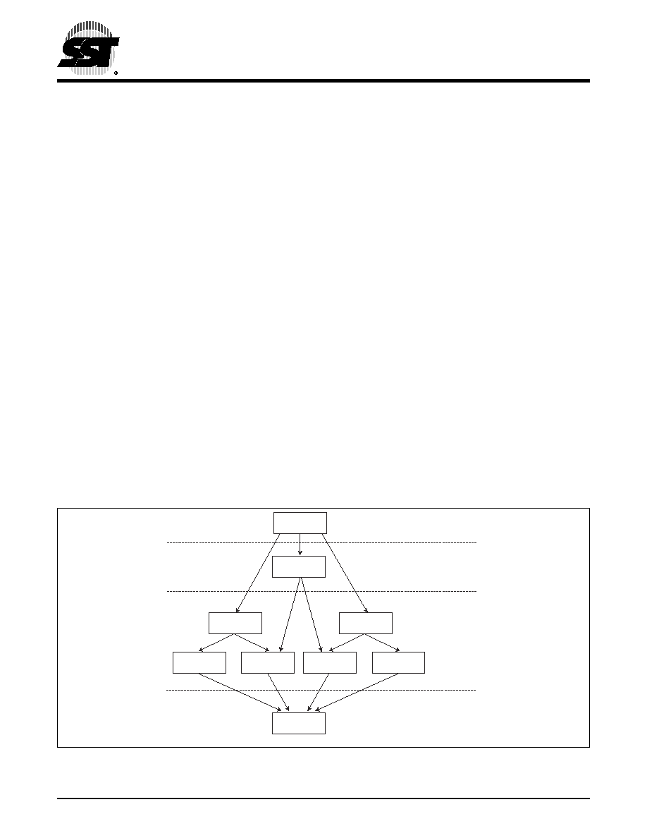
60
Preliminary Specifications
FlashFlex51 MCU
SST89E52RD2 / SST89E54RD2 / SST89E58RD2 / SST89E516RD2
SST89V52RD2 / SST89V54RD2 / SST89V58RD2 / SST89V516RD2
©2004 Silicon Storage Technology, Inc.
S71255-00-000
3/04
9.0 SECURITY LOCK
The security lock protects against software piracy and pre-
vents the contents of the flash from being read by unautho-
rized parties. It also protects against code corruption
resulting from accidental erasing and programming to the
internal flash memory. There are two different types of
security locks in the device security lock system: hard lock
and SoftLock.
9.1 Hard Lock
When hard lock is activated, MOVC or IAP instructions exe-
cuted from an unlocked or soft locked program address
space, are disabled from reading code bytes in hard locked
memory blocks (See Table 9-2). Hard lock can either lock
both flash memory blocks or just lock the 8 KByte flash
memory block (Block 1). All external host and IAP com-
mands except for Chip-Erase are ignored for memory
blocks that are hard locked.
9.2 SoftLock
SoftLock allows flash contents to be altered under a secure
environment. This lock option allows the user to update
program code in the soft locked memory block through in-
application programming mode under a predetermined
secure environment. For example, if Block 1 (8K) memory
block is locked (hard locked or soft locked), and Block 0
memory block is soft locked, code residing in Block 1 can
program Block 0. The following IAP mode commands
issued through the command mailbox register, SFCM, exe-
cuted from a Locked (hard locked or soft locked) block, can
be operated on a soft locked block: Block-Erase, Sector-
Erase, Byte-Program and Byte-Verify.
In external host mode, SoftLock behaves the same as a
hard lock.
9.3 Security Lock Status
The three bits that indicate the device security lock
status are located in SFST[7:5]. As shown in Figure 9-
1 and Table 9-1, the three security lock bits control the
lock status of the primary and secondary blocks of
memory. There are four distinct levels of security lock
status. In the first level, none of the security lock bits
are programmed and both blocks are unlocked. In the
second level, although both blocks are now locked and
cannot be programmed, they are available for read
operation via Byte-Verify. In the third level, three differ-
ent options are available: Block 1 hard lock / Block 0
SoftLock, SoftLock on both blocks, and hard lock on
both blocks. Locking both blocks is the same as Level
2, Block 1 except read operation isn't available. The
fourth level of security is the most secure level. It
doesn't allow read/program of internal memory or boot
from external memory. For details on how to program
the security lock bits refer to the external host mode
and in-application programming sections.
FIGURE
9-1: S
ECURITY
L
OCK
L
EVELS
Note:
P = Programmed (Bit logic state = 0), U = Unprogrammed (Bit logic state = 1), N = Not Locked, L = Hard locked, S = Soft locked
Level 1
Level 2
Level 3
Level 4
UUU/NN
PUU/SS
UPP/LL
PPU/LS
UPU/SS
PPP/LL
1255 F29.0
PUP/LL
UPP/LL
UUP/LS
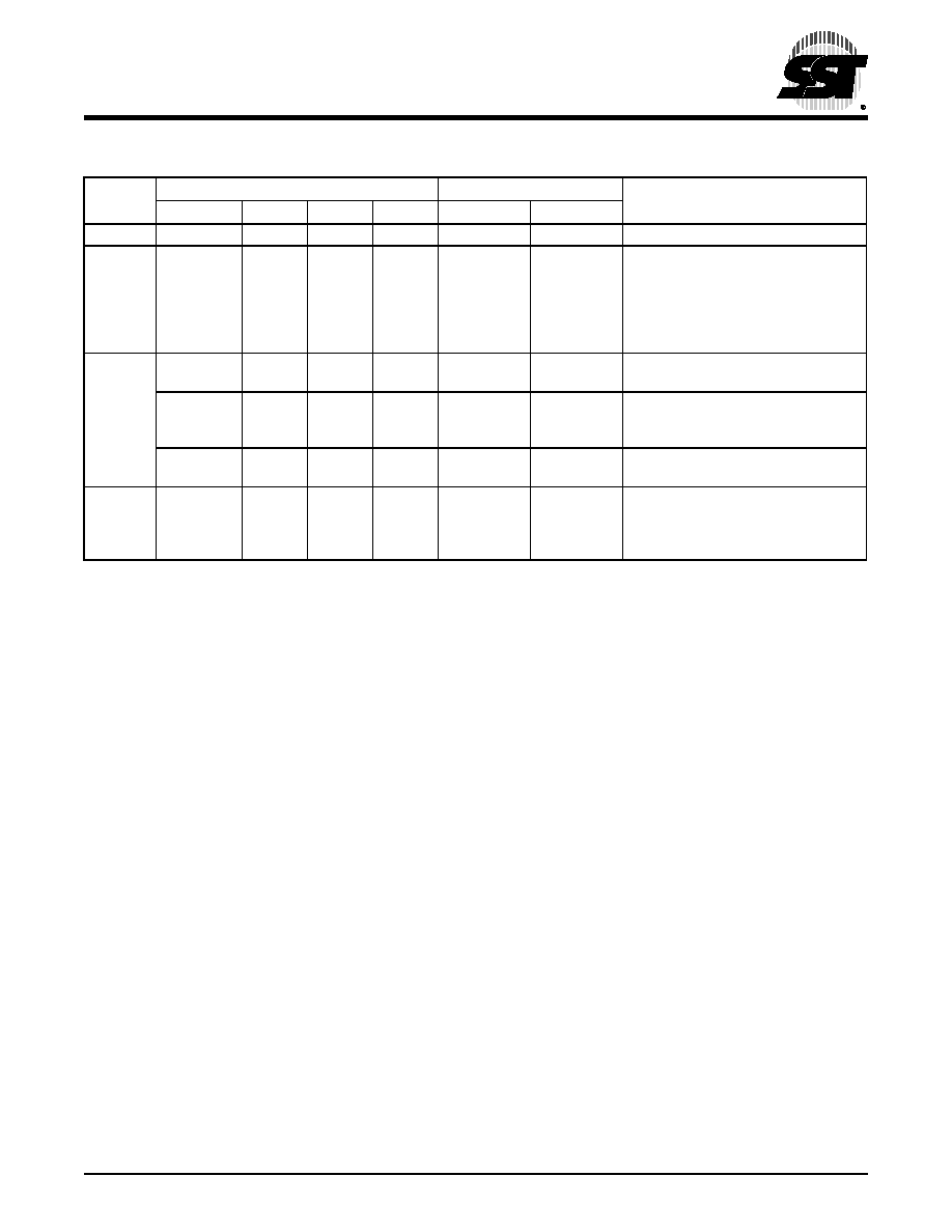
Preliminary Specifications
FlashFlex51 MCU
SST89E52RD2 / SST89E54RD2 / SST89E58RD2 / SST89E516RD2
SST89V52RD2 / SST89V54RD2 / SST89V58RD2 / SST89V516RD2
61
©2004 Silicon Storage Technology, Inc.
S71255-00-000
3/04
9.4 Read Operation Under Lock Condition
The status of security bits SB1, SB2, and SB3 can be read
when the read command is disabled by security lock.
There are three ways to read the status.
1. External host mode: Read-back = 00H (locked)
2. IAP command: Read-back = previous SFDT data
3. MOVC: Read-back = FFH (blank)
TABLE
9-1: S
ECURITY
L
OCK
O
PTIONS
Level
Security Lock Bits
1,2
Security Status of:
Security Type
SFST[7:5]
SB1
SB2
1
SB3
1
Block 1
Block 0
1
000
U
U
U
Unlock
Unlock
No Security Features are Enabled.
2
100
P
U
U
SoftLock
SoftLock
MOVC instructions executed from
external program memory are dis-
abled from fetching code bytes from
internal memory, EA# is sampled and
latched on Reset, and further pro-
gramming of the flash is disabled.
3
011
101
U
P
P
U
P
P
Hard Lock
Hard Lock
Level 2 plus Verify disabled, both
blocks locked.
010
U
P
U
SoftLock
SoftLock
Level 2 plus Verify disabled. Code in
Block 1 may program Block 0 and vice
versa.
110
001
P
U
P
U
U
P
Hard Lock
SoftLock
Level 2 plus Verify disabled. Code in
Block 1 may program Block 0.
4
111
P
P
P
Hard Lock
Hard Lock
Same as Level 3 hard lock/hard lock,
but MCU will start code execution
from the internal memory regardless
of EA#.
T9-1.0 1255
1. P = Programmed (Bit logic state = 0), U = Unprogrammed (Bit logic state = 1).
2. SFST[7:5] = Security Lock Status Bits (SB1_i, SB2_i, SB3_i)

62
Preliminary Specifications
FlashFlex51 MCU
SST89E52RD2 / SST89E54RD2 / SST89E58RD2 / SST89E516RD2
SST89V52RD2 / SST89V54RD2 / SST89V58RD2 / SST89V516RD2
©2004 Silicon Storage Technology, Inc.
S71255-00-000
3/04
TABLE
9-2: S
ECURITY
L
OCK
A
CCESS
T
ABLE
Level
SFST[7:5]
Source
Address
1
Target
Address
2
Byte-Verify Allowed
MOVC Allowed
External Host
3
IAP
516RD2
5xRD2
4
111b
(hard lock on both blocks)
Block 0/1
Block 0/1
N
N
Y
Y
External
N/A
N/A
N
Y
External
Block 0/1
N
N
N
N
External
N/A
N/A
N
Y
3
011b/101b
(hard lock on both blocks)
Block 0/1
Block 0/1
N
N
Y
Y
External
N/A
N/A
N
Y
External
Block 0/1
N
N
N
N
External
N/A
N/A
Y
Y
001b/110b
(Block 0 = SoftLock,
Block 1 = hard lock)
Block 0
Block 0
N
N
Y
Y
Block 1
N
N
N
N
External
N/A
N/A
N
Y
Block 1
Block 0
N
Y
Y
Y
Block 1
N
N
Y
Y
External
N/A
N/A
N
Y
External
Block 0/1
N
N
N
N
External
N/A
N/A
Y
Y
010b
(SoftLock on both blocks)
Block 0
Block 0
N
N
Y
Y
Block 1
N
Y
Y
Y
External
N/A
N/A
N
Y
Block 1
Block 0
N
Y
Y
Y
Block 1
N
N
Y
Y
External
N/A
N/A
N
Y
External
Block 0/1
N
N
N
N
External
N/A
N/A
Y
Y
2
100b
(SoftLock on both blocks)
Block 0
Block 0
Y
N
Y
Y
Block 1
Y
Y
Y
Y
External
N/A
N/A
N
Y
Block 1
Block 0
Y
Y
Y
Y
Block 1
Y
N
Y
Y
External
N/A
N/A
N
Y
External
Block 0/1
Y
N
N
N
External
N/A
N/A
Y
Y
1
000b
(unlock)
Block 0
Block 0
Y
N
Y
Y
Block 1
Y
Y
Y
Y
External
N/A
N/A
N
Y
Block 1
Block 0
Y
Y
Y
Y
Block 1
Y
N
Y
Y
External
N/A
N/A
N
Y
External
Block 0/1
Y
Y
N
Y
External
N/A
N/A
Y
Y
T9-2.0 1255
1. Location of MOVC or IAP instruction
2. Target address is the location of the byte being read
3. External host Byte-Verify access does not depend on a source address.

Preliminary Specifications
FlashFlex51 MCU
SST89E52RD2 / SST89E54RD2 / SST89E58RD2 / SST89E516RD2
SST89V52RD2 / SST89V54RD2 / SST89V58RD2 / SST89V516RD2
63
©2004 Silicon Storage Technology, Inc.
S71255-00-000
3/04
10.0 RESET
A system reset initializes the MCU and begins program
execution at program memory location 0000H. The reset
input for the device is the RST pin. In order to reset the
device, a logic level high must be applied to the RST pin for
at least two machine cycles (24 clocks), after the oscillator
becomes stable. ALE, PSEN# are weakly pulled high dur-
ing reset. During reset, ALE and PSEN# output a high level
in order to perform a proper reset. This level must not be
affected by external element. A system reset will not affect
the 1 KByte of on-chip RAM while the device is running,
however, the contents of the on-chip RAM during power up
are indeterminate. Following reset, all Special Function
Registers (SFR) return to their reset values outlined in
Tables 3-7 to 3-11.
10.1 Power-on Reset
At initial power up, the port pins will be in a random state
until the oscillator has started and the internal reset algo-
rithm has weakly pulled all pins high. Powering up the
device without a valid reset could cause the MCU to
start executing instructions from an indeterminate
location. Such undefined states may inadvertently cor-
rupt the code in the flash.
When power is applied to the device, the RST pin must be
held high long enough for the oscillator to start up (usually
several milliseconds for a low frequency crystal), in addition
to two machine cycles for a valid power-on reset. An exam-
ple of a method to extend the RST signal is to implement a
RC circuit by connecting the RST pin to V
DD
through a 10
µF capacitor and to V
SS
through an 8.2K
resistor as
shown in Figure 10-1. Note that if an RC circuit is being
used, provisions should be made to ensure the V
DD
rise
time does not exceed 1 millisecond and the oscillator start-
up time does not exceed 10 milliseconds.
For a low frequency oscillator with slow start-up time the
reset signal must be extended in order to account for the
slow start-up time. This method maintains the necessary
relationship between V
DD
and RST to avoid programming
at an indeterminate location, which may cause corruption
in the code of the flash. The power-on detection is
designed to work as power up initially, before the voltage
reaches the brown-out detection level. The POF flag in the
PCON register is set to indicate an initial power up condi-
tion. The POF flag will remain active until cleared by soft-
ware. Please refer to Section 3.5, PCON register definition
for detail information.
For more information on system level design techniques,
please review the
Design Considerations for the SST
FlashFlex51 Family Microcontroller
application note.
FIGURE
10-1: P
OWER
-
ON
R
ESET
C
IRCUIT
10.2 Software Reset
The software reset is executed by changing SFCF[1]
(SWR) from "0" to "1". A software reset will reset the pro-
gram counter to address 0000H. All SFR registers will be
set to their reset values, except SFCF[1] (SWR), WDTC[2]
(WDTS), and RAM data will not be altered.
10.3 Brown-out Detection Reset
The device includes a brown-out detection circuit to protect
the system from severed supplied voltage V
DD
fluctuations.
SST89E5xxRD2 internal brown-out detection threshold is
3.85V, SST89V5xxRD2 brown-out detection threshold is
2.35V. For brown-out voltage parameters, please refer to
Tables 14-6 and 14-7.
When V
DD
drops below this voltage threshold, the brown-
out detector triggers the circuit to generate a brown-out
interrupt but the CPU still runs until the supplied voltage
returns to the brown-out detection voltage V
BOD
. The
default operation for a brown-out detection is to cause a
processor reset.
V
DD
must stay below V
BOD
at least four oscillator clock peri-
ods before the brown-out detection circuit will respond.
Brown-out interrupt can be enabled by setting the EBO bit
in IEA register (address E8H, bit 3). If EBO bit is set and a
brown-out condition occurs, a brown-out interrupt will be
generated to execute the program at location 004BH. It is
required that the EBO bit be cleared by software after the
brown-out interrupt is serviced. Clearing EBO bit when the
brown-out condition is active will properly reset the device.
If brown-out interrupt is not enabled, a brown-out condition
will reset the program to resume execution at location
0000H.
1255 F30.0
V
DD
V
DD
10µF
+
-
8.2K
SST89E/V5xxRD2
RST
XTAL2
XTAL1
C
1
C
2

64
Preliminary Specifications
FlashFlex51 MCU
SST89E52RD2 / SST89E54RD2 / SST89E58RD2 / SST89E516RD2
SST89V52RD2 / SST89V54RD2 / SST89V58RD2 / SST89V516RD2
©2004 Silicon Storage Technology, Inc.
S71255-00-000
3/04
11.0 INTERRUPTS
11.1 Interrupt Priority and Polling Sequence
The device supports eight interrupt sources under a four level priority scheme. Table 11-1 summarizes the polling
sequence of the supported interrupts. Note that the SPI serial interface and the UART share the same interrupt
vector. (See Figure 11-1)
TABLE
11-1: I
NTERRUPT
P
OLLING
S
EQUENCE
Description
Interrupt Flag
Vector
Address
Interrupt
Enable
Interrupt
Priority
Service
Priority
Wake-Up
Power-down
Ext. Int0
IE0
0003H
EX0
PX0/H
1(highest)
yes
Brown-out
-
004BH
EBO
PBO/H
2
no
T0
TF0
000BH
ET0
PT0/H
3
no
Ext. Int1
IE1
0013H
EX1
PX1/H
4
yes
T1
TF1
001BH
ET1
PT1/H
5
no
PCA
CF/CCFn
0033H
EC
PPCH
6
no
Ext. Int. 2
IE2
003BH
EX2
PX2/H
7
no
Ext. Int. 3
IE3
0043H
EX3
PX3/H
8
no
UART/SPI
TI/RI/SPIF
0023H
ES
PS/H
9
no
T2
TF2, EXF2
002BH
ET2
PT2/H
10
no
T11-1.0 1255
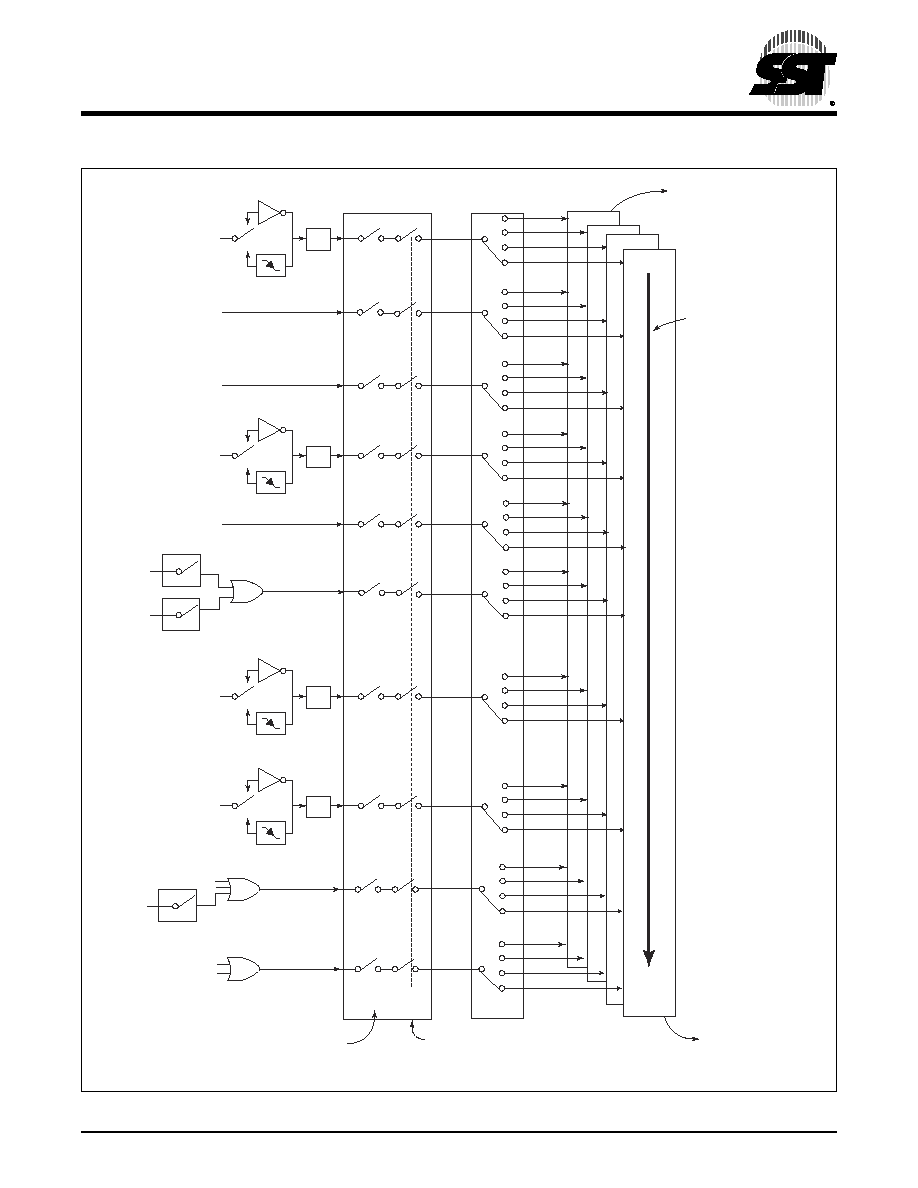
Preliminary Specifications
FlashFlex51 MCU
SST89E52RD2 / SST89E54RD2 / SST89E58RD2 / SST89E516RD2
SST89V52RD2 / SST89V54RD2 / SST89V58RD2 / SST89V516RD2
65
©2004 Silicon Storage Technology, Inc.
S71255-00-000
3/04
FIGURE
11-1: I
NTERRUPT
S
TRUCTURE
INTERRUPT
POLLING
SEQUENCE
IE1
INT1#
INDIVIDUAL
ENABLES
TF1
TF0
RI
0
1
IE0
GLOBAL
DISABLE
HIGHEST PRIORITY
INTERRUPT
LOWEST PRIORITY
INTERRUPT
IT0
IT1
INT0#
IE & IEA
REGISTERS
IP/IPH/IPA/IPAH
REGISTERS
0
1
TF2
EXF2
1255 F31.0
TI
SPIE
SPIF
BOF
CF
ECF
CCFn
ECCFn
IE2
IT2
INT2#
0
1
IE3
IT3
INT3#
0
1
66
Preliminary Specifications
FlashFlex51 MCU
SST89E52RD2 / SST89E54RD2 / SST89E58RD2 / SST89E516RD2
SST89V52RD2 / SST89V54RD2 / SST89V58RD2 / SST89V516RD2
©2004 Silicon Storage Technology, Inc.
S71255-00-000
3/04
12.0 POWER-SAVING MODES
The device provides two power saving modes of operation
for applications where power consumption is critical. The
two modes are idle and power-down, see Table 12-1.
12.1 Idle Mode
Idle mode is entered setting the IDL bit in the PCON regis-
ter. In idle mode, the program counter (PC) is stopped. The
system clock continues to run and all interrupts and periph-
erals remain active. The on-chip RAM and the special func-
tion registers hold their data during this mode.
The device exits idle mode through either a system inter-
rupt or a hardware reset. Exiting idle mode via system
interrupt, the start of the interrupt clears the IDL bit and
exits idle mode. After exit the Interrupt Service Routine, the
interrupted program resumes execution beginning at the
instruction immediately following the instruction which
invoked the idle mode. A hardware reset starts the device
similar to a power-on reset.
12.2 Power-down Mode
The power-down mode is entered by setting the PD bit in
the PCON register. In the power-down mode, the clock is
stopped and external interrupts are active for level sensitive
interrupts only. SRAM contents are retained during power-
down, the minimum V
DD
level is 2.0V.
The device exits power-down mode through either an
enabled external level sensitive interrupt or a hardware
reset. The start of the interrupt clears the PD bit and exits
power-down. Holding the external interrupt pin low restarts
the oscillator, the signal must hold low at least 1024 clock
cycles before bringing back high to complete the exit. Upon
interrupt signal being restored to logic V
IH,
the first instruc-
tion of the interrupt service routine will execute. A hardware
reset starts the device similar to power-on reset.
To exit properly out of power-down, the reset or external
interrupt should not be executed before the V
DD
line is
restored to its normal operating voltage. Be sure to hold
V
DD
voltage long enough at its normal operating level for
the oscillator to restart and stabilize (normally less than
10 ms).
TABLE
12-1: P
OWER
S
AVING
M
ODES
Mode
Initiated by
State of MCU
Exited by
Idle Mode
Software
(Set IDL bit in PCON)
MOV PCON, #01H;
CLK is running.
Interrupts, serial port and tim-
ers/counters are active. Pro-
gram Counter is stopped.
ALE and PSEN# signals at a
HIGH level during Idle. All
registers remain unchanged.
Enabled interrupt or hardware reset.
Start of interrupt clears IDL bit and
exits idle mode, after the ISR RETI
instruction, program resumes execu-
tion beginning at the instruction follow-
ing the one that invoked idle mode. A
user could consider placing two or
three NOP instructions after the
instruction that invokes idle mode to
eliminate any problems. A hardware
reset restarts the device similar to a
power-on reset.
Power-down
Mode
Software
(Set PD bit in PCON)
MOV PCON, #02H;
CLK is stopped. On-chip
SRAM and SFR data is main-
tained. ALE and PSEN# sig-
nals at a LOW level during
power -down. External Inter-
rupts are only active for level
sensitive interrupts, if
enabled.
Enabled external level sensitive inter-
rupt or hardware reset. Start of inter-
rupt clears PD bit and exits power-
down mode, after the ISR RETI
instruction program resumes execution
beginning at the instruction following
the one that invoked power-down
mode. A user could consider placing
two or three NOP instructions after the
instruction that invokes power-down
mode to eliminate any problems. A
hardware reset restarts the device sim-
ilar to a power-on reset.
T12-1.0 1255

Preliminary Specifications
FlashFlex51 MCU
SST89E52RD2 / SST89E54RD2 / SST89E58RD2 / SST89E516RD2
SST89V52RD2 / SST89V54RD2 / SST89V58RD2 / SST89V516RD2
67
©2004 Silicon Storage Technology, Inc.
S71255-00-000
3/04
13.0 SYSTEM CLOCK AND CLOCK OPTIONS
13.1 Clock Input Options and Recom-
mended Capacitor Values for Oscillator
Shown in Figure 13-1 are the input and output of an inter-
nal inverting amplifier (XTAL1, XTAL2), which can be con-
figured for use as an on-chip oscillator.
When driving the device from an external clock source,
XTAL2 should be left disconnected and XTAL1 should be
driven.
At start-up, the external oscillator may encounter a higher
capacitive load at XTAL1 due to interaction between the
amplifier and its feedback capacitance. However, the
capacitance will not exceed 15 pF once the external signal
meets the V
IL
and V
IH
specifications.
Crystal manufacturer, supply voltage, and other factors
may cause circuit performance to differ from one applica-
tion to another. C1 and C2 should be adjusted appropri-
ately for each design. Table 13-1, shows the typical values
for C1 and C2 vs. crystal type for various frequencies
More specific information about on-chip oscillator design
can be found in the
FlashFlex51 Oscillator Circuit Design
Considerations
application note.
13.2 Clock Doubling Option
By default, the device runs at 12 clocks per machine cycle
(x1 mode). The device has a clock doubling option to
speed up to 6 clocks per machine cycle. Please refer to
Table 13-2 for detail.
Clock double mode can be enabled either via the external
host mode or the IAP mode. Please refer to Table 4-1 for
the external host mode enabling command and to Table 4-
6 and Table 4-7 for the IAP mode enabling commands
(When set, the EDC# bit in SFST register will indicate 6
clock mode.).
The clock double mode is only for doubling the inter-
nal system clock and the internal flash memory, i.e.
EA#=1. To access the external memory and the peripheral
devices, careful consideration must be taken. Also note
that the crystal output (XTAL2) will not be doubled.
FIGURE
13-1: O
SCILLATOR
C
HARACTERISTICS
TABLE
13-1:R
ECOMMENDED
V
ALUES
FOR
C1
AND
C2
BY
C
RYSTAL
T
YPE
Crystal
C1 = C2
Quartz
20-30pF
Ceramic
40-50pF
T13-1.0 1255
TABLE
13-2: C
LOCK
D
OUBLING
F
EATURES
Device
Standard Mode (x1)
Clock Double Mode (x2)
Clocks per
Machine Cycle
Max. External Clock Frequency
(MHz)
Clocks per
Machine Cycle
Max. External Clock Frequency
(MHz)
SST89E5xxRD2
12
40
6
20
SST89V5xxRD2
12
33
6
16
T13-2.0 1255
1255 F32.0
XTAL2
XTAL1
V
SS
C1
Using the On-Chip Oscillator
External Clock Drive
C2
XTAL2
XTAL1
V
SS
External
Oscillator
Signal
NC

68
Preliminary Specifications
FlashFlex51 MCU
SST89E52RD2 / SST89E54RD2 / SST89E58RD2 / SST89E516RD2
SST89V52RD2 / SST89V54RD2 / SST89V58RD2 / SST89V516RD2
©2004 Silicon Storage Technology, Inc.
S71255-00-000
3/04
14.0 ELECTRICAL SPECIFICATION
Note: This specification contains preliminary information on new products in production.
The specifications are subject to change without notice.
Absolute Maximum Stress Ratings (Applied conditions greater than those listed under "Absolute Maximum
Stress Ratings" may cause permanent damage to the device. This is a stress rating only and functional operation
of the device at these conditions or conditions greater than those defined in the operational sections of this data
sheet is not implied. Exposure to absolute maximum stress rating conditions may affect device reliability.)
Ambient Temperature Under Bias . . . . . . . . . . . . . . . . . . . . . . . . . . . . . . . . . . . . . . . . . . . . . . . . . . -55∞C to +125∞C
Storage Temperature . . . . . . . . . . . . . . . . . . . . . . . . . . . . . . . . . . . . . . . . . . . . . . . . . . . . . . . . . . . . -65∞C to +150∞C
Voltage on EA# Pin to V
SS
. . . . . . . . . . . . . . . . . . . . . . . . . . . . . . . . . . . . . . . . . . . . . . . . . . . . . . . . . -0.5V to +14.0V
D.C. Voltage on Any Pin to Ground Potential . . . . . . . . . . . . . . . . . . . . . . . . . . . . . . . . . . . . . . . . . -0.5V to V
DD
+0.5V
Transient Voltage (<20ns) on Any Other Pin to V
SS
. . . . . . . . . . . . . . . . . . . . . . . . . . . . . . . . . . . . -1.0V to V
DD
+1.0V
Maximum I
OL
per I/O Pins P1.5, P1.6, P1.7. . . . . . . . . . . . . . . . . . . . . . . . . . . . . . . . . . . . . . . . . . . . . . . . . . . . 20mA
Maximum I
OL
per I/O for All Other Pins . . . . . . . . . . . . . . . . . . . . . . . . . . . . . . . . . . . . . . . . . . . . . . . . . . . . . . . 15mA
Package Power Dissipation Capability (T
a
= 25∞C) . . . . . . . . . . . . . . . . . . . . . . . . . . . . . . . . . . . . . . . . . . . . . . 1.5W
Through Hole Lead Soldering Temperature (10 Seconds). . . . . . . . . . . . . . . . . . . . . . . . . . . . . . . . . . . . . . . . 300∞C
Surface Mount Lead Soldering Temperature (3 Seconds) . . . . . . . . . . . . . . . . . . . . . . . . . . . . . . . . . . . . . . . . 240∞C
Output Short Circuit Current
1
. . . . . . . . . . . . . . . . . . . . . . . . . . . . . . . . . . . . . . . . . . . . . . . . . . . . . . . . . . . . . 50 mA
1. Outputs shorted for no more than one second. No more than one output shorted at a time.
(Based on package heat transfer limitations, not device power consumption.
TABLE
14-1: O
PERATING
R
ANGE
Symbol
Description
Min.
Max
Unit
T
a
Ambient Temperature Under Bias
Standard
0
+70
∞
C
Industrial
-40
+85
∞
C
V
DD
Supply Voltage
SST89E5xxRD2
4.5
5.5
V
SST89V5xxRD2
2.7
3.6
V
f
OSC
Oscillator Frequency
SST89E5xxRD2
0
40
MHz
SST89V5xxRD2
0
33
MHz
Oscillator Frequency for IAP
SST89E5xxRD2
.25
40
MHz
SST89V5xxRD2
.25
33
MHz
T14-1.0 1255
TABLE
14-2: R
ELIABILITY
C
HARACTERISTICS
Symbol
Parameter
Minimum Specification
Units
Test Method
N
END
1
1. This parameter is measured only for initial qualification and after a design or process change that could affect this parameter.
Endurance
10,000
Cycles
JEDEC Standard A117
T
DR
1
Data Retention
100
Years
JEDEC Standard A103
I
LTH
1
Latch Up
100 + I
DD
mA
JEDEC Standard 78
T14-2.0 1255
Preliminary Specifications
FlashFlex51 MCU
SST89E52RD2 / SST89E54RD2 / SST89E58RD2 / SST89E516RD2
SST89V52RD2 / SST89V54RD2 / SST89V58RD2 / SST89V516RD2
69
©2004 Silicon Storage Technology, Inc.
S71255-00-000
3/04
TABLE
14-3: AC C
ONDITIONS
OF
T
EST
Input Rise/Fall Time . . . . . . . . . . . . . . . 10 ns
Output Load . . . . . . . . . . . . . . . . . . . . . C
L
= 100 pF
See Figures 14-8 and 14-10
T14-3.0 1255
TABLE
14-4: R
ECOMMENDED
S
YSTEM
P
OWER
-
UP
T
IMINGS
Symbol
Parameter
Minimum
Units
T
PU-READ
1
1. This parameter is measured only for initial qualification and after a design or process change that could affect this parameter
Power-up to Read Operation
100
µs
T
PU-WRITE
1
Power-up to Write Operation
100
µs
T14-4.0 1255
TABLE
14-5: P
IN
I
MPEDANCE
(V
DD
=3.3V, Ta=25 ∞C, f=1 Mhz, other pins open)
Parameter
Description
Test Condition
Maximum
C
I/O
1
1. This parameter is measured only for initial qualification and after a design or process change that could affect this parameter.
I/O Pin Capacitance
V
I/O
= 0V
15 pF
C
IN
1
Input Capacitance
V
IN
= 0V
12 pF
L
PIN
2
2. Refer to PCI spec.
Pin Inductance
20 nH
T14-5.0 1255

70
Preliminary Specifications
FlashFlex51 MCU
SST89E52RD2 / SST89E54RD2 / SST89E58RD2 / SST89E516RD2
SST89V52RD2 / SST89V54RD2 / SST89V58RD2 / SST89V516RD2
©2004 Silicon Storage Technology, Inc.
S71255-00-000
3/04
14.1 DC Electrical Characteristics
TABLE
14-6: DC E
LECTRICAL
C
HARACTERISTICS
FOR
SST89E5
XX
RD2
T
a
= -40∞C
TO
+85∞C; V
DD
= 4.5-5.5V; V
SS
= 0V
Symbol
Parameter
Test Conditions
Min
Max
Units
V
IL
Input Low Voltage
4.5 < V
DD
< 5.5
-0.5
0.2V
DD
- 0.1
V
V
IH
Input High Voltage
4.5 < V
DD
< 5.5
0.2V
DD
+ 0.9
V
DD
+ 0.5
V
V
IH1
Input High Voltage (XTAL1, RST)
4.5 < V
DD
< 5.5
0.7V
DD
V
DD
+ 0.5
V
V
OL
Output Low Voltage (Ports 1.5, 1.6, 1.7)
V
DD
= 4.5V
I
OL
= 16mA
1.0
V
V
OL
Output Low Voltage (Ports 1, 2, 3)
1
V
DD
= 4.5V
I
OL
= 100µA
2
0.3
V
I
OL
= 1.6mA
2
0.45
V
I
OL
= 3.5mA
2
1.0
V
V
OL1
Output Low Voltage (Port 0, ALE, PSEN#)
1,3
V
DD
= 4.5V
I
OL
= 200µA
2
0.3
V
I
OL
= 3.2mA
2
0.45
V
V
OH
Output High Voltage (Ports 1, 2, 3, ALE, PSEN#)
4
V
DD
= 4.5V
I
OH
= -10µA
V
DD
- 0.3
V
I
OH
= -30µA
V
DD
- 0.7
V
I
OH
= -60µA
V
DD
- 1.5
V
V
OH1
Output High Voltage (Port 0 in External Bus Mode)
4
V
DD
= 4.5V
I
OH
= -200µA
V
DD
- 0.3
V
I
OH
= -3.2mA
V
DD
- 0.7
V
V
BOD
Brown-out Detection Voltage
3.85
4.15
V
I
IL
Logical 0 Input Current (Ports 1, 2, 3)
V
IN
= 0.4V
-75
µA
I
TL
Logical 1-to-0 Transition Current (Ports 1, 2, 3)
5
V
IN
= 2V
-650
µA
I
LI
Input Leakage Current (Port 0)
0.45 < V
IN
< V
DD
-0.3
±10
µA
R
RST
RST Pull-down Resistor
40
225
K
C
IO
Pin Capacitance
6
@ 1 MHz, 25∞C
15
pF
I
DD
Power Supply Current
IAP Mode
@ 12 MHz
70
mA
@ 40 MHz
88
mA
Active Mode
@ 12 MHz
23
mA
@ 40 MHz
50
mA
Idle Mode
@ 12 MHz
20
mA
@ 40 MHz
42
mA
Power-down Mode (min. V
DD
= 2V)
T
a
= 0∞C to +70∞C
80
µA
T
a
= -40∞C to +85∞C
90
µA
T14-6.0 1255

Preliminary Specifications
FlashFlex51 MCU
SST89E52RD2 / SST89E54RD2 / SST89E58RD2 / SST89E516RD2
SST89V52RD2 / SST89V54RD2 / SST89V58RD2 / SST89V516RD2
71
©2004 Silicon Storage Technology, Inc.
S71255-00-000
3/04
1. Under steady state (non-transient) conditions, I
OL
must be externally limited as follows:
Maximum I
OL
per port pin:
15mA
Maximum I
OL
per 8-bit port:26mA
Maximum I
OL
total for all outputs:71mA
If I
OL
exceeds the test condition, V
OL
may exceed the related specification.
Pins are not guaranteed to sink current greater than the listed test conditions.
2. Capacitive loading on Ports 0 & 2 may cause spurious noise to be superimposed on the V
OL
s of ALE and Ports 1 & 3. The noise due
to external bus capacitance discharging into the Port 0 & 2 pins when the pins make 1-to-0 transitions during bus operations. In the
worst cases (capacitive loading > 100pF), the noise pulse on the ALE pin may exceed 0.8V. In such cases, it may be desirable to
qualify ALE with a Schmitt Trigger, or use an address latch with a Schmitt Trigger STROBE input.
3. Load capacitance for Port 0, ALE & PSEN#= 100pF, load capacitance for all other outputs = 80pF.
4. Capacitive loading on Ports 0 & 2 may cause the V
OH
on ALE and PSEN# to momentarily fall below the V
DD
- 0.7 specification when
the address bits are stabilizing.
5. Pins of Ports 1, 2 & 3 source a transition current when they are being externally driven from 1 to 0. The transition current reaches its
maximum value when V
IN
is approximately 2V.
6. Pin capacitance is characterized but not tested. EA# is 25pF (max).

72
Preliminary Specifications
FlashFlex51 MCU
SST89E52RD2 / SST89E54RD2 / SST89E58RD2 / SST89E516RD2
SST89V52RD2 / SST89V54RD2 / SST89V58RD2 / SST89V516RD2
©2004 Silicon Storage Technology, Inc.
S71255-00-000
3/04
TABLE
14-7: DC E
LECTRICAL
C
HARACTERISTICS
FOR
SST89V5
XX
RD2
T
a
= -40∞C
TO
+85∞C; V
DD
= 2.7-3.6V; V
SS
= 0V
Symbol
Parameter
Test Conditions
Min
Max
Units
V
IL
Input Low Voltage
2.7 < V
DD
< 3.6
-0.5
0.7
V
V
IH
Input High Voltage
2.7 < V
DD
< 3.6
0.2V
DD
+ 0.9
V
DD
+ 0.5
V
V
IH1
Input High Voltage (XTAL1, RST)
2.7 < V
DD
< 3.6
0.7V
DD
V
DD
+ 0.5
V
V
OL
Output Low Voltage (Ports 1.5, 1.6, 1.7)
V
DD
= 2.7V
I
OL
= 16mA
1.0
V
V
OL
Output Low Voltage (Ports 1, 2, 3)
1
V
DD
= 2.7V
I
OL
= 100µA
2
0.3
V
I
OL
= 1.6mA
2
0.45
V
I
OL
= 3.5mA
2
1.0
V
V
OL1
Output Low Voltage (Port 0, ALE, PSEN#)
1,3
V
DD
= 2.7V
I
OL
= 200µA
2
0.3
V
I
OL
= 3.2mA
2
0.45
V
V
OH
Output High Voltage (Ports 1, 2, 3, ALE, PSEN#)
4
V
DD
= 2.7V
I
OH
= -10µA
V
DD
- 0.3
V
I
OH
= -30µA
V
DD
- 0.7
V
I
OH
= -60µA
V
DD
- 1.5
V
V
OH1
Output High Voltage (Port 0 in External Bus Mode)
4
V
DD
= 2.7V
I
OH
= -200µA
V
DD
- 0.3
V
I
OH
= -3.2mA
V
DD
- 0.7
V
V
BOD
Brown-out Detection Voltage
2.35
2.55
V
I
IL
Logical 0 Input Current (Ports 1, 2, 3)
V
IN
= 0.4V
-75
µA
I
TL
Logical 1-to-0 Transition Current (Ports 1, 2, 3)
5
V
IN
= 2V
-650
µA
I
LI
Input Leakage Current (Port 0)
0.45 < V
IN
< V
DD
-0.3
±10
µA
R
RST
RST Pull-down Resistor
225
K
C
IO
Pin Capacitance
6
@ 1 MHz, 25∞C
15
pF
I
DD
Power Supply Current
IAP Mode
@ 12 MHz
40
mA
@ 33 MHz
47
mA
Active Mode
@ 12 MHz
11.5
mA
@ 33 MHz
30
mA
Idle Mode
@ 12 MHz
8.5
mA
@ 33 MHz
21
mA
Power-down Mode (min. V
DD
= 2V)
T
a
= 0∞C to +70∞C
45
µA
T
a
= -40∞C to +85∞C
55
µA
T14-7.0 1255
1. Under steady state (non-transient) conditions, I
OL
must be externally limited as follows:
Maximum I
OL
per port pin:
15mA
Maximum I
OL
per 8-bit port:
26mA
Maximum I
OL
total for all outputs: 71mA
If I
OL
exceeds the test condition, V
OL
may exceed the related specification. Pins are not guaranteed to sink current greater than the
listed test conditions.

Preliminary Specifications
FlashFlex51 MCU
SST89E52RD2 / SST89E54RD2 / SST89E58RD2 / SST89E516RD2
SST89V52RD2 / SST89V54RD2 / SST89V58RD2 / SST89V516RD2
73
©2004 Silicon Storage Technology, Inc.
S71255-00-000
3/04
2. Capacitive loading on Ports 0 & 2 may cause spurious noise to be superimposed on the V
OL
s of ALE and Ports 1 & 3. The noise due
to external bus capacitance discharging into the Port 0 & 2 pins when the pins make 1-to-0 transitions during bus operations. In the
worst cases (capacitive loading > 100pF), the noise pulse on the ALE pin may exceed 0.8V. In such cases, it may be desirable to
qualify ALE with a Schmitt Trigger, or use an address latch with a Schmitt Trigger STROBE input.
3. Load capacitance for Port 0, ALE & PSEN#= 100pF, load capacitance for all other outputs = 80pF.
4. Capacitive loading on Ports 0 & 2 may cause the V
OH
on ALE and PSEN# to momentarily fall below the V
DD
- 0.7 specification when
the address bits are stabilizing.
5. Pins of Ports 1, 2 & 3 source a transition current when they are being externally driven from 1 to 0. The transition current reaches its
maximum value when V
IN
is approximately 2V.
6. Pin capacitance is characterized but not tested. EA# is 25pF (max).
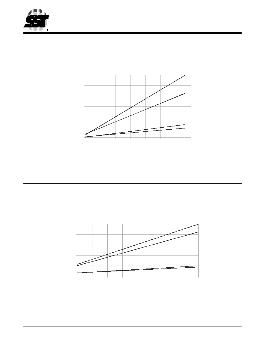
74
Preliminary Specifications
FlashFlex51 MCU
SST89E52RD2 / SST89E54RD2 / SST89E58RD2 / SST89E516RD2
SST89V52RD2 / SST89V54RD2 / SST89V58RD2 / SST89V516RD2
©2004 Silicon Storage Technology, Inc.
S71255-00-000
3/04
FIGURE
14-1: I
DD
VS
. F
REQUENCY
FOR
3V SST89V5
XX
RD2
FIGURE
14-2: I
DD
VS
. F
REQUENCY
FOR
5V SST89E5
XX
RD2
30
25
20
15
10
5
0
5
10
15
20
25
30
35
I
DD
(mA)
Internal Clock Frequency (MHz)
Maximum Idle I
DD
Typical Idle I
DD
Maximum Active I
DD
Typical Active I
DD
1255 F33.0
50
40
30
20
10
0
5
10
15
20
25
30
35
40
I
DD
(mA)
Internal Clock Frequency (MHz)
1255 F34.0
Maximum Idle I
DD
Typical Idle I
DD
Maximum Active I
DD
Typical Active I
DD

Preliminary Specifications
FlashFlex51 MCU
SST89E52RD2 / SST89E54RD2 / SST89E58RD2 / SST89E516RD2
SST89V52RD2 / SST89V54RD2 / SST89V58RD2 / SST89V516RD2
75
©2004 Silicon Storage Technology, Inc.
S71255-00-000
3/04
14.2 AC Electrical Characteristics
AC Characteristics: (Over Operating Conditions: Load Capacitance for Port 0, ALE#, and PSEN# = 100pF;
Load Capacitance for All Other Outputs = 80pF)
TABLE
14-8: AC E
LECTRICAL
C
HARACTERISTICS
(1
OF
2)
T
a
= -40∞C
TO
+85∞C, V
DD
= 2.7-3.6V@33MH
Z
, 4.5-5.5V@40MH
Z
, V
SS
= 0V
Symbol
Parameter
Oscillator
Units
33 MHz (x1 Mode)
16 MHz (x2 Mode)
1
40 MHz (x1 Mode)
20 MHz (x2 Mode)
1
Variable
Min
Max
Min
Max
Min
Max
1/T
CLCL
x1 Mode Oscillator Frequency
0
33
0
40
0
40
MHz
1/2T
CLCL
x2 Mode Oscillator Frequency
0
16
0
20
0
20
MHz
T
LHLL
ALE Pulse Width
46
35
2T
CLCL
- 15
ns
T
AVLL
Address Valid to ALE Low
5
T
CLCL
- 25 (3V)
ns
10
T
CLCL
- 15 (5V)
ns
T
LLAX
Address Hold After ALE Low
5
T
CLCL
- 25 (3V)
ns
10
T
CLCL
- 15 (5V)
ns
T
LLIV
ALE Low to Valid Instr In
56
4T
CLCL
- 65 (3V)
ns
55
4T
CLCL
- 45 (5V)
ns
T
LLPL
ALE Low to PSEN# Low
5
T
CLCL
- 25 (3V)
ns
10
T
CLCL
- 15 (5V)
ns
T
PLPH
PSEN# Pulse Width
66
60
3T
CLCL
- 25 (3V)
3T
CLCL
- 15 (5V)
ns
T
PLIV
PSEN# Low to Valid Instr In
35
3T
CLCL
- 55 (3V)
ns
25
3T
CLCL
- 50 (5V)
ns
T
PXIX
Input Instr Hold After PSEN#
0
ns
T
PXIZ
Input Instr Float After PSEN#
25
T
CLCL
- 5 (3V)
ns
10
T
CLCL
- 15 (5V)
ns
T
PXAV
PSEN# to Address valid
22
17
T
CLCL
- 8
ns
T
AVIV
Address to Valid Instr In
72
5T
CLCL
- 80 (3V)
ns
65
5T
CLCL
- 60 (5V)
ns
T
PLAZ
PSEN# Low to Address Float
10
10
10
ns
T
RLRH
RD# Pulse Width
142
120
6T
CLCL
- 40 (3V)
6T
CLCL
- 30 (5V)
ns
T
WLWH
Write Pulse Width (WE#)
142
120
6T
CLCL
- 40 (3V)
6T
CLCL
- 30 (5V)
ns
T
RLDV
RD# Low to Valid Data In
62
5T
CLCL
- 90 (3V)
ns
75
5T
CLCL
- 50 (5V)
ns
T
RHDX
Data Hold After RD#
0
0
0
ns
T
RHDZ
Data Float After RD#
36
2T
CLCL
- 25 (3V)
ns
38
2T
CLCL
- 12 (5V)
ns
T
LLDV
ALE Low to Valid Data In
152
8T
CLCL
- 90 (3V)
ns
150
8T
CLCL
- 50 (5V)
ns
T
AVDV
Address to Valid Data In
183
9T
CLCL
- 90 (3V)
ns
150
9T
CLCL
- 75 (5V)
ns
T
LLWL
ALE Low to RD# or WR# Low
66
116
60
90
3T
CLCL
- 25 (3V)
3T
CLCL
- 15 (5V)
3T
CLCL
+ 25 (3V)
3T
CLCL
+ 15 (5V)
ns
T
AVWL
Address to RD# or WR# Low
46
4T
CLCL
- 75 (3V)
ns
70
4T
CLCL
- 30 (5V)
ns

76
Preliminary Specifications
FlashFlex51 MCU
SST89E52RD2 / SST89E54RD2 / SST89E58RD2 / SST89E516RD2
SST89V52RD2 / SST89V54RD2 / SST89V58RD2 / SST89V516RD2
©2004 Silicon Storage Technology, Inc.
S71255-00-000
3/04
Explanation of Symbols Each timing symbol has 5 characters. The first character is always a `T' (stands for
time). The other characters, depending on their positions, stand for the name of a signal or the logical status of that
signal. The following is a list of all the characters and what they stand for.
For example:
T
AVLL
= Time from Address Valid to ALE Low
T
LLPL
= Time from ALE Low to PSEN# Low
T
WHQX
Data Hold After WR#
3
T
CLCL
- 27 (3V)
ns
5
T
CLCL
- 20 (5V)
ns
T
QVWH
Data Valid to WR# High
142
7T
CLCL
- 70 (3V)
ns
125
7T
CLCL
- 50 (5V)
ns
T
QVWX
Data Valid to WR# High to Low
Transition
10
5
T
CLCL
- 20
ns
T
RLAZ
RD# Low to Address Float
0
0
0
ns
T
WHLH
RD# to WR# High to ALE High
5
55
T
CLCL
- 25 (3V)
T
CLCL
+ 25 (3V)
ns
10
40
T
CLCL
- 15 (5V)
T
CLCL
+ 15 (5V)
ns
T14-8.0 1255
1. Calculated values are for x1 Mode only
A: Address
Q: Output data
C: Clock
R: RD# signal
D: Input data
T: Time
H: Logic level HIGH
V: Valid
I:
Instruction (program memory contents)
W: WR# signal
L: Logic level LOW or ALE
X: No longer a valid logic level
P: PSEN#
Z: High Impedance (Float)
TABLE
14-8: AC E
LECTRICAL
C
HARACTERISTICS
(C
ONTINUED
) (2
OF
2)
T
a
= -40∞C
TO
+85∞C, V
DD
= 2.7-3.6V@33MH
Z
, 4.5-5.5V@40MH
Z
, V
SS
= 0V
Symbol
Parameter
Oscillator
Units
33 MHz (x1 Mode)
16 MHz (x2 Mode)
1
40 MHz (x1 Mode)
20 MHz (x2 Mode)
1
Variable
Min
Max
Min
Max
Min
Max

Preliminary Specifications
FlashFlex51 MCU
SST89E52RD2 / SST89E54RD2 / SST89E58RD2 / SST89E516RD2
SST89V52RD2 / SST89V54RD2 / SST89V58RD2 / SST89V516RD2
77
©2004 Silicon Storage Technology, Inc.
S71255-00-000
3/04
FIGURE
14-3: E
XTERNAL
P
ROGRAM
M
EMORY
R
EAD
C
YCLE
FIGURE
14-4: E
XTERNAL
D
ATA
M
EMORY
R
EAD
C
YCLE
1255 F35.0
PORT 2
PORT 0
PSEN#
ALE
A0 - A7
TLLAX
TPLAZ
TPXIZ
TLLPL
TAVIV
TAVLL
TPXIX
TLHLL
TLLIV
TPLIV
TPLPH
INSTR IN
A8 - A15
A8 - A15
A0 - A7
TPXAV
1255 F36.0
PORT 2
PORT 0
RD#
PSEN#
ALE
TLHLL
P2[7:0] or A8-A15 FROM DPH
A0-A7 FROM RI or DPL
TAVDV
TAVWL
DATA IN
INSTR IN
TRLAZ
TAVLL
TLLAX
TLLWL
TLLDV
TRLRH
TRLDV
TRHDZ
TWHLH
TRHDX
A8-A15 FROM PCH
A0-A7 FROM PCL

78
Preliminary Specifications
FlashFlex51 MCU
SST89E52RD2 / SST89E54RD2 / SST89E58RD2 / SST89E516RD2
SST89V52RD2 / SST89V54RD2 / SST89V58RD2 / SST89V516RD2
©2004 Silicon Storage Technology, Inc.
S71255-00-000
3/04
FIGURE
14-5: E
XTERNAL
D
ATA
M
EMORY
W
RITE
C
YCLE
FIGURE
14-6: E
XTERNAL
C
LOCK
D
RIVE
W
AVEFORM
TABLE
14-9: E
XTERNAL
C
LOCK
D
RIVE
Symbol
Parameter
Oscillator
Units
12MHz
40MHz
Variable
Min
Max
Min
Max
Min
Max
1/T
CLCL
Oscillator Frequency
0
40
MHz
T
CLCL
83
25
ns
T
CHCX
High Time
8.75
0.35T
CLCL
0.65T
CLCL
ns
T
CLCX
Low Time
8.75
0.35T
CLCL
0.65T
CLCL
ns
T
CLCH
Rise Time
20
10
ns
T
CHCL
Fall Time
20
10
ns
T14-9.0 1255
1255 F37.0
PORT 2
PORT 0
WR#
PSEN#
ALE
TLHLL
P2[7:0] or A8-A15 FROM DPH
A0-A7 FROM RI or DPL
DATA OUT
INSTR IN
TAVLL
TAVWL
TLLWL
TLLAX
TWLWH
TQVWH
TWHQX
TQVWX
TWHLH
A8-A15 FROM PCH
A0-A7 FROM PCL
0.2 VDD - 0.1
0.45 V
TCHCL
TCLCL
TCLCH
TCLCX
TCHCX
0.7VDD
VDD - 0.5
1255 F38.0

Preliminary Specifications
FlashFlex51 MCU
SST89E52RD2 / SST89E54RD2 / SST89E58RD2 / SST89E516RD2
SST89V52RD2 / SST89V54RD2 / SST89V58RD2 / SST89V516RD2
79
©2004 Silicon Storage Technology, Inc.
S71255-00-000
3/04
FIGURE
14-7: S
HIFT
R
EGISTER
M
ODE
T
IMING
W
AVEFORMS
FIGURE
14-8: AC T
ESTING
I
NPUT
/O
UTPUT
T
EST
W
AVEFORM
FIGURE
14-9: F
LOAT
W
AVEFORM
TABLE 14-10: S
ERIAL
P
ORT
T
IMING
Symbol
Parameter
Oscillator
Units
12MHz
40MHz
Variable
Min
Max
Min
Max
Min
Max
T
XLXL
Serial Port Clock Cycle Time
1.0
0.3
12T
CLCL
µs
T
QVXH
Output Data Setup to Clock Rising Edge
700
117
10T
CLCL
- 133
ns
T
XHQX
Output Data Hold After Clock Rising Edge
50
2T
CLCL
- 117
ns
0
2T
CLCL
- 50
ns
T
XHDX
Input Data Hold After Clock Rising Edge
0
0
0
ns
T
XHDV
Clock Rising Edge to Input Data Valid
700
117
10T
CLCL
- 133
ns
T14-10.0 1255
1255 F39.0
ALE
0
INSTRUCTION
CLOCK
OUTPUT DATA
WRITE TO SBUF
VALID
VALID
VALID
VALID
VALID
VALID
VALID
VALID
INPUT DATA
CLEAR RI
0
1
2
3
4
5
6
7
T
XLXL
T
QVXH
TXHQX
TXHDV
TXHDX
SET TI
SET R I
1
2
3
4
5
6
7
8
VLT
AC Inputs during testing are driven at VIHT (VDD -0.5V) for Logic "1" and
VILT (0.45V) for a Logic "0". Measurement reference points for inputs and
outputs are at VHT (0.2VDD + 0.9) and VLT (0.2VDD - 0.1)
VHT
VIHT
VILT
1255 F40.0
Note: VHT- VHIGH Test
VLT- VLOW Test
VIHT-VINPUT HIGH Test
VILT- VINPUT LOW Test
For timing purposes, a port pin is no longer floating when a 100 mV
change from load voltage occurs, and begins to float when a 100 mV
change from the loaded VOH/VOL level occurs. IOL/IOH = ± 20mA.
VLOAD +0.1V
VLOAD -0.1V
VOH -0.1V
Timing Reference
Points
VOL +0.1V
VLOAD
1255 F41.0

80
Preliminary Specifications
FlashFlex51 MCU
SST89E52RD2 / SST89E54RD2 / SST89E58RD2 / SST89E516RD2
SST89V52RD2 / SST89V54RD2 / SST89V58RD2 / SST89V516RD2
©2004 Silicon Storage Technology, Inc.
S71255-00-000
3/04
FIGURE 14-10: A T
EST
L
OAD
E
XAMPLE
FIGURE 14-11: I
DD
T
EST
C
ONDITION
,
A
CTIVE
M
ODE
FIGURE 14-12: I
DD
T
EST
C
ONDITION
,
I
DLE
M
ODE
FIGURE 14-13: I
DD
T
EST
C
ONDITION
,
P
OWER
-
DOWN
M
ODE
1255 F42.0
TO TESTER
TO DUT
CL
VDD
VDD
VDD
VDD
P0
EA#
RST
XTAL2
(NC)
CLOCK
SIGNAL
All other pins disconnected
SST89x5xxRD2
XTAL1
1255 F43.0
VSS
IDD
VDD
VDD
VDD
P0
EA#
RST
XTAL2
(NC)
CLOCK
SIGNAL
All other pins disconnected
XTAL1
1255 F45.0
VSS
IDD
SST89x5xxRD2
VDD
VDD
VDD
P0
EA#
RST
XTAL2
(NC)
All other pins disconnected
XTAL1
1255 F44.0
VSS
IDD
SST89x5xxRD2
V
DD
= 2V

Preliminary Specifications
FlashFlex51 MCU
SST89E52RD2 / SST89E54RD2 / SST89E58RD2 / SST89E516RD2
SST89V52RD2 / SST89V54RD2 / SST89V58RD2 / SST89V516RD2
81
©2004 Silicon Storage Technology, Inc.
S71255-00-000
3/04
TABLE 14-11: E
XTERNAL
M
ODE
F
LASH
M
EMORY
P
ROGRAMMING
/V
ERIFICATION
P
ARAMETERS1
Parameter
2,3
Symbol
Min
Max
Units
Reset Setup Time
T
SU
3
µs
Read-ID Command Width
T
RD
1
µs
PSEN# Setup Time
T
ES
40
µs
Address, Command, Data Setup Time
T
ADS
0
ns
Chip-Erase Time
T
CE
150
ms
Block-Erase Time
T
BE
100
ms
Sector-Erase Time
T
SE
30
ms
Program Setup Time
T
PROG
1.2
µs
Address, Command, Data Hold
T
DH
0
ns
Byte-Program Time
4
T
PB
50
µs
Select-Block Program Time
T
PSB
500
ns
Re-map or Security bit Program Time
T
PS
80
µs
Verify Command Delay Time
T
OA
50
ns
Verify High Order Address Delay Time
T
AHA
50
ns
Verify Low Order Address Delay Time
T
ALA
50
ns
T14-11.0 1255
1. For IAP operations, the program execution overhead must be added to the above timing parameters.
2. Program and Erase times will scale inversely proportional to programming clock frequency.
3. All timing measurements are from the 50% of the input to 50% of the output.
4. Each byte must be erased before programming.

82
Preliminary Specifications
FlashFlex51 MCU
SST89E52RD2 / SST89E54RD2 / SST89E58RD2 / SST89E516RD2
SST89V52RD2 / SST89V54RD2 / SST89V58RD2 / SST89V516RD2
©2004 Silicon Storage Technology, Inc.
S71255-00-000
3/04
14.3 Flash Memory Programming Timing Diagrams with External Host Mode
FIGURE 14-14: R
EAD
-ID
Reads chip signature and identification registers at the addressed location.
FIGURE 14-15: S
ELECT
-B
LOCK
1 / S
ELECT
-B
LOCK
0 (F
OR
SST89E516RD2/SST89V516RD2
ONLY
)
Enables the selection of either of the flash memory blocks prior to issuing a Byte-Verify, Block-Erase, Sector-
Erase, or Byte-Program.
1255 F46.0
0030H
TSU
TES
RST
PSEN#
ALE/PROG#
EA#
P3[5:4] ,P2[5:0] ,P1
P2[7:6] ,P3[7:6]
P0
0000b
TRD
BFH
0031H
0000b
TRD
Device ID
Device ID = See Table 4-3, "Product Identification"
RST
PSEN#
ALE/PROG#
EA#
P3[3]
P3[5:4], P2[5:0]
A5H/55H
TPSB
TPROG
TADS
1255 F47.0
P3[7:6], P2[7:6]
1001b
TDH
TSU
TES

Preliminary Specifications
FlashFlex51 MCU
SST89E52RD2 / SST89E54RD2 / SST89E58RD2 / SST89E516RD2
SST89V52RD2 / SST89V54RD2 / SST89V58RD2 / SST89V516RD2
83
©2004 Silicon Storage Technology, Inc.
S71255-00-000
3/04
FIGURE 14-16: C
HIP
-E
RASE
Erases both flash memory blocks. Security lock is ignored and the security bits are erased too.
FIGURE 14-17: B
LOCK
-E
RASE
FOR
SST89E516RD2/SST89V516RD2
Erases one of the flash memory blocks, if the security lock is not activated on that flash memory block.
RST
PSEN#
ALE/PROG#
P3[3]
P3[7:6], P2[7:6]
0001b
TCE
TPROG
TADS
1255 F48.0
TES
TSU
TDH
EA#
RST
PSEN#
ALE/PROG#
P3[3]
P3[7:6], P2[7:6]
1101b
TBE
TPROG
TSU
TADS
1255 F49.0
TES
TDH
EA#

84
Preliminary Specifications
FlashFlex51 MCU
SST89E52RD2 / SST89E54RD2 / SST89E58RD2 / SST89E516RD2
SST89V52RD2 / SST89V54RD2 / SST89V58RD2 / SST89V516RD2
©2004 Silicon Storage Technology, Inc.
S71255-00-000
3/04
FIGURE 14-18: B
LOCK
-E
RASE
FOR
SST89E5
X
RD2/SST89V5
X
RD2
Erases one of the flash memory blocks, if the security lock is not activated on that flash memory block.
FIGURE 14-19: S
ECTOR
-E
RASE
Erases the addressed sector if the security lock is not activated on that flash memory block.
RST
PSEN#
ALE/PROG#
P3[3]
P3[7:6], P2[7:6]
P3[5:4], P2[5:0]
1101b
AH
TBE
TPROG
TSU
TADS
1255 F50.0
TES
TDH
EA#
RST
PSEN#
ALE/PROG#
P3[3]
P3[7:6], P2[7:6]
P3[5:4], P2[5:0]
1011b
AH
TSE
TPROG
TADS
1255 F51.0
P1
AL
TDH
TSU
TES
EA#

Preliminary Specifications
FlashFlex51 MCU
SST89E52RD2 / SST89E54RD2 / SST89E58RD2 / SST89E516RD2
SST89V52RD2 / SST89V54RD2 / SST89V58RD2 / SST89V516RD2
85
©2004 Silicon Storage Technology, Inc.
S71255-00-000
3/04
FIGURE 14-20: B
YTE
-P
ROGRAM
Programs the addressed code byte if the byte location has been successfully erased and not yet programmed.
Byte-Program operation is only allowed when the security lock is not activated on that flash memory block.
FIGURE 14-21: P
ROG
-SB1 / P
ROG
-SB2 / P
ROG
-SB3
Programs the Security bits SB1, SB2 and SB3 respectively. Only a Chip-Erase will erase a programmed security bit.
RST
PSEN#
ALE/PROG#
EA#
P3[3]
P3[5:4], P2[5:0]
P1
AH
AL
TPB
TPROG
TADS
1255 F52.0
P0
P3[7:6], P2[7:6]
DI
1110b
TDH
TSU
TES
RST
PSEN#
ALE/PROG#
EA#
P3[3]
TPS
TPROG
TADS
1255 F53.0
P3[7:6], P2[7:6]
1111b / 0011b / 0101b
TDH
TSU
TES

86
Preliminary Specifications
FlashFlex51 MCU
SST89E52RD2 / SST89E54RD2 / SST89E58RD2 / SST89E516RD2
SST89V52RD2 / SST89V54RD2 / SST89V58RD2 / SST89V516RD2
©2004 Silicon Storage Technology, Inc.
S71255-00-000
3/04
FIGURE 14-22: P
ROG
-SC0 / P
ROG
-SC1
Programs the start-up configuration bit SC0/SC1. Only a Chip-Erase will erase a programmed SC0/SC1 bit.
Prog-SC1 applies to SST89E5xRD2/SST89V5xRD2 only.
FIGURE 14-23: B
YTE
-V
ERIFY
Reads the code byte from the addressed flash memory location if the security lock is not activated on that flash
memory block.
RST
PSEN#
ALE/PROG#
EA#
P3[3]
P3[5:4], P2[5:0]
5AH / AAH
TPS
TPROG
TADS
1255 F54.0
P3[7:6], P2[7:6]
1001b
TDH
TSU
TES
1255 F55.0
P3[5:4], P2[5:0]
AL
DO
1100b
P3[7:6], P2[7:6]
T
SU
RST
PSEN#
ALE/PROG#
EA#
P0
P1
TALA
TOA
TAHA
AH
TES

Preliminary Specifications
FlashFlex51 MCU
SST89E52RD2 / SST89E54RD2 / SST89E58RD2 / SST89E516RD2
SST89V52RD2 / SST89V54RD2 / SST89V58RD2 / SST89V516RD2
87
©2004 Silicon Storage Technology, Inc.
S71255-00-000
3/04
15.0 PRODUCT ORDERING INFORMATION
15.1 Valid Combinations
Valid combinations for SST89E52RD2
SST89E52RD2-40-C-PI
SST89E52RD2-40-C-NJ
SST89E52RD2-40-C-TQJ
SST89E52RD2-40-C-PIE
SST89E52RD2-40-C-NJE
SST89E52RD2-40-C-TQJE
SST89E52RD2-40-I-PI
SST89E52RD2-40-I-NJ
SST89E52RD2-40-I-TQJ
SST89E52RD2-40-I-PIE
SST89E52RD2-40-I-NJE
SST89E52RD2-40-I-TQJE
Valid combinations for SST89V52RD2
SST89V52RD2-33-C-PI
SST89V52RD2-33-C-NJ
SST89V52RD2-33-C-TQJ
SST89V52RD2-33-C-PIE
SST89V52RD2-33-C-NJE
SST89V52RD2-33-C-TQJE
SST89V52RD2-33-I-PI
SST89V52RD2-33-I-NJ
SST89V52RD2-33-I-TQJ
SST89V52RD2-33-I-PIE
SST89V52RD2-33-I-NJE
SST89V52RD2-33-I-TQJE
Device
Speed
Suffix1
Suffix2
SST89 x5xxRD2 -
XX
-
X
-
X X
Package Modifier
I = 40 pins
J = 44 pins
Package Type
P = PDIP
N = PLCC
TQ = TQFP
Operation Temperature
C = Commercial = 0∞C to +70∞C
I = Industrial = -40∞C to +85∞C
Operating Frequency
33 = 0-33MHz
40 = 0-40MHz
Feature Set and Flash Memory Size
52RD2 = C52 feature set + 8(16) KByte
54RD2 = C52 feature set + 16(32) KByte
58RD2 = C52 feature set + 32(40) KByte
516RD2 = C52 feature set + 64(72) KByte
Note: Number in parenthesis includes an additional 8
KByte flash which can be enabled.
Voltage Range
E = 4.5-5.5V
V = 2.7-3.6V
Product Series
89 = C51 Core

88
Preliminary Specifications
FlashFlex51 MCU
SST89E52RD2 / SST89E54RD2 / SST89E58RD2 / SST89E516RD2
SST89V52RD2 / SST89V54RD2 / SST89V58RD2 / SST89V516RD2
©2004 Silicon Storage Technology, Inc.
S71255-00-000
3/04
Valid combinations for SST89E54RD2
SST89E54RD2-40-C-PI
SST89E54RD2-40-C-NJ
SST89E54RD2-40-C-TQJ
SST89E54RD2-40-C-PIE
SST89E54RD2-40-C-NJE
SST89E54RD2-40-C-TQJE
SST89E54RD2-40-I-PI
SST89E54RD2-40-I-NJ
SST89E54RD2-40-I-TQJ
SST89E54RD2-40-I-PIE
SST89E54RD2-40-I-NJE
SST89E54RD2-40-I-TQJE
Valid combinations for SST89V54RD2
SST89V54RD2-33-C-PI
SST89V54RD2-33-C-NJ
SST89V54RD2-33-C-TQJ
SST89V54RD2-33-C-PIE
SST89V54RD2-33-C-NJE
SST89V54RD2-33-C-TQJE
SST89V54RD2-33-I-PI
SST89V54RD2-33-I-NJ
SST89V54RD2-33-I-TQJ
SST89V54RD2-33-I-PIE
SST89V54RD2-33-I-NJE
SST89V54RD2-33-I-TQJE
Valid combinations for SST89E58RD2
SST89E58RD2-40-C-PI
SST89E58RD2-40-C-NJ
SST89E58RD2-40-C-TQJ
SST89E58RD2-40-C-PIE
SST89E58RD2-40-C-NJE
SST89E58RD2-40-C-TQJE
SST89E58RD2-40-I-PI
SST89E58RD2-40-I-NJ
SST89E58RD2-40-I-TQJ
SST89E58RD2-40-I-PIE
SST89E58RD2-40-I-NJE
SST89E58RD2-40-I-TQJE
Valid combinations for SST89V58RD2
SST89V58RD2-33-C-PI
SST89V58RD2-33-C-NJ
SST89V58RD2-33-C-TQJ
SST89V58RD2-33-C-PIE
SST89V58RD2-33-C-NJE
SST89V58RD2-33-C-TQJE
SST89V58RD2-33-I-PI
SST89V58RD2-33-I-NJ
SST89V58RD2-33-I-TQJ
SST89V58RD2-33-I-PIE
SST89V58RD2-33-I-NJE
SST89V58RD2-33-I-TQJE
Valid combinations for SST89E516RD2
SST89E516RD2-40-C-PI
SST89E516RD2-40-C-NJ
SST89E516RD2-40-C-TQJ
SST89E516RD2-40-C-PIE SST89E516RD2-40-C-NJE SST89E516RD2-40-C-TQJE
SST89E516RD2-40-I-PI
SST89E516RD2-40-I-NJ
SST89E516RD2-40-I-TQJ
SST89E516RD2-40-I-PIE
SST89E516RD2-40-I-NJE
SST89E516RD2-40-I-TQJE
Valid combinations for SST89V516RD2
SST89V516RD2-33-C-PI
SST89V516RD2-33-C-NJ
SST89V516RD2-33-C-TQJ
SST89V516RD2-33-C-PIE SST89V516RD2-33-C-NJE SST89V516RD2-33-C-TQJE
SST89V516RD2-33-I-PI
SST89V516RD2-33-I-NJ
SST89V516RD2-33-I-TQJ
SST89V516RD2-33-I-PIE
SST89V516RD2-33-I-NJE
SST89V516RD2-33-I-TQJE
Note: Valid combinations are those products in mass production or will be in mass production. Consult your SST sales
representative to confirm availability of valid combinations and to determine availability of new combinations.
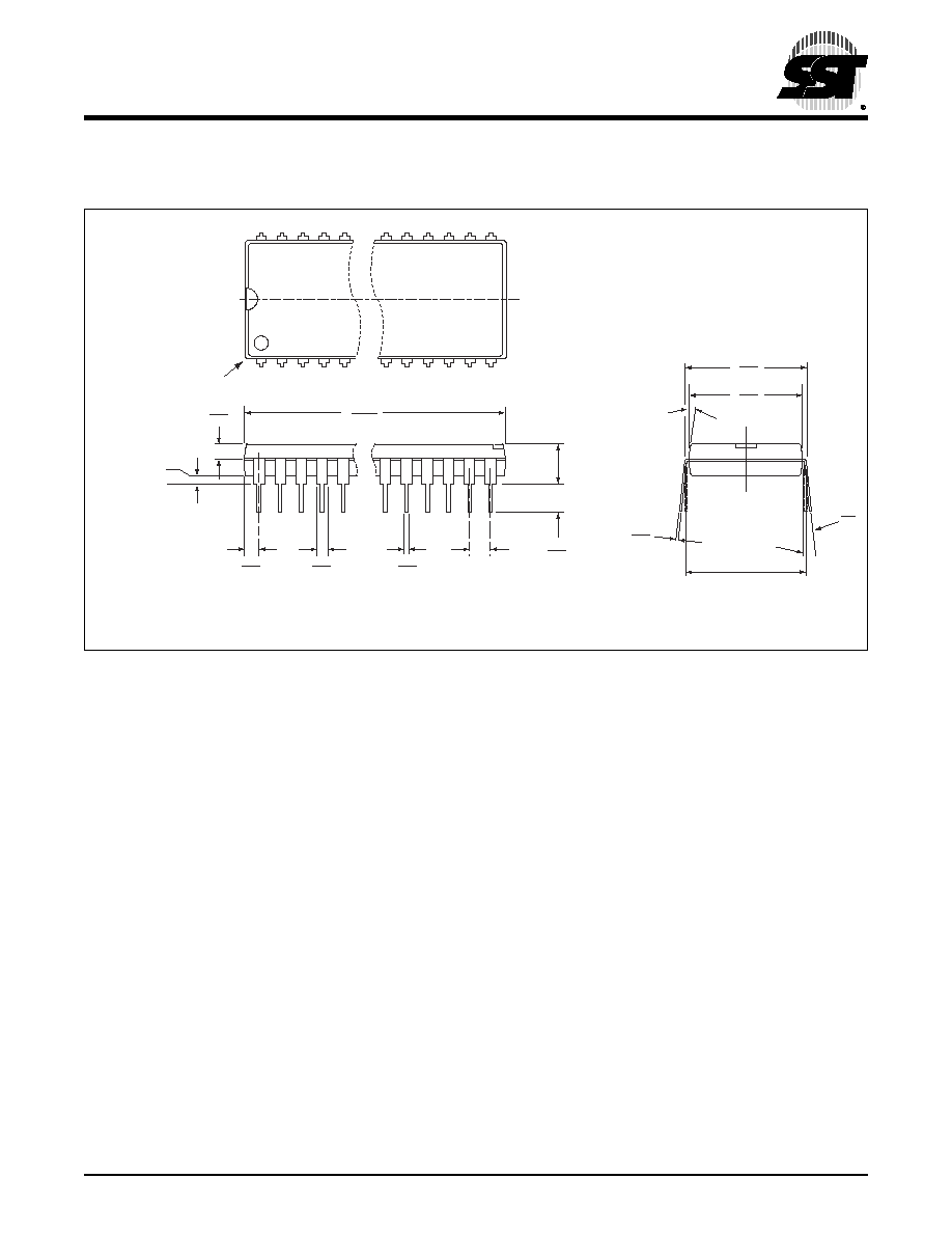
Preliminary Specifications
FlashFlex51 MCU
SST89E52RD2 / SST89E54RD2 / SST89E58RD2 / SST89E516RD2
SST89V52RD2 / SST89V54RD2 / SST89V58RD2 / SST89V516RD2
89
©2004 Silicon Storage Technology, Inc.
S71255-00-000
3/04
16.0 PACKAGING DIAGRAMS
40-
PIN
P
LASTIC
D
UAL
I
N
-
LINE
P
INS
(PDIP)
SST P
ACKAGE
C
ODE
: PI
40-pdip-PI-7
Pin #1 Identifier
CL
40
1
Base Plane
Seating Plane
.220 Max.
12∞
4 places
.600 BSC
.100 BSC
.100
.200
.015
.022
.045
.055
.063
.090
.015 Min.
.065
.075
2.020
2.070
.008
.012
0∞
15∞
.600
.625
.530
.557
Note:
1. Complies with JEDEC publication 95 MS-011 AC dimensions (except as noted), although some dimensions may be more stringent.
= JEDEC min is .115; SST min is
less stringent
2. All linear dimensions are in inches (min/max).
3. Dimensions do not include mold flash. Maximum allowable mold flash is .010 inches.

90
Preliminary Specifications
FlashFlex51 MCU
SST89E52RD2 / SST89E54RD2 / SST89E58RD2 / SST89E516RD2
SST89V52RD2 / SST89V54RD2 / SST89V58RD2 / SST89V516RD2
©2004 Silicon Storage Technology, Inc.
S71255-00-000
3/04
44-
LEAD
P
LASTIC
L
EAD
C
HIP
C
ARRIER
(PLCC)
SST P
ACKAGE
C
ODE
: NJ
.025
.045
.013
.021
.590
.630
.100
.112
.020 Min.
.165
.180
TOP VIEW
SIDE VIEW
BOTTOM VIEW
1
44
.026
.032
.500
REF.
44-plcc-NJ-7
Note:
1. Complies with JEDEC publication 95 MS-018 AC dimensions (except as noted), although some dimensions may be more stringent.
= JEDEC min is .650; SST min is
less stringent
2. All linear dimensions are in inches (min/max).
3. Dimensions do not include mold flash. Maximum allowable mold flash is .008 inches.
4. Coplanarity: 4 mils.
.050
BSC.
.050
BSC.
.026
.032
.042
.056
.646
.656
.042
.048
.042
.048
Optional
Pin #1 Identifier
.646
.656
.685
.695
.685
.695
.020 R.
MAX.
.147
.158
R.
x45∞

Preliminary Specifications
FlashFlex51 MCU
SST89E52RD2 / SST89E54RD2 / SST89E58RD2 / SST89E516RD2
SST89V52RD2 / SST89V54RD2 / SST89V58RD2 / SST89V516RD2
91
©2004 Silicon Storage Technology, Inc.
S71255-00-000
3/04
44-
LEAD
T
HIN
Q
UAD
F
LAT
P
ACK
(TQFP)
SST P
ACKAGE
C
ODE
: TQJ
TABLE
16-1: R
EVISION
H
ISTORY
Number
Description
Date
00
∑
Initial Release
Mar 2004
Note:
1. Complies with JEDEC publication 95 MS-026 ACB dimensions, although some dimensions may be more stringent.
2. All linear dimensions are in millimeters (min/max).
3. Coplanarity: 0.1 (±0.05) mm.
4. Package body dimensions do not include mold flash. Maximum allowable mold flash is .25mm.
44-tqfp-TQJ-7
.45
.75
10.00 ± 0.10
12.00 ± 0.25
1.00 ref
0∞- 7∞
1
11
33
23
12
22
44
34
1.2
max.
.95
1.05
.05
.15
Pin #1 Identifier
.30
.45
.09
.20
.80 BSC
12.00 ± 0.25
10.00 ± 0.10
1mm
Silicon Storage Technology, Inc. ∑ 1171 Sonora Court ∑ Sunnyvale, CA 94086 ∑ Telephone 408-735-9110 ∑ Fax 408-735-9036
www.SuperFlash.com or www.sst.com