 | –≠–ª–µ–∫—Ç—Ä–æ–Ω–Ω—ã–π –∫–æ–º–ø–æ–Ω–µ–Ω—Ç: SPA-2318 | –°–∫–∞—á–∞—Ç—å:  PDF PDF  ZIP ZIP |
The information provided herein is believed to be reliable at press time. Stanford Microdevices assumes no responsibility for inaccuracies or omissions.
Stanford Microdevices assumes no responsibility for the use of this information, and all such information shall be entirely at the user's own risk. Prices and specifications are
subject to change without notice. No patent rights or licenses to any of the circuits described herein are implied or granted to any third party. Stanford Microdevices does not
authorize or warrant any Stanford Microdevices product for use in life-support devices and/or systems.
Copyright 2001 Stanford Microdevices, Inc. All worldwide rights reserved.
1
Product Description
Preliminary
EDS-101432 Rev B
Phone: (800) SMI-MMIC
http://www.stanfordmicro.com
726 Palomar Ave., Sunnyvale, CA 94085
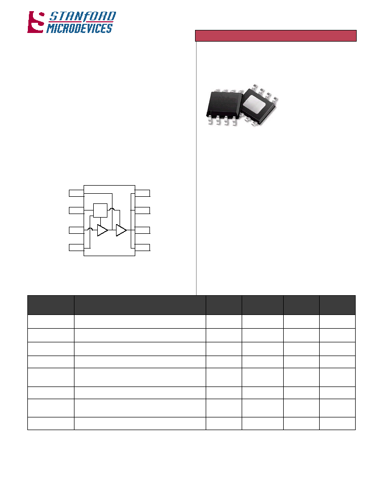
SPA-2318
2150 MHz 1 Watt Power Amplifier
with Active Bias
Product Features
∑
High Linearity Performance:
+47 dBm Typ. OIP3 at 2140 MHz
+21.7 dBm W-CDMA Channel Power
at -45 dBc ACP
∑
On-chip Active Bias Control
∑
High Gain: 23 dB Typ.
∑
Patented High Reliability GaAsHBT Technology
∑
Surface-Mountable Plastic Package
Applications
∑
W-CDMA Systems
∑
Multi-Carrier Applications
Stanford Microdevices' SPA-2318 is a high efficiency GaAs
Heterojunction Bipolar Transistor (HBT) amplifier housed in
a low-cost surface-mountable plastic package. These HBT
amplifiers are fabricated using molecular beam epitaxial
growth technology which produces reliable and consistent
performance from wafer to wafer and lot to lot.
This product is specifically designed for use as a driver
amplifier for infrastructure equipment in the 2150 MHz PCS
band. Its high linearity makes it an ideal choice for multi-carrier
and digital applications.
l
o
b
m
y
S
:
s
n
o
i
t
i
d
n
o
C
t
s
e
T
:
s
r
e
t
e
m
a
r
a
P
Z
0
5
2
=
p
m
e
T
s
m
h
O
0
5
=
∫
V
0
.
5
=
c
c
V
,
C
s
t
i
n
U
.
n
i
M
.
p
y
T
.
x
a
M
f
0
n
o
it
a
r
e
p
O
f
o
y
c
n
e
u
q
e
r
F
z
H
M
0
1
1
2
0
4
1
2
0
7
1
2
P
B
d
1
n
o
i
s
s
e
r
p
m
o
C
B
d
1
t
a
r
e
w
o
P
t
u
p
t
u
O
m
B
d
8
2
S
1
2
n
i
a
G
l
a
n
g
i
S
ll
a
m
S
B
d
3
2
R
W
S
V
R
W
S
V
t
u
p
n
I
-
1
:
5
.
1
P
I
O
3
t
n
i
o
P
t
p
e
c
r
e
t
n
I
r
e
d
r
O
d
r
i
h
T
t
u
p
t
u
O
m
B
d
4
1
+
=
e
n
o
t
r
e
p
t
u
o
r
e
w
o
P
m
B
d
7
4
F
N
e
r
u
g
i
F
e
s
i
o
N
B
d
0
.
5
c
c
I
t
n
e
r
r
u
C
e
c
i
v
e
D
s
a
i
b
I
,
A
m
0
1
=
1
c
I
,
A
m
0
7
=
2
c
I
A
m
0
2
3
=
A
m
0
0
4
R
l-
j
h
t
)
d
a
e
l
-
n
o
it
c
n
u
j(
e
c
n
a
t
s
i
s
e
R
l
a
m
r
e
h
T
W
/
C
∫
2
3
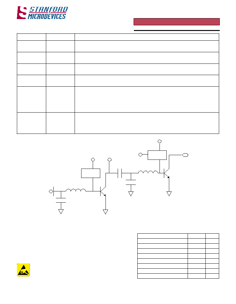
VC1
VBIAS
RFIN
VPC2
RFOUT/
VC2
Active
Bias
2
Preliminary
Preliminary
SPA-2318 2150 MHz 1 Watt Power Amp
EDS-101432 Rev B
Phone: (800) SMI-MMIC
http://www.stanfordmicro.com
726 Palomar Ave., Sunnyvale, CA 94085
24
26
28
30
2.11
2.12
2.13
2.14
2.15
2.16
2.17
25C
85C
-40C
15
18
21
24
27
30
2.11
2.12
2.13
2.14
2.15
2.16
2.17
25C
-40C
85C
-40
-34
-28
-22
-16
-10
-4
2.11
2.12
2.13
2.14
2.15
2.16
2.17
40
42
44
46
48
50
52
2.11
2.12
2.13
2.14
2.15
2.16
2.17
25C
85C
-40C
38
40
42
44
46
48
50
52
10
12
14
16
18
20
25C
85C
-40C
0
100
200
300
400
500
600
0
1
2
3
4
5
6
25C
-40C
85C
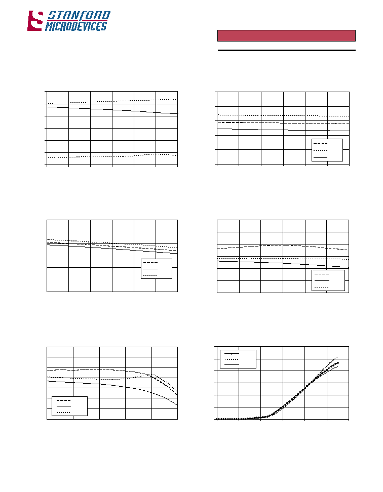
P1dB vs Frequency
GHz
dBm
2140 MHz Application Circuit Data, Icc=400mA, T=+25C, Vcc=5V
Note: Tuned for Output IP3
Input/Output Return Loss,
Isolation vs Frequency
GHz
dB
S11
S22
GHz
Gain vs. Frequency
dB
Output Third Order Intercept vs. Frequency
(P
OUT
per tone = 14dBm)
GHz
dBm
Output Third Order Intercept vs. Tone Power
2.14GHz
P
OUT
per tone (dBm)
dBm
S12
Device Current vs. Source Voltage
V
cc
(V)
Device Current (mA)
Preliminary
Preliminary
SPA-2318 2150 MHz 1 Watt Power Amp
3
EDS-101432 Rev B
Phone: (800) SMI-MMIC
http://www.stanfordmicro.com
726 Palomar Ave., Sunnyvale, CA 94085
-65
-60
-55
-50
-45
-40
-35
-30
19
20
21
22
23
24
25
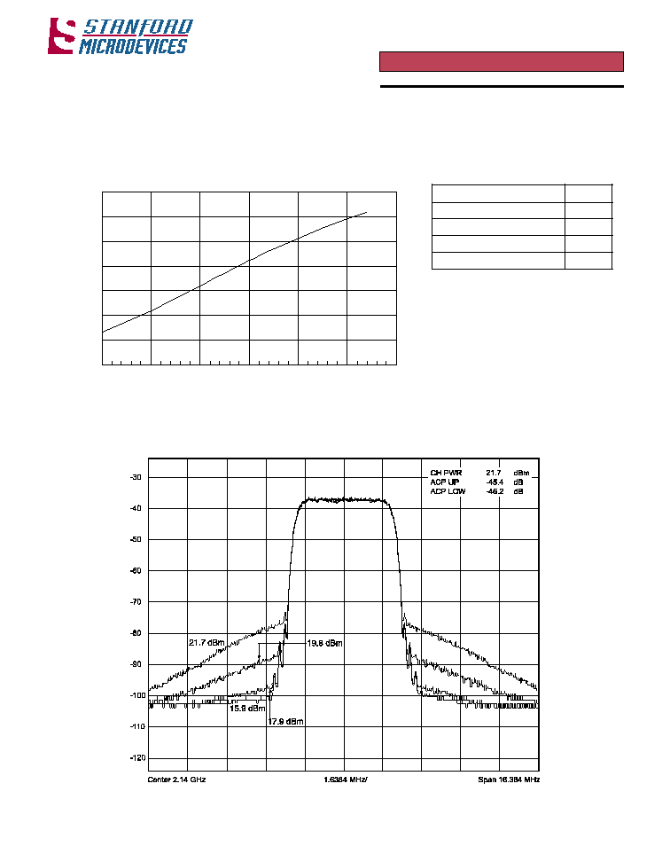
W-CDMA at 2.14 GHz
Channel Output Power (dBm)
Adjacent Channel Power (dBc)
W-CDMA at 2.14 GHz Adjacent Channel Power
vs. Channel Output Power
2140 MHz Application Circuit Data, Icc=400mA, T=+25C, Vcc=5V
*Note: IP3 performance degraded due to Device
being tuned for optimal ACP performance
y
c
n
e
u
q
e
r
F
0
4
1
2
z
H
M
)
B
d
(
n
i
a
G
l
a
n
g
i
S
ll
a
m
S
4
.
3
2
P
C
A
c
B
d
5
4
-
@
)
m
B
d
(
.r
w
P
.
h
C
7
.
1
2
)
m
B
d
(
3
P
I
t
u
p
t
u
O
*
4
.
5
4
)
m
B
d
(
B
d
1
P
9
.
9
2
The W-CDMA setup is PCCPCH+PSCH+SSCH+CPICH+PICH+64 DPCH
4
Preliminary
Preliminary
SPA-2318 2150 MHz 1 Watt Power Amp
EDS-101432 Rev B
Phone: (800) SMI-MMIC
http://www.stanfordmicro.com
726 Palomar Ave., Sunnyvale, CA 94085
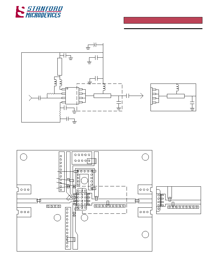
Vcc
1.8pF
18 nH
5.6pF
10uF Tantalum
39pF
1.5pF
2.7nH
1000pF
56pF
5.6nH
6.8K
300 ohm 1800pF
.1uF Tantalum
Note: All inductors are Toko LL1608-FS
Z=
63
, 2
3
.5
∞
5
6
7
8
4
3
2
1
Z=50
, 27.4 ∞
1.8pF
18 nH
5
6
7
8
Z=50
, 13.1 ∞
Tune for optimal ACP performance
Tune for optimal IP3 performance
2110 - 2170 MHz Schematic
2110 - 2170 MHz Evaluation Board Layout
Vpc
Vbias
Eval Board
ECB-101161 Rev. B
SOIC-8 PA
Vcc
39pF
1.5pF
5.6nH
Short
18nH
1800pF
5.6pF
56pF
1.8pF
2.7nH
1000pF
10uF Tantalum
.1uF
Tantalum
Note: All inductors are
Toko LL1608-FS
6.8K
300
18nH
1.8pF
Tune for optimal ACP performance
Tune for optimal IP3 performance
Preliminary
Preliminary
SPA-2318 2150 MHz 1 Watt Power Amp
5
EDS-101432 Rev B
Phone: (800) SMI-MMIC
http://www.stanfordmicro.com
726 Palomar Ave., Sunnyvale, CA 94085
#
n
i
P
n
o
i
t
c
n
u
F
n
o
i
t
p
i
r
c
s
e
D
1
1
C
V
s
a
n
o
it
a
r
u
g
if
n
o
c
e
h
T
.r
o
t
s
i
s
n
a
r
t
e
g
a
t
s
t
s
r
if
e
h
t
r
o
f
e
g
a
tl
o
v
y
l
p
p
u
s
e
h
t
s
i
1
C
V
.
e
c
n
a
m
r
o
f
r
e
p
F
R
m
u
m
it
p
o
r
o
f
d
e
r
i
u
q
e
r
s
i
c
it
a
m
e
h
c
s
n
o
it
a
c
il
p
p
a
n
o
n
w
o
h
s
2
s
a
i
b
V
d
e
d
n
e
m
m
o
c
e
R
.
k
r
o
w
t
e
n
s
a
i
b
e
v
it
c
a
e
h
t
r
o
f
n
i
p
l
o
r
t
n
o
c
s
a
i
b
e
h
t
s
i
s
a
i
b
V
.
c
it
a
m
e
h
c
S
n
o
it
a
c
il
p
p
A
e
h
t
n
i
n
w
o
h
s
s
i
n
o
it
a
r
u
g
if
n
o
c
3
n
I
F
R
s
a
r
o
ti
c
a
p
a
c
g
n
i
k
c
o
l
b
C
D
l
a
n
r
e
t
x
e
n
a
f
o
e
s
u
e
h
t
s
e
r
i
u
q
e
r
n
i
p
s
i
h
T
.
n
i
p
t
u
p
n
i
F
R
.
c
it
a
m
e
h
c
S
n
o
it
a
c
il
p
p
A
e
h
t
n
i
n
w
o
h
s
4
2
C
P
V
.
e
g
a
t
s
d
n
o
c
e
s
e
h
t
r
o
f
k
r
o
w
t
e
n
s
a
i
b
e
v
it
c
a
e
h
t
r
o
f
n
i
p
l
o
r
t
n
o
c
s
a
i
b
e
h
t
s
i
2
C
P
V
.
c
it
a
m
e
h
c
S
n
o
it
a
c
il
p
p
A
e
h
t
n
i
n
w
o
h
s
s
i
n
o
it
a
r
u
g
if
n
o
c
d
e
d
n
e
m
m
o
c
e
r
e
h
T
8
,
7
,
6
,
5
2
C
V
/t
u
O
F
R
l
a
n
r
e
t
x
e
n
a
h
g
u
o
r
h
t
n
i
p
s
i
h
t
o
t
d
e
il
p
p
u
s
e
b
d
l
u
o
h
s
s
a
i
B
.
n
i
p
s
a
i
b
d
n
a
t
u
p
t
u
o
F
R
r
o
ti
c
a
p
a
c
g
n
i
k
c
o
l
b
C
D
a
,
n
i
p
s
i
h
t
n
o
t
n
e
s
e
r
p
s
i
g
n
i
s
a
i
b
C
D
e
s
u
a
c
e
B
.
e
k
o
h
c
F
R
y
l
p
p
u
s
e
h
T
.
)
c
it
a
m
e
h
c
s
n
o
it
a
c
il
p
p
a
e
e
s
(
s
n
o
it
a
c
il
p
p
a
t
s
o
m
n
i
d
e
s
u
e
b
d
l
u
o
h
s
s
i
k
r
o
w
t
e
n
g
n
i
h
c
t
a
m
t
u
p
t
u
o
n
A
.
d
e
s
s
a
p
y
b
ll
e
w
e
b
d
l
u
o
h
s
k
r
o
w
t
e
n
s
a
i
b
e
h
t
f
o
e
d
i
s
.
e
c
n
a
m
r
o
f
r
e
p
m
u
m
it
p
o
r
o
f
y
r
a
s
s
e
c
e
n
D
A
P
E
d
n
G
e
h
t
o
t
d
e
r
e
d
l
o
s
e
b
o
t
s
d
e
e
n
e
g
a
k
c
a
p
e
h
t
f
o
e
d
i
s
m
o
tt
o
b
e
h
t
n
o
a
e
r
a
d
e
s
o
p
x
E
l
a
r
e
v
e
S
.
e
c
n
a
m
r
o
f
r
e
p
F
R
d
n
a
l
a
m
r
e
h
t
m
u
m
it
p
o
r
o
f
d
r
a
o
b
e
h
t
f
o
e
n
a
l
p
d
n
u
o
r
g
d
n
a
l
d
e
d
n
e
m
m
o
c
e
r
e
h
t
n
i
n
w
o
h
s
s
a
D
A
P
E
e
h
t
r
e
d
n
u
d
e
t
a
c
o
l
e
b
d
l
u
o
h
s
s
a
i
v
.
)
6
e
g
a
p
(
n
r
e
tt
a
p
2
3
5-8
ACTIVE BIAS
NETW ORK
ACTIVE BIAS
NETW ORK
2
4
1
Simplified Device Schematic
Absolute Maximum Ratings
r
e
t
e
m
a
r
a
P
e
u
l
a
V
t
i
n
U
V
(
t
n
e
r
r
u
C
y
l
p
p
u
S
1
C
)
0
5
1
A
m
V
(
t
n
e
r
r
u
C
y
l
p
p
u
S
2
C
)
0
5
7
A
m
V
(
e
g
a
tl
o
V
e
c
i
v
e
D
D
)
0
.
6
V
n
o
it
a
p
i
s
s
i
D
r
e
w
o
P
0
.
4
W
T
(
e
r
u
t
a
r
e
p
m
e
T
d
a
e
L
g
n
it
a
r
e
p
O
L
)
5
8
+
o
t
0
4
-
C
∫
r
e
w
o
P
t
u
p
n
I
F
R
0
4
+
W
m
e
g
n
a
R
e
r
u
t
a
r
e
p
m
e
T
e
g
a
r
o
t
S
0
5
1
+
o
t
0
4
-
C
∫
T
(
e
r
u
t
a
r
e
p
m
e
T
n
o
it
c
n
u
J
g
n
it
a
r
e
p
O
J
)
0
5
1
+
C
∫
Operation of this device above any one of these
parameters may cause permanent damage.
Bias Conditions should also satisfy the following
expression: I
D
V
D
(max) < (T
J
- T
L
)/R
th,j-l
Caution: ESD sensitive
Appropriate precautions in handling, packaging and
testing devices must be observed.