The information provided herein is believed to be reliable at press time. Stanford Microdevices assumes no responsibility for inaccuracies or ommisions.
Stanford Microdevices assumes no responsibility for the use of this information, and all such information shall be entirely at the user's own risk. Prices and specifications are subject to change without
notice. No patent rights or licenses to any of the circuits described herein are implied or granted to any third party. Stanford Microdevices does not authorize or warrant any Stanford Microdevices
product for use in life-support devices and/or systems.
Copyright 2000 Stanford Microdevices, Inc. All worldwide rights reserved.
522 Almanor Ave., Sunnyvale, CA 94086
Phone: (800) SMI-MMIC
http://www.stanfordmicro.com
1
05/04/01 rev 1.0
Advanced Data Sheet
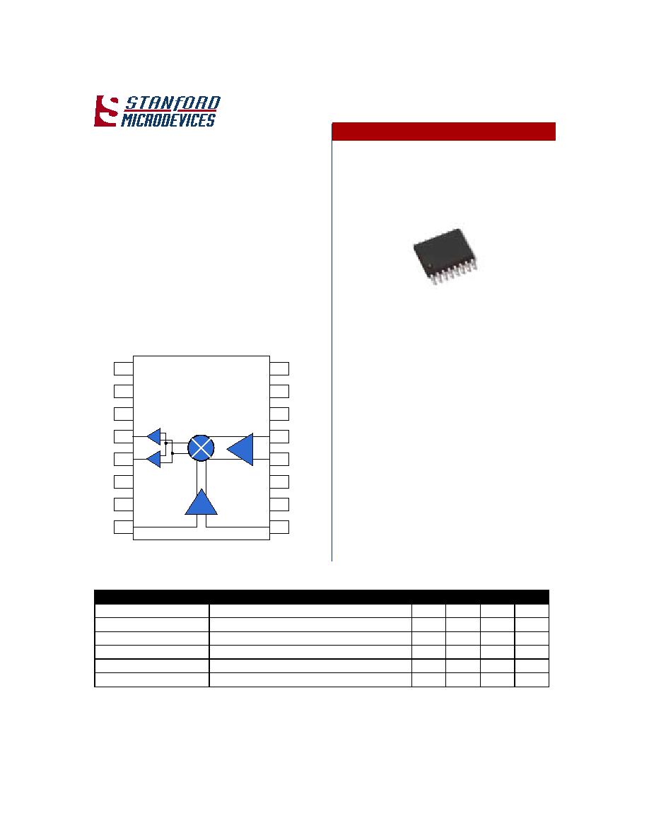
The Stanford Microdevices' STM-2016 is a high linearity
active mixer for use in a wide variety of communication
systems covering the 1800-2200 MHz frequency bands.
This device operates from a single 5V supply and provides
9dB of conversion gain while requiring only 0dBm input to
the integrated LO driver. The STM-2016 also includes an
integrated on chip IF amplifier and is fabricated using sili-
con germanium device technology.
The STM-2016 incorporates internal matching on each RF,
IF, and LO port to enhance ease of use and to reduce the
number of external components required. The IF and LO
ports can be driven differential or single ended. Each
broadband port has been designed to minimize perfor-
mance degradation while operating into highly reactive
components such as SAW filters.
Key Specifications
Parameters
Test Conditions (V
CC
=5.0V, I=190mA, T=25�C)
Unit
Min.
Typ.
Max.
RF Frequency Range
MHz
1800
2200
IF Frequency Range
MHz
10
200
300
Output IP3
IF1 = IF2 = -20 dBm/tone
dBm
+15
Output P1dB
dBm
+3.5
Conversion Gain
dB
9
SSB Noise Figure
dB
9
Functional Block Diagram
STM-2016
1800 - 2200 MHz High Linearity
Silicon Germanium
Active Transmit Mixer
Product Features
Applications
�
Active mixer with conversion gain
�
No need for separate external LO driver
�
Low LO drive level required to drive mixer
�
IF and LO ports may be driven single-ended
�
Single supply operation (+5V)
�
Broadband resistive 50
impedances on all
three ports
�
Digital and spread spectrum communication
systems
�
1800-2200 MHz transceivers for base station
infrastructure equipment
Product Description
16 pin TSSOP with Exposed Pad
Package Body: 0.20 x 0.17 x 0.04 (inches)
5.0 x 4.4 x 1.0 (mm)
1
2
3
4
5
6
7
8
16
15
14
13
12
11
10
9
LOP
LON
VEE
VEE
RFP
RFN
VCC
VEE
VEE
VCC
IFN
VCC
VEE
VEE
VCC
IFP
The information provided herein is believed to be reliable at press time. Stanford Microdevices assumes no responsibility for inaccuracies or ommisions.
Stanford Microdevices assumes no responsibility for the use of this information, and all such information shall be entirely at the user's own risk. Prices and specifications are subject to change without
notice. No patent rights or licenses to any of the circuits described herein are implied or granted to any third party. Stanford Microdevices does not authorize or warrant any Stanford Microdevices
product for use in life-support devices and/or systems.
Copyright 2000 Stanford Microdevices, Inc. All worldwide rights reserved.
522 Almanor Ave., Sunnyvale, CA 94086
Phone: (800) SMI-MMIC
http://www.stanfordmicro.com
2
05/04/01 rev 1.0
Advanced Data Sheet
670 0+] 7UDQVPLW 0L[HU
Absolute Maximum Ratings
Parameters
Value
Unit
Supply Voltage
+6.0
V
DC
LO Input
+10
dBm
RF Input
+15
dBm
Operating Temperature
-40 to +85
�C
Storage Temperature
-65 to +150
�C
Test Conditions
VCC
+5.0V
TA
+25�C
IF Input
-20 dBm @ 200 MHz
LO Input
0 dBm @ 1760 MHz
Product Specifications � AC Performance
Parameters
Additional Test Conditions
Unit
Min.
Typ.
Max.
RF Frequency Range
MHz
1800
2200
IF Frequency Range
MHz
10
200
300
Output IP3
IF1 = IF2 = -20 dBm/tone
dBm
+15
Output P1dB
dBm
+3.5
Conversion Gain
dB
9
SSB Noise figure
dB
9
RF Return Loss
dB
14
LO Return Loss
dB
14
IF Return Loss
dB
14
LO Drive
dBm
-3
0
+3
Product Specifications � Miscellaneous
Parameters
Additional Test Conditions
Unit
Min.
Typ.
Max.
Supply Voltage
V
+4.75
+5.0
+5.25
Supply Current
mA
190
Thermal Resistance
�C/W
TBD
Product Specifications � Isolation Performance
Parameters
Additional Test Conditions
Unit
Min.
Typ.
Max.
Leakage (LO-RF)
dBm
-25
Leakage (LO-IF)
dBm
-30
The information provided herein is believed to be reliable at press time. Stanford Microdevices assumes no responsibility for inaccuracies or ommisions.
Stanford Microdevices assumes no responsibility for the use of this information, and all such information shall be entirely at the user's own risk. Prices and specifications are subject to change without
notice. No patent rights or licenses to any of the circuits described herein are implied or granted to any third party. Stanford Microdevices does not authorize or warrant any Stanford Microdevices
product for use in life-support devices and/or systems.
Copyright 2000 Stanford Microdevices, Inc. All worldwide rights reserved.
522 Almanor Ave., Sunnyvale, CA 94086
Phone: (800) SMI-MMIC
http://www.stanfordmicro.com
3
05/04/01 rev 1.0
Advanced Data Sheet
670 0+] 7UDQVPLW 0L[HU
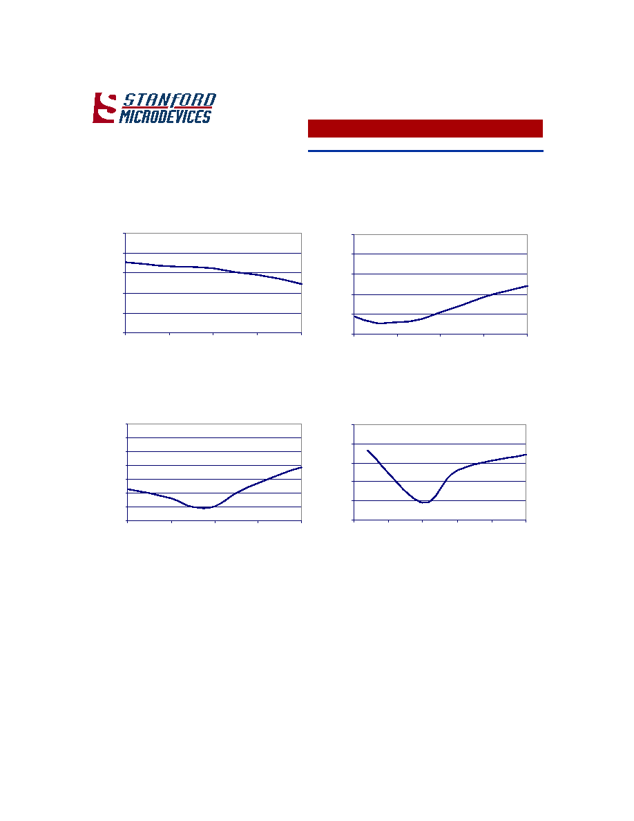
Typical Device Performance
Conversion Gain
V
CC
= 5.0V, RF = 1.96GHz, IF = 200MHz
2
4
6
8
10
12
1.8
1.9
2.0
2.1
2.2
RF Frequency (GHz)
Ga
in
(d
B)
Return Loss at LO Input
V
CC
= 5.0V
-35
-30
-25
-20
-15
-10
-5
0
1.6
1.7
1.8
1.9
2.0
LO Frequency (GHz)
Re
tu
r
n
L
o
s
s
(d
B)
Return Loss at IF Input
V
CC
= 5.0V
-50
-40
-30
-20
-10
0
50
100
150
200
250
300
IF Frequency (MHz)
Re
tu
r
n
L
o
s
s
(d
B)
Return Loss at RF Input
V
CC
= 5.0V
-25
-20
-15
-10
-5
0
1.8
1.9
2.0
2.1
2.2
RF Fre quency (GHz)
Re
tu
r
n
L
o
s
s
(d
B)
NOTE: The data shown in the graphs above demonstrates the STM-2016 performance tuned to the PCS band.

The information provided herein is believed to be reliable at press time. Stanford Microdevices assumes no responsibility for inaccuracies or ommisions.
Stanford Microdevices assumes no responsibility for the use of this information, and all such information shall be entirely at the user's own risk. Prices and specifications are subject to change without
notice. No patent rights or licenses to any of the circuits described herein are implied or granted to any third party. Stanford Microdevices does not authorize or warrant any Stanford Microdevices
product for use in life-support devices and/or systems.
Copyright 2000 Stanford Microdevices, Inc. All worldwide rights reserved.
522 Almanor Ave., Sunnyvale, CA 94086
Phone: (800) SMI-MMIC
http://www.stanfordmicro.com
4
05/04/01 rev 1.0
Advanced Data Sheet
670 0+] 7UDQVPLW 0L[HU
Pin Out Description
Pin #
Function
Description
Additional Comments
1
VEE
Ground
2
VCC
Positive supply (+5V)
3
VEE
Ground
4
RFN
RF input, negative terminal
Nominal DC voltage is 2.3V. (Internally biased) Output should be
AC-coupled.
5
RFP
RF input, positive terminal
Nominal DC voltage is 2.3V. (Internally biased) Output should be
AC-coupled.
6
VEE
Ground
7
VCC
Positive supply (+5V)
8
IFN
IF output, negative terminal
Nominal DC voltage is 2.2V. (Internally biased) Input should be AC-
coupled
9
IFP
IF output, positive terminal
Nominal DC voltage is 2.2V. (Internally biased) Input should be AC-
coupled
10
VCC
Positive supply (+5V)
11
VEE
Ground
12
LOP
LO input, positive terminal
Nominal DC voltage is 2.3V. (Internally biased) Input should be AC-
coupled.
13
LON
LO input, negative terminal
Nominal DC voltage is 2.3V. (Internally biased) Input should be AC-
coupled.
14
VEE
Ground
15
VCC
Positive supply (+5V)
16
VEE
Ground
The information provided herein is believed to be reliable at press time. Stanford Microdevices assumes no responsibility for inaccuracies or ommisions.
Stanford Microdevices assumes no responsibility for the use of this information, and all such information shall be entirely at the user's own risk. Prices and specifications are subject to change without
notice. No patent rights or licenses to any of the circuits described herein are implied or granted to any third party. Stanford Microdevices does not authorize or warrant any Stanford Microdevices
product for use in life-support devices and/or systems.
Copyright 2000 Stanford Microdevices, Inc. All worldwide rights reserved.
522 Almanor Ave., Sunnyvale, CA 94086
Phone: (800) SMI-MMIC
http://www.stanfordmicro.com
5
05/04/01 rev 1.0
Advanced Data Sheet
670 0+] 7UDQVPLW 0L[HU
Part Number Ordering Information
Part Number
Reel Size
Devices/Reel
STM-2016
TBD
TBD
Caution: ESD Sensitive
Appropriate precaution in handling, packaging
and testing devices must be observed.
Part Symbolization
The part will be symbolized with a "TBD" marking
designator on the top surface of the package.
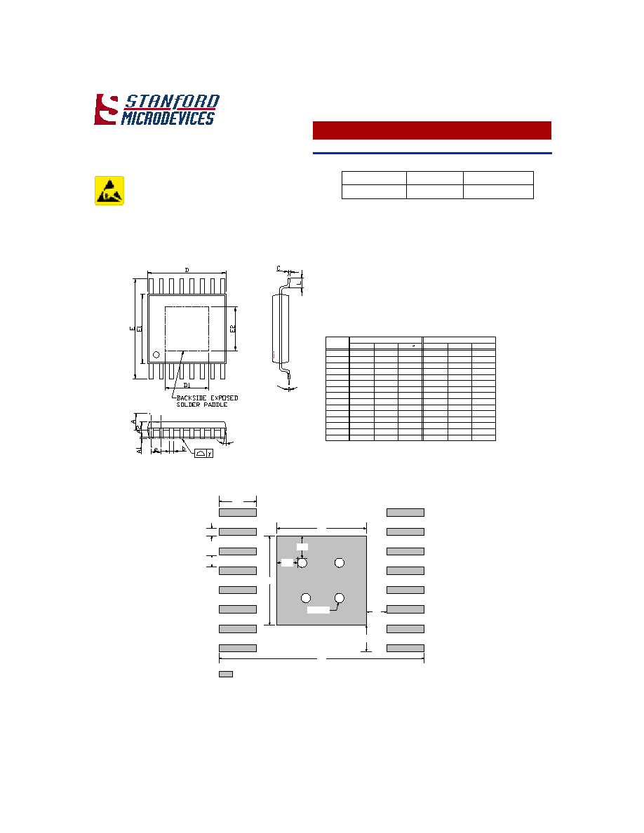
Package Dimensions ("16" Package)
Test PCB Pad Layout
12�(4X)
NOTE
1. PACKAGE BODY SIZES EXCLUDE MOLD FLASH
PROTRUSIONS OR GATE BURRS
2. TOLERANCE �0.1 mm UNLESS OTHERWISE SPECIFIED
3. COPLANARITY : 0.1 mm
4. CONTROLLING DIMENSION IS MILLIMETER. CONVERTED
INCH DIMENSIONS ARE NOT NECESSARILY EXACT.
5. FOLLOWED FROM JEDEC MO-153
0.030
0.024
0.60
0.75
0.45
L
0.018
0�
---
y
0�
---
8�
0.10
---
---
---
---
8�
0.004
MIN
---
0.000
0.031
---
0.193
0.004
---
0.169
0.007
DIMENSIONS IN MILLIMETERS
0.00
A1
D
E1
e
E
b
C
A2
4.90
---
4.30
---
0.80
0.09
0.19
SYMBOLS
A
---
MIN
---
0.10
1.05
5.10
---
0.20
4.50
---
0.30
5.00
4.40
0.65
6.40
---
---
1.00
MAX
1.15
---
NOM
0.004
---
0.197
0.173
0.026
0.252
0.039
---
---
0.201
---
0.177
---
0.041
0.008
0.012
DIMENSIONS IN INCHES
NOM
---
0.045
MAX
D1
2.80
0.110
---
---
---
---
E2
2.80
0.110
---
---
---
---
3.0
3.0
0.25
1.25
6.9
0.74
0.74
0.7
0.9
0.4
0.33 via
- Indicates metalization
- vias connect pad to underlying ground plane
all units are in mm