11
SMT SHAPE - INFRARED LED
n
Infrared LED
Unit
nm
mA
mW/sr
mA
mW
mA
MHz
mA
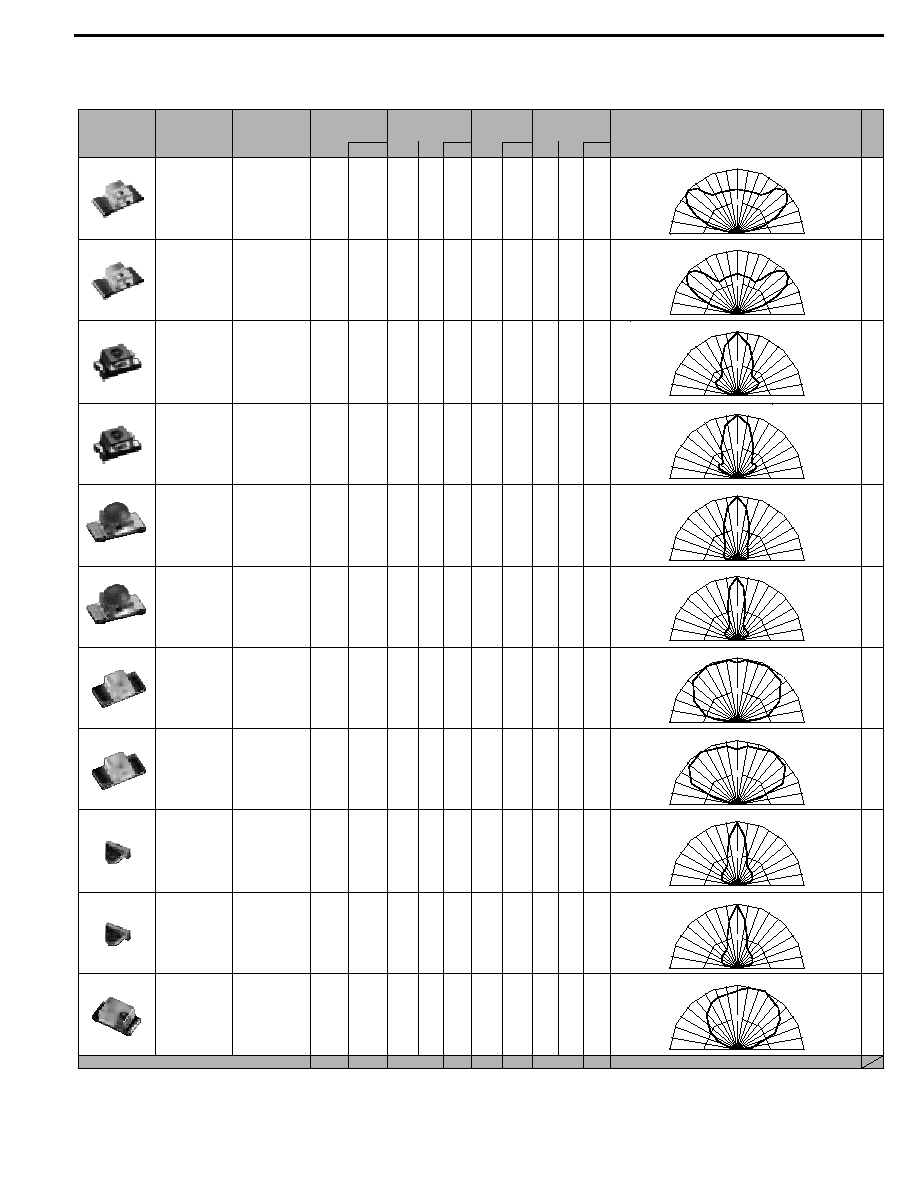
Part No.
Features
Peak
Wavelength
l
P
Cut-Off Frequency
Fc
Output Power
Po
I
F
Spatial Distribution
(The typical distribution example of
each shape is shown below)
TYP.
I
F
TYP.
Shape
fig.
MIN.
1
F
TYP.
MIN.
Radiant Intensity
I
E
I
F
TYP.
DNP1101W
AN1101W
DNP1102W
AN1102W
DNP1105W
AN1105W
DNP1111R
AN1111R
DNP1102F
AN1102F
AN1111C
Flat lens
package
Flat lens
package
Inner lens
package
Inner lens
package
Dome-lens
High radiant
intensity
Reverse and
standard
mounting
Dome-lens
High radiant
intensity
Reverse and
standard
mounting
Reverse mount
Flat lens
package
Reverse mount
Flat lens
package
Side view
package
Side view
package
Compact
1608 size
880
950
880
950
880
950
880
950
880
950
950
20
20
20
20
20
20
20
20
50
20
20
0.5
0.2
--
0.5
2.0
1.0
0.5
0.2
1.5
0.35
0.2
1.0
0.4
2.2
0.8
4.0
1.4
1.0
0.28
3.0
0.5
0.28
20
20
20
20
20
20
20
20
20
20
20
5
2
4
2
2
2
5
2
2
2
2
20
20
20
20
20
20
20
20
20
20
20
--
--
--
--
--
--
--
--
--
--
--
12
0.5
12
0.5
12
0.5
12
0.5
12
0.5
0.5
20
20
20
20
20
20
20
20
20
20
20
60
0
30
60
90
90
30
0.5
60
0
30
60
90
90
30
0.5
60
0
30
60
90
90
30
0.5
60
0
30
60
90
90
30
0.5
60
0
30
60
90
90
30
0.5
60
0
30
60
90
90
30
0.5
60
0
30
60
90
90
30
0.5
60
0
30
60
90
90
30
0.5
60
0
30
60
90
90
30
0.5
60
0
30
60
90
90
30
0.5
60
0
30
60
90
90
30
0.5
Ta=25∞C
1
1
2
2
3
3
4
5
6
6
7
v
All above products contain no lead
12
SMT SHAPE - INFRARED LED
n
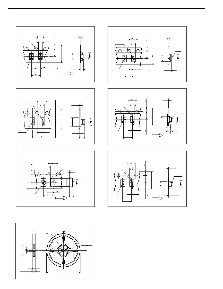
Package Dimensions
unit: mm
3
1.5
0.9
2
1.5
1.6
(4.4)
(1.6)
0.6
1.3
(1.6)
2
Cathode Mark
1
Tolerance:
±
0.2
fig. 1
3
1.5
1
2
Lens
0.9
2
1.8
0.6
Cathode Mark
1.6
1
2
1.3
(1.6)
(1.6)
(4.4)
1
2
Tolerance:
±
0.2
fig. 2
1
1
2
1
2
2
3.2
0.6
1.6
(1.6)
(1.6)
2.3
(2)
2.1
1.5
1.5
(4.6)
0.5
0.5
1.6
1.55
0.3
R0.8
Cathode Mark
Polarity Mark
Hole
PCB
PCB
Tolerance:
±
0.1
fig. 3
1.4
0.8
0.3
0.1
1.4
3.2
0.75
1.6
(1.6)
(1.5)
(2.3)
(2.1)
Hole
PCB
Cathode Mark
0.5
0.5
Pin Connection
Mark
1
2
1
2
(1.5)
1
2
Tolerance:
±
0.1
fig. 4
Recommended Soldering Pattern
Standard Mount
Recommended Soldering Pattern
Recommended Soldering Pattern
Recommended Soldering Pattern
Reverse Mount
PCB Warpage Direction
PCB Warpage Direction
PCB Warpage Direction
PCB
W
arpage
Dir
ection

13
SMT SHAPE - INFRARED LED
n
Package Dimensions
Epoxy PCB
Tolerance:
±
0.1
(1.6)
(1.5)
(2.1)
(1.5)
PCB
(2.3)
Anode
Polarity Mark
Cathode
0.5
1
2
0.5
fig. 5
unit: mm
0.3
R0.9
(2)
2.5
0.6
3
(0.25)
(0.25)
0.3
0.5
1
0.25
0.25
(0.9)
(0.2)
(1.1)
(0.9)
(2)
(5)
Pin Connection Mark
1
2
1
2
Tolerance:
±
0.15
fig. 6
(0.28)
1.6
0.8
Cathode Mark
(0.8)
(0.8)
(2.4)
1
2
1
2
1.2
0.2
0.7
1.1
0.35
0.35
Polarity Mark
1
2
C.L.
Tolerance:
±
0.1
fig. 7
PCB Warpage Direction
Recommended Soldering Pattern
PCB Warpage Direction
Recommended Soldering Pattern
PCB Warpage Direction
Recommended Soldering Pattern
15
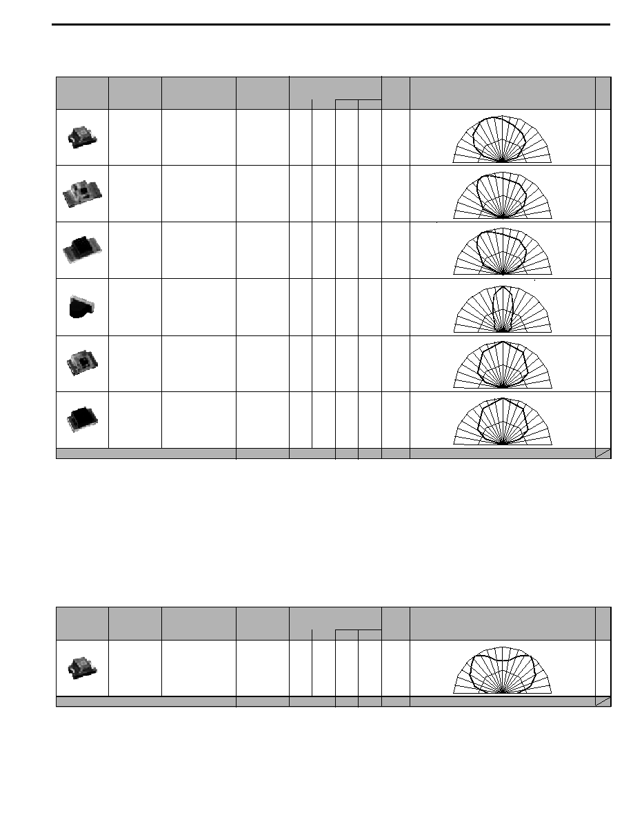
SMT SHAPE - PHOTO TRANSISTOR AND PIN PHOTO DIODE
n
Photo Transistor
Unit
nm
mA
V
m
s
mW/cm
2
Part No.
Features
Wavelength
of
Peak Sensitivity
l
P TYP.
V
CE
Spatial Distribution
(The typical distribution example of
each shape is shown below)
TYP.
TYP.
Shape
fig.
MIN.
Ee
Photo Current
I
C
Response
Time
tr ∑ tf
v
90
60
30
0
30
60
90
0.5
90
60
30
0
30
60
90
0.5
90
60
30
0
30
60
90
0.5
90
30
0
30
60
60
90
0.5
90
60
30
0
30
60
90
0.5
90
60
30
0
30
60
90
0.5
PS1101WA
PS1101RA
PS1191RA
PS1192FA
PS1102HA
PS1192HA
--
Reverse Mount
Reverse Mount
with visible radiation cut
filter under 700nm
Side view package
with visible radiation cut
filter under 700nm
Compact size
Compact size
with visible radiation cut
filter under 700nm
880
880
900
900
880
900
0.7
0.4
0.4
1.4
0.4
0.4
3.5
2.0
2.0
7.0
2.0
2.0
5
5
5
5
5
5
5
5
5
5
5
5
8/9
8/9
8/9
8/9
8/9
8/9
1
2
2
3
4
4
n
Pin Photo Diode
Unit
nm
mA
V
ns
mW/cm
2
Part No.
Features
Wavelength
of
Peak Sensitivity
l
P TYP.
V
CE
Spatial Distribution
(The typical distribution example of
each shape is shown below)
TYP.
Shape
fig.
MIN.
Ee
Photo Current
I
C
TYP.
Response
Time
tr ∑ tf
90
60
30
0
30
60
0.5
90
PP1101W
--
950
2.0
4.0
5
5
50
5
v
Ic=2mA, V
CE
=10V, R
L
=100
W
v
All above products contain no lead
Ta= 25∞C
Ta= 25∞C
v
Product contains no lead