N Channel MOSFET M01N60
1.0A
FEATURE
Robust High Voltage Temination.
Avalanche Energy Specified
Source-to Drain Diode Recovery Time
Comparable to a Discrete Fast Recovery Diode
Diode is Characterized for Use in Bridge
Circurits
I
DSS
and V
DS
(on) Specified at Elevated
Temperature
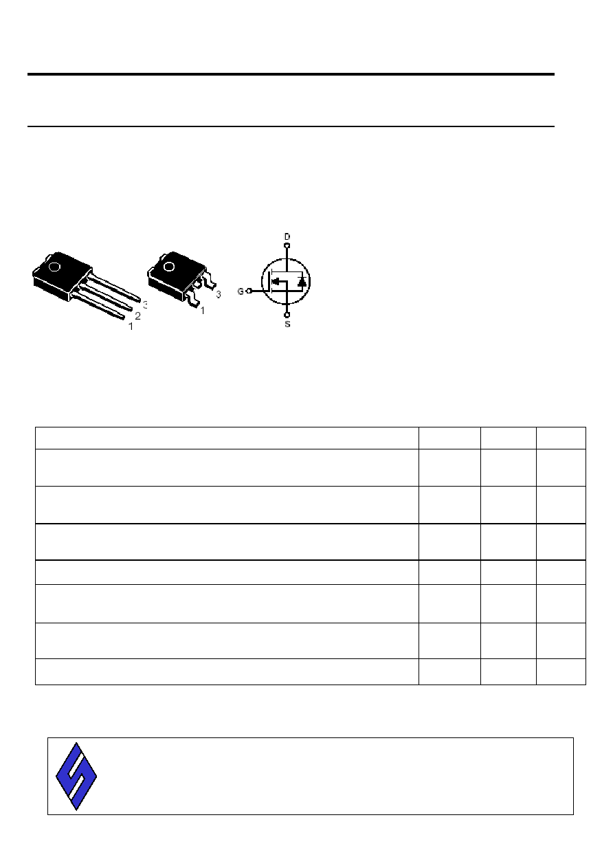
PIN CONFIGURATION
TO-251 TO-252
1.Gate 2.Drain 3.Source
ABSOLUTE MAXIMUM RATINGS
RATING SYMBOL
VALUE
UNIT
Drain to Current - Continuous
- Pulsed
I
D
I
DM
1.0
5.0
A
Gate-to-Source Voltage � Continue
- Non-repetitive
V
GS
V
GSM
+/-30
+/-40
V
V
Total Power Dissipation
TO-251/252
P
D
50
W
Operating and Storage Temperature Range
T
J
, T
STG
-55 to 150
Single Pulse Drain-to-Source Avalanche Energy � Tj = 25
(V
DD
=100V, V
GS
= 10V, I
AS
= 2A, L = 10mH, R
G
= 25)
E
AS
20
mJ
Thermal Resistance � Junction to Case
- Junction to Ambient
JC
JA
1.0
62.5
/W
Maximum Lead Temperature for Soldering Purposes, 1/8'' form 10 seconds
T
L
260
STANSON TECHNOLOGY
120 Bentley Square, Mountain View, Ca 94040 USA
TEL: (650) 9389294 FAX: (650) 9389295
Page 1

N Channel MOSFET M01N60
1.0A
MAXIMUM RATINGS AND ELECTRICAL CHARACTERISTICSTa=25
*Pulse Test: Pulse Width 300S, Duty Cycle 2%
**Negligible, Dominated by circuit inductance
PARAMETERS SYMBO
L
MIN
TYP MAX UNIT
CONDITION
Drain-Source Breakdown Voltage V
(BR)DSS
600
Vdc V
GS
=0, I
D
=250uA
Drain-Source Leakage Current
I
DSS
1.0
0.25
mA
mA
V
DS
=600V, V
GS
=0
V
DS
=480V, V
GS
=0, Tj=125
Gate-Source Leakage Current-
Forward
I
GSSF
100
nA V
GSR
=20V, V
DS
=0
Gate Threshhold Voltage
V
GS(th)
2.0 4.0
V V
DS
=V
GS
, I
D
=250uA
Drain-Source On-Resistance
R
DS(on)
8
Ohm
V
GS
=10V, I
D
=0.6A*
Input Capacitance
C
iss
210 pF
Output Capacitance
C
oss
28 pF
Reverse Transfer Capacitance
C
rss
9 pF
V
DS
=25V, V
GS
=0, f=1 MHz
Turn-On Delay Time
t
on
8 nS
Turn-Off Delay Time
t
off
18 nS
V
DS
=300V, I
D
=1.0A,
Rise Time
t
r
21 nS
Fall Time
t
f
24
nS
V
GS
=10V, R
G
=18
Total Gate Charge
Q
g
8.5 nC
Gate-Drain Charge
Q
gd
8.5
nC
V
DS
=400V, I
D
=1.0A
Gate-Drain Charge
Q
gs
1.8
nC V
GS
=10V*
Intemal Drain Inductance
L
D
4.5
nH
Measured from the drain lead
0.25'' From package to center
of die
Internal Drain Inductance
Ls
7.5
nH
Measured from the sorce lead
0.25'' package to source bond
pad
SOURCE-DRAIN DIODE CHARACTERISTICS
Forward On-Voltage(1)
VDS
1.5
V
Forward Tum Time
ton
**
nS
Reverse Recovery Time
trr
350
500
nS
Is=1.0A, VGS=0V
d
IS
/d
t
= 100A/
S
STANSON TECHNOLOGY
120 Bentley Square, Mountain View, Ca 94040 USA
TEL: (650) 9389294 FAX: (650) 9389295


