
Syntek Semiconductor Co., Ltd.
LCD Controller 1 / 1 ISSUE DATE: 3 March, 20000
STK55C643
STK55C643 Specification
1. FEATURES :
* Operating voltage : 2.5V - 4.0V.
* Maximum CPU operating frequency : 3.5MHz at 2.7V
* Dual oscillators :
- 32.768 KHz crystal oscillator for LCD display and watch timer.
- RC oscillator for system clock.
* 40 segments and 16 commons output for LCD driver.
- 1/5 bias, 1/16 duty and 64Hz frame frequency.
- 1/4 bias, 1/8 duty and 128Hz frame frequency.
* I/O port.
- 12 I/O pins.
- Port 1 with selectable interrupt.
* Built in 512 bytes RAM (including LCD storage area).
* Built in 48K bytes ROM for program.
* One 8-bit timer with 8 predefined input clock.
* Sound channel with voltage output type D/A.
* Five interrupt sources :
NMI - 64 Hz interrupt
IRQ1 - Stopwatch timer interrupt
IRQ2 - Fix-time timer interrupt
IRQ3 - Timer interrupt
IRQ4 - External interrupt
* Code option :
- Built-in 150K OHM pull-up resistors for I/O port.
- 1/8 duty or 1/16 duty.
2. APPLICATION :
* Calculator
* Hand-held game
* Small instrument
* Toy
Syntek Semiconductor Co., Ltd.
LCD Controller 2 / 2 ISSUE DATE: 3 March, 20000
STK55C643
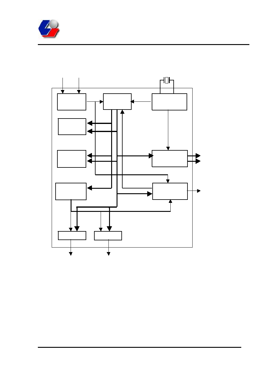
3. BLOCK DIAGRAM:
A0-A15
IRQ
D0-D7
P10-P17
P20-P23
8-bit CPU
Address
decoder
ROM
48Kx8
RAM
512x8
Clock
Generator
LCD driver
8-bit Timer
Port 1
Port 2
RC
oscillator
SOUND
32768Hz
C1-C16
S1-S40
OSC1
OSC2
Syntek Semiconductor Co., Ltd.
LCD Controller 3 / 3 ISSUE DATE: 3 March, 20000
STK55C643
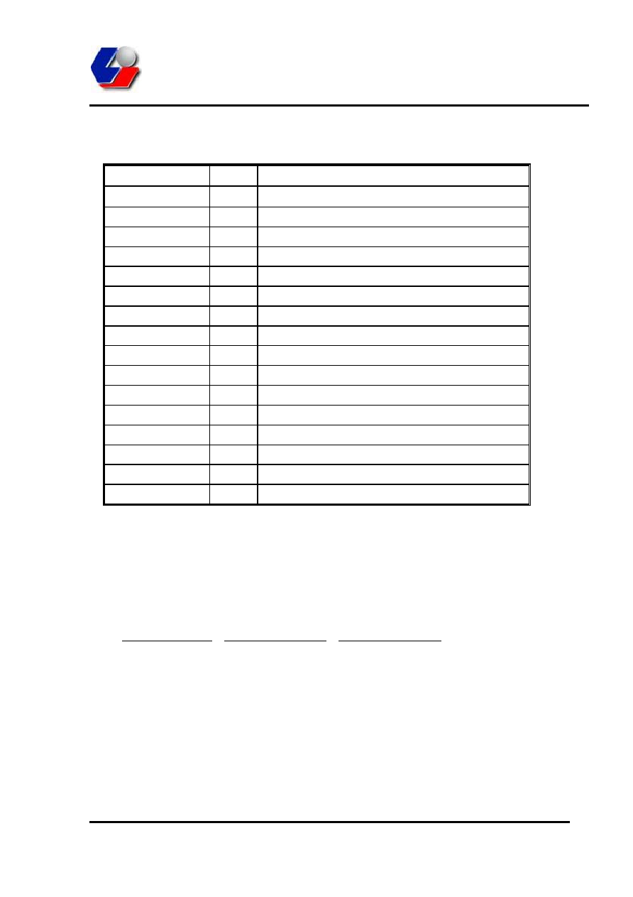
4. PIN DESCRIPTION :
(Total 80 pads)
Pin name
I/O
Function description
COM1-COM16
O
LCD common output pins
SEG1...SEG40
O
LCD segment output pins
VLCD
I
LCD voltage input
CLK256
O
256 Hz clock output
P10-P17
I/O
8-bit I/O pins for port 1
P20-P23
I/O
4-bit I/O pins for port 2
OSC1
I
Main system oscillator input pin for chip
OSC2
O
Main system oscillator output pin for resistor
XOSC1
I
32.768K Hz crystal oscillator input
XOSC2
O
32.768K Hz crystal oscillator output
SOUND
O
Sound output with volume control
/BUZ
O
Buzzer output
/RES
IU
System reset pin with internal 150K ohm pull-up.
/TEST
I
Test pin. Keep floating or connect to Vdd
VDD
Power input
VSS
Signal ground
5. ADDRESS ARRANGEMENT
1) RAM
0000-007F for LCD output data storage.
Memory address
Pin for 1/16 duty
Pin for 1/8 duty
0000-0004
COM1
COM1
0008-000C
COM2
COM2
0010-0014
COM3
COM3
0018-001C
COM4
COM4
0020-0024
COM5
COM5
0028-002C
COM6
COM6
0030-0034
COM7
COM7
0038-003C
COM8
COM16
0040-0044
COM9

Syntek Semiconductor Co., Ltd.
LCD Controller 4 / 4 ISSUE DATE: 3 March, 20000
STK55C643
Memory address
Pin for 1/16 duty
Pin for 1/8 duty
0048-004C
COM10
0050-0054
COM11
0058-005C
COM12
0060-0064
COM13
0068-006C
COM14
0070-0074
COM15
0078-007C
COM16
The LSB of low byte - SEG1.
The MSB of high byte - SEG40.
The middle bits are in the order.
0080-00FF : for zero page area.
0100-01FF : for stack and data area.
2) ROM
4000-FFFF for program area.
FFFF, FFFE - IRQ vector.
FFFD, FFFC - RES vector.
FFFB, FFFA - NMI vector.
3) Others
1000 To enter stand-by mode. Write only.
* Write this address, the CPU will be hold with LCD state no change.
* When in stand-by mode, the NMI and IRQ will wake up the CPU.
1001 To enter sleep mode. Write only.
= 1 Sleep mode 1
= 2 Sleep mode 2
All other values are prohibited. Do not write any other value to this register.
In sleep mode 1, both of the main system oscillator and 32.768KHz sub-system
oscillator will be stopped. So, all function are stopped and only external interrupt can
wake up this chip. The LCD display will be turn off while getting into sleep mode 1.
In sleep mode 2, only main system oscillator will be stopped. So, the following
functions will still keep working.

Syntek Semiconductor Co., Ltd.
LCD Controller 5 / 5 ISSUE DATE: 3 March, 20000
STK55C643
* The LCD will be kept on.
* The watch timer and fix-time timer will keep going.
* The NMI, port 1, watch timer and fix-time timer interrupt will wake up this chip.
* CPU will keep working if clock source is 32.768K Hz.
1002 Watch timer control register. Write only.
Bit 0 : = 0 Set watch timer interrupt at 10 Hz
= 1 Set watch timer interrupt at 100 Hz
1 : = 0 Set fix-time timer interrupt at 2 Hz
= 1 Set fix-time timer interrupt at 1 Hz
2 : = 0 Normal operation.
= 1 Reset and stop stopwatch timer.
3 : = 0 Stop stopwatch register without reset.
= 1 Start stopwatch timer.
4 : = 0 CPU clock is system clock.
= 1 CPU clock is 32.768K Hz.
7-5 : Reserved.
The default value for each bit is zero. Bit 2 will be cleared to zero automatically after
stopwatch timer reset.
1003 IRQ flag register. Read & write.
Read function :
Bit 0 : = 1 Stopwatch timer interrupt, IRQ1.
1 : = 1 Fix-time timer interrupt, IRQ2.
2 : = 1 Timer interrupt, IRQ3.
3 : = 1 External interrupt, IRQ4.
Write function :
Bit 0 : = 0 Clear stopwatch timer interrupt.
1 : = 0 Clear fix-time timer interrupt.
2 : = 0 Clear timer interrupt.
3 : = 0 Clear external interrupt.
Note : Please do not use the STZ $1003 to clear all the interrupts at the same time.
Also, please do not use the read-modify-write instruction to clear interrupt flag.
For example, LDA
#1 and TRB
$1003 to clear the IRQ1. Because some
other interrupts may be lost if clear interrupt with above method. Following
procedures are suggested.
LDA
$1003