 | –≠–ª–µ–∫—Ç—Ä–æ–Ω–Ω—ã–π –∫–æ–º–ø–æ–Ω–µ–Ω—Ç: STK85C161 | –°–∫–∞—á–∞—Ç—å:  PDF PDF  ZIP ZIP |

LCD Controller 1/20 Issue date : 22 September,1999
Syntek Semiconductor Co., Ltd.
STK85C161
Specification
1. FEATURES :
* Operating voltage : 2.5V ≠ 3.5 V.
* Maximum CPU operating frequency : 2MHz at 2.7V
* Oscillators :
- RC or 32.768 KHz crystal oscillator for LCD display and watch timer.
- Built-in PLL circuit to generate 4.19MHz system clock.
* 40 segments and 4 commons output for LCD driver.
- 1/3 bias, 1/4 duty and 64Hz frame frequency.
* 20 I/O pins.
-
8 I/O pins with selectable wake up interrupt.
-
4 general I/O pins.
-
8 I/O pin shared with S32-S39.
* Built in 160 bytes data RAM and 20 bytes write-only RAM for LCD display.
* Built in 96K bytes ROM with 16K bytes per bank for program.
* One 8-bit timer with 8 predefined input clock.
* Two sound generators and one voice channel with PWM outputs.
* Seven interrupt sources :
NMI - 64 Hz interrupt
IRQ1 - Fix-time timer interrupt
IRQ2 - Timer 1 interrupt
IRQ3 - External interrupt
IRQ4 - Timer 2 interrupt
IRQ5 - Sound generator 1 interrupt
IRQ6 - Sound generator 2 interrupt
* Code option :
-
Built-in 150K OHM pull-up resistors for I/O port.
-
RC or 32768Hz crystal oscillation for LCD driver.
2. APPLICATION :
* Talking Calculator
* Talking clock
* Hand-held game
LCD Controller 2/20 Issue date : 22 September,1999
Syntek Semiconductor Co., Ltd.
STK85C161
* Small instrument
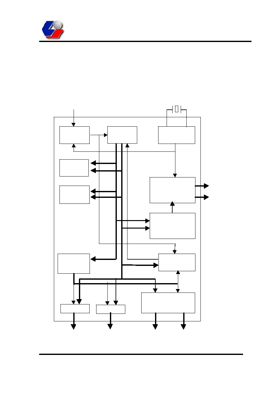
3. BLOCK DIAGRAM :
A0-A15
IRQ
D0-D7
P10-P17
P20-P23
PWM1
PWM2
8-bit CPU
Address
decoder
ROM
96Kx8
RAM
160x8
Clock
Generator
LCD driver
8-bit Timer
Port 1
Two sound generators
and one voice channel
with PWM output
PLL
32768Hz
C0-C3
S0-S39
VCAP
LCD RAM
20x8
Port 2
LCD Controller 3/20 Issue date : 22 September,1999
Syntek Semiconductor Co., Ltd.
STK85C161
4. PIN DESCRIPTION :
(Total 72 pads)
Pin name
I/O
Function description
COM0-COM3
O
LCD common output pins
SEG0-SEG39
O
LCD segment output pins
P10-P17
I/O
8-bit I/O pins for port 1
P20-P23
I/O
4-bit I/O pins for port 2. P23 can be set as output with
carrier clock.
P30-P37
I/O
8-bit I/O pins for port 3. These pins are shared with
S32-S39.
VCAP
I/O
Low pass filter capacitor for PLL.
XOSC1
I
32.768K Hz crystal oscillator input
XOSC2
O
32.768K Hz crystal oscillator output
PWM1
PWM2
O
Sound channel PWM output with volume control.
/RES
I
System reset pin with 100K pull-up resistor.
VLCD
I
Bias voltage input pin.
VC2
I
2/3Vlcd bias voltage input pin.
VC1
I
1/3Vlcd bias voltage input pin.
C1A, C1B
Booster capacitor connection pins
C2A, C2B
Booster capacitor connection pins
/TEST
I
Test pin. Keep floating or connect to Vdd
VDD1
Power input for PWM output
VSS1
Signal ground for PWM output
VDD
Power input
VSS
Signal ground
LCD Controller 4/20 Issue date : 22 September,1999
Syntek Semiconductor Co., Ltd.
STK85C161
5. ADDRESS ARRANGEMENT
1)
LCD Data latches
0000-001C for LCD output data storage. The memory addresses, which are not specified in
the table, are not implemented. This area is write only.
SEG0-SEG7 SEG8-SEG15
∑
∑
∑
SEG31-SEG39
COM0
0000
0001
∑
∑
∑
0004
COM1
0008
0009
∑
∑
∑
000C
COM2
0010
0011
∑
∑
∑
0014
COM3
0018
0019
∑
∑
∑
001C
The LSB of low byte ≠ SEG0.
The MSB of high byte ≠ SEG39.
The middle bits are in the order.
2) RAM
0040-00DF for zero page area.
0140-01DF for stacks. This area is overlapped with 0040-00DF.
3) ROM
8000-BFFF For program bank area.
C000-FFFF for program area. This area is always mapping to the last 16K bytes of internal
ROM and it is not affected by the bank setting.
FFFF, FFFE - IRQ vector.
FFFD, FFFC - RES vector.
FFFB, FFFA - NMI vector.
4) Others
1000 To enter stand-by mode. Write only.
* Write this address, the CPU will be hold with LCD state no change.
* When in stand-by mode, the NMI and IRQ will wake up the CPU.
1001 To enter sleep mode. Write only.
Bit 0 = 1 Sleep mode 1

LCD Controller 5/20 Issue date : 22 September,1999
Syntek Semiconductor Co., Ltd.
STK85C161
1 = 1 Sleep mode 2
In sleep mode 1, both of the main system oscillator and 32.768KHz sub-system
oscillator will be stopped. So, all functions are stopped and only external interrupt can
wake up this chip. The LCD display will be turn off while getting into sleep mode 1. If
the LCD is turned on after wake-up immediately, then some garbage may display on the
LCD. It is better to turn off the LCD by software before enter sleep mode 1. After wake
up, the software has to delay several ms before turn on the LCD because the crystal will
take several mS to stable.
In sleep mode 2, only main system oscillator will be stopped. So, the following functions
will still keep working.
* The LCD will be kept on.
* The fix-time timer will keep going.
* The NMI, port 1, and fix-time timer interrupt will wake up this chip.
* CPU will keep working if clock source is 32.768K Hz.
1002 Watch timer control register. Write only.
Bit 1 : = 0 Set fix-time timer interrupt at 2 Hz
= 1 Set fix-time timer interrupt at 1 Hz
7-2 : Reserved.
The default values for each bit is zero.
1003 IRQ flag register. Read & write.
Read function :
Bit 0 : = 1 Fix-time timer interrupt, IRQ1.
1 : = 1 Timer 1 interrupt, IRQ2.
2 : = 1 Port 1 interrupt, IRQ3.
3 : = 1 Timer 2 interrupt, IRQ4.
4 : = 1 Sound generator 1 (timer3) interrupt, IRQ5.
5 : = 1 Sound generator 2 (timer4) interrupt, IRQ6.
Write function :
Bit 0 : = 0 Clear fix-time timer interrupt.
1 : = 0 Clear timer 1 interrupt.
2 : = 0 Clear port 1 interrupt.
3 : = 0 Clear timer 2 interrupt.
4 : = 0 Clear sound generator 1 (timer3) interrupt.