 | –≠–ª–µ–∫—Ç—Ä–æ–Ω–Ω—ã–π –∫–æ–º–ø–æ–Ω–µ–Ω—Ç: 1HNK60R | –°–∫–∞—á–∞—Ç—å:  PDF PDF  ZIP ZIP |

1/15
November 2004
STD1NK60 - STD1NK60-1
STQ1HNK60R - STN1HNK60
N-CHANNEL 600V - 8
- 1A DPAK/TO-92/IPAK/SOT-223
SuperMESHTM MOSFET
Table 1: General Features
s
TYPICAL R
DS
(on) = 8
s
EXTREMELY HIGH dv/dt CAPABILITY
s
ESD IMPROVED CAPABILITY
s
100% AVALANCHE TESTED
s
NEW HIGH VOLTAGE BENCHMARK
s
GATE CHARGE MINIMIZED
DESCRIPTION
The SuperMESHTM series is obtained through an
extreme optimization of ST's well established
strip-based PowerMESHTM layout. In addition to
pushing on-resistance significantly down, special
care is taken to ensure a very good dv/dt capability
for the most demanding applications. Such series
complements ST full range of high voltage MOS-
FETs including revolutionary MDmeshTM products.
APPLICATIONS
s
LOW POWER BATTERY CHARGERS
s
SWITH MODE LOW POWER
SUPPLIES(SMPS)
s
LOW POWER, BALLAST, CFL (COMPACT
FLUORESCENT LAMPS)
Table 2: Order Codes
Figure 1: Package
Figure 2: Internal Schematic Diagram
TYPE
V
DSS
R
DS(on)
I
D
Pw
STD1NK60
STD1NK60-1
STQ1HNK60R
STN1HNK60
600 V
600 V
600 V
600 V
< 8.5
< 8.5
< 8.5
< 8.5
1 A
1 A
0.4 A
0.4 A
30 W
30 W
3 W
3.3 W
3
2
1
TO-92 (Ammopack)
IPAK
1
2
2
3
SOT-223
1
3
DPAK
Part Number
Marking
Package
Packaging
STD1NK60T4
D1NK60
DPAK
TAPE & REEL
STD1NK60-1
D1NK60
IPAK
TUBE
STQ1HNK60R
1HNK60R
TO-92
BULK
STQ1HNK60R-AP
1HNK60R
TO-92
AMMOPAK
STN1HNK60
1HNK60
SOT-223
TAPE & REEL
Rev. 2

STD1NK60 - STD1NK60-1 - STQ1HNK60R - STN1HNK60
2/15
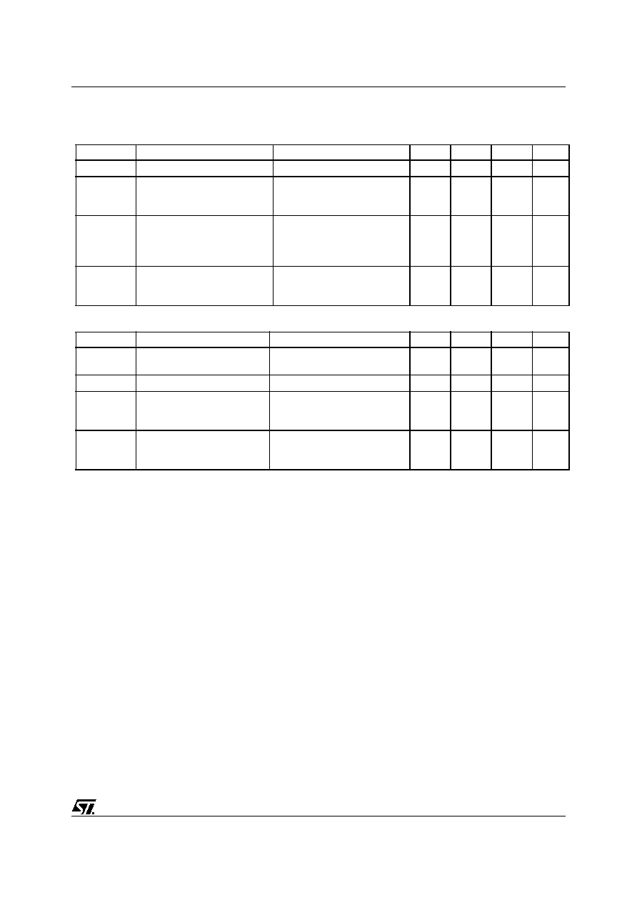
Table 3: Absolute Maximum ratings
( ) Pulse width limited by safe operating area
(1) I
SD
1.0A, di/dt
100A/µs, V
DD
V
(BR)DSS
, T
j
T
JMAX.
Table 4: Thermal Data
(#) When mounted on FR-4 board of 1 in
2
, 2oz Cu, t < 10 sec
Table 5: Avalanche Characteristics
ELECTRICAL CHARACTERISTICS (T
CASE
=25∞C UNLESS OTHERWISE SPECIFIED)
Table 6: On/Off
Symbol
Parameter
Value
Unit
DPAK / IPAK
TO-92
SOT-223
V
DS
Drain-source Voltage (V
GS
= 0)
600
V
V
DGR
Drain-gate Voltage (R
GS
= 20 k
)
600
V
V
GS
Gate- source Voltage
± 30
V
I
D
Drain Current (continuous) at T
C
= 25∞C
1.0
0.4
0.4
A
I
D
Drain Current (continuous) at T
C
= 100∞C
0.63
0.25
0.25
A
I
DM
( )
Drain Current (pulsed)
4
1.6
1.6
A
P
TOT
Total Dissipation at T
C
= 25∞C
30
3
3.3
W
Derating Factor
0.24
0.025
0.025
W/∞C
dv/dt (1)
Peak Diode Recovery voltage slope
3
V/ns
T
j
T
stg
Operating Junction Temperature
Storage Temperature
-55 to 150
∞C
DPAK/IPAK
TO-92
SOT-223
Unit
Rthj-case
Thermal Resistance Junction-case Max
4.16
--
--
∞C/W
Rthj-amb
Thermal Resistance Junction-ambient Max
100
120
37.87 (#)
∞C/W
Rthj-lead
Thermal Resistance Junction-lead Max
--
40
--
∞C/W
T
l
Maximum Lead Temperature For Soldering
Purpose
275
260
∞C
Symbol
Parameter
Max Value
Unit
I
AR
Avalanche Current, Repetitive or Not-Repetitive
(pulse width limited by T
j
max)
1
A
E
AS
Single Pulse Avalanche Energy
(starting T
j
= 25 ∞C, I
D
= I
AR
, V
DD
= 50 V)
25
mJ
Symbol
Parameter
Test Conditions
Min.
Typ.
Max.
Unit
V
(BR)DSS
Drain-source
Breakdown Voltage
I
D
= 1mA, V
GS
= 0
600
V
I
DSS
Zero Gate Voltage
Drain Current (V
GS
= 0)
V
DS
= Max Rating
V
DS
= Max Rating, T
C
= 125 ∞C
1
50
µA
µA
I
GSS
Gate-body Leakage
Current (V
DS
= 0)
V
GS
= ± 30V
±100
nA
V
GS(th)
Gate Threshold Voltage
V
DS
= V
GS
, I
D
= 250 µA
2.25
3
3.7
V
R
DS(on)
Static Drain-source On
Resistance
V
GS
= 10V, I
D
= 0.5 A
8
8.5
3/15
STD1NK60 - STD1NK60-1 - STQ1HNK60R - STN1HNK60
ELECTRICAL CHARACTERISTICS (CONTINUED)
Table 7: Dynamic
Table 8: Source Drain Diode
(1) Pulsed: Pulse duration = 300 µs, duty cycle 1.5 %.
(2) Pulse width limited by safe operating area.
Symbol
Parameter
Test Conditions
Min.
Typ.
Max.
Unit
g
fs
(1)
Forward Transconductance
V
DS
= 15 V
,
I
D
= 0.5 A
1
S
C
iss
C
oss
C
rss
Input Capacitance
Output Capacitance
Reverse Transfer Capacitance
V
DS
= 25V, f = 1 MHz, V
GS
= 0
156
23.5
3.8
pF
pF
pF
t
d(on)
t
r
t
d(off)
t
r
Turn-on Delay Time
Rise Time
Turn-off Delay Time
Fall Time
V
DD
= 300 V, I
D
= 0.5 A,
R
G
= 4.7
,
V
GS
= 10 V
(Resistive Load see, Figure
21)
6.5
5
19
25
ns
ns
ns
ns
Q
g
Q
gs
Q
gd
Total Gate Charge
Gate-Source Charge
Gate-Drain Charge
V
DD
= 480V, I
D
= 1 A,
V
GS
= 10V, R
G
= 4.7
(see, Figure 23)
7
1.1
3.7
10
nC
nC
nC
Symbol
Parameter
Test Conditions
Min.
Typ.
Max.
Unit
I
SD
I
SDM
(2)
Source-drain Current
Source-drain Current (pulsed)
1
4
A
A
V
SD
(1)
Forward On Voltage
I
SD
= 1.0 A, V
GS
= 0
1.6
V
t
rr
Q
rr
I
RRM
Reverse Recovery Time
Reverse Recovery Charge
Reverse Recovery Current
I
SD
= 1.0 A, di/dt = 100 A/µs
V
DD
= 25V, T
j
= 25∞C
(see test circuit, Figure 22)
140
240
3.3
ns
µC
A
t
rr
Q
rr
I
RRM
Reverse Recovery Time
Reverse Recovery Charge
Reverse Recovery Current
I
SD
= 1.0 A, di/dt = 100 A/µs
V
DD
= 25V, T
j
= 150∞C
(see test circuit, Figure 22)
229
377
3.3
ns
µC
A

STD1NK60 - STD1NK60-1 - STQ1HNK60R - STN1HNK60
4/15
Figure 3:
.
Safe Operating Area For SOT-223
Figure 4: Safe Operating Area For DPAK/IPAK
Figure 5: Safe Operating Area For TO-92
Figure 6: Thermal Impedance For SOT-223
Figure 7: Thermal Impedance For DPAK/IPAK
Figure 8: Thermal Impedance For TO-92

5/15
STD1NK60 - STD1NK60-1 - STQ1HNK60R - STN1HNK60
Figure 9: Output Characteristics
Figure 10: Transconductance
Figure 11: Capacitance Variations
Figure 12: Transfer Characteristics
Figure 13: Gate Charge vs Gate-source Voltage
Figure 14: Static Drain-source On Resistance